
Thangavel Vinotha* | Bhavani Gnanasambandam Geetha
© 2026 The authors. This article is published by IIETA and is licensed under the CC BY 4.0 license (http://creativecommons.org/licenses/by/4.0/).
OPEN ACCESS
Wafer production comprises an intricate procedure, where the examination of the wafers is a crucial component. During the quality control process, the team utilizes a wafer prober to measure the electrical performance of the individual die sites. Depending on this assessment, the useful or defective dies are classified and identified through a color-coding system on a wafer map. Examining the wafer map is advantageous for quality assurance and evaluating the manufacturing process within the semiconductor industry. A wafer map shows information regarding several flaw layouts on the substrate material surface. By precisely detecting diverse defect patterns shown on the wafer map, engineers can identify production line issues, simplify the integrated circuit fabrication process, and minimize the number of rejected items. An iterative refinement of the manufacturing process has substituted manual wafer defect pattern recognition with an automated analysis through embedded devices, drastically improving efficiency. With the advent of large-scale data sets, researchers started using established artificial intelligence and neural network methods to classify semiconductor wafer defect configurations. This study presents a fine-grained deep convolutional neural network-based wafer map defect detection and classification (FGDCNN-WMDDC) technique for semiconductor manufacturing. The objective of the proposed model is to detect and classify different types of manufacturing defects in silicon wafers, such as center, donut, edge local, edge ring, local, near full, none, random, and scratch. The proposed model follows an end-to-end architecture comprising pre-processing, feature extraction, and classification. Initially, the proposed model applies adaptive bilateral filtering and a contrast enhancement process as a pre-processing step. Next, the Dual Attention EfficientNet model is applied, which can actively learn and automatically extract effective classification features. To improve the performance of the DL approach, the hyperparameter selections are performed using the use of Nadam optimizer. Finally, a stacked sparse autoencoder (SSAE) is applied for the detection and classification of distinct defect types. The performance validation of the proposed model is tested using WM811k Silicon Wafer Map Dataset Image dataset. Extensive experimental results highlighted that the proposed model performs well over other models in terms of different measures. Therefore, the proposed model can be applied as a robust tool for automated detection of distinct defects that exist in wafer map.
wafer map defect, semiconductor manufacturing, computer vision, EfficientNet, hyperparameter selection
Currently, the semiconductor industry is developing quickly, and as a result of considerable technological developments, more classified products are being designed and produced [1]. Semiconductor devices are occupying almost every aspect of the modern world, from smartphones to ultra-high specification television sets [2]. To sustain the ever-increasing demand for low-priced, higher memory capacity devices, and/or faster computing power, the design of the semiconductor production process is developing into a more difficult process that needs the introduction of complex assemblies, new manufacturing methods, new hardware components, and strict monitoring of cleaning and managing the systems [3]. The introduction of innovative aspects of the production procedure could be a main source of unwanted particles of material deposition. Also, modifications in present process conditions can result in particle generation based on the reaction dynamics of the model [4]. These particle faults on semiconductor wafers could be one of the major reasons for product failure. To understand the effect of production tools on their faults, the standard practice in the semiconductor material industry is to process thousands of wafers per annum per classification tool, like optical scattering and scanning electron microscopy tools [5]. Every wafer can consist of tens of faults. As the production process and, therefore, particle defect configurations become more difficult, the quantity of defects considerably increases.
Wafer production involves many intricate phases and variables. In the modern era, the growing difficulty and density of wafer designs have caused an increase in defect variety inside semiconductor wafers [6]. The classification of these defects provides a particular difficulty in relating to the unique defects because of their variations in orientation and location in the wafer [7]. Therefore, the effective categorizations of such defects signify a crucial analysis endeavor in semiconductor production procedures. The Wafer map classification and Manual feature extraction pose a significant problem relating to lab and time for engineers [8]. Recently, Artificial Intelligence (AI), especially machine learning (ML) methods, has established its efficiency in exactly identifying defects by extracting different features, surface textures, and critical pattern data. Particularly, deep learning (DL) models for semiconductor defect detection have been made a considerable process [9]. Researchers discovered that the utilization of convolutional neural networks (CNNs) has led to recent advancements in the state-of-the-art image classification operation, and developed a traditional method for addressing any image classification challenges. CNN is the end-to-end technique and does not need any task-specific feature engineering [10]. This end-to-end technique is useful as we don’t need to improve the task-specific feature extractors, and the field-specific expert knowledge is unnecessary. Another point of image classification is the difficulty of image recovery [11]. The image recovery is a challenge of finding images comprising the same scene or objects, providing query images, and it was employed in security and monitoring, medical images, and several fields [12]. Usually, the image recovery needs feature extraction employing object shape and colours. As the deep CNN can learn strong features at every layer, such standard features are utilized as good descriptions for image recovery [13]. CNN has presented an excellent operation compared to other classification methods, provoking a comprehensive study in the domain of wafer map pattern categorization.
To precisely identify wafer map defects in semiconductor manufacturing, this paper focuses on the design and development of a novel fine-grained deep convolutional neural network-based wafer map defect detection and classification (FGDCNN-WMDDC) approach. The proposed model intends to classify nine different types of wafer map defects using advanced models. This study follows a multi-faceted approach integrating preprocessing, feature representation, parameter tuning, and classification. The proposed model is evaluated on the benchmark datasets under several measures. The following are the major contributions of this research:
•Integrate Dual Attention EfficientNet architecture for robust feature extraction, which proficiently captures highly discriminative features contributing to the classification process.
•Utilize Nadam optimizer for hyperparameter optimization, which helps attain improved model convergence and better model performance with less computational complexity.
•Employ stacked sparse autoencoder (SSAE), a DL-based model for wafer defect detection and classification, are utilized and effectively classifies nine different classes.
•Conduct extensive experiments and demonstrate improved performance of the model compared to other baseline models across diverse measures.
This section provides a concise assessment of recent and relevant studies focusing on wafer map defect detection and classification techniques. Lee et al. [14] presented a CNN integrated with a data transformation technique at the feature extraction phase, combining Radon-based features and Density-driven features to develop the representation of key patterns. Consequently, several classifiers are combined employing bagging, voting, and AdaBoost methods to enhance the classification process and generalization of the system. The method is intended to mitigate data inequity and choice bias by using random sampling and assigning different weights to each classifier. Furthermore, this method is an ensemble learning architecture combining several classifiers with optimized weighting mechanisms to improve classification strength. Taha [15] presented a method using ML classification models to identify wafer defects in semiconductor production. In spite of the increasing body of studies representing the efficiency of ML in wafer defect recognition, there is a conspicuous lack of complete evaluations on this issue. Altantawy and Yakout [16] presented an innovative hybrid deep method for wafer map defect identification to address these difficulties. Initially, an innovative convolutional auto-encoder (CAE) is used as a synthesis technique to adjust the huge imbalance issue of the dataset. Next, for effective dimension reduction, an embedding process is implemented in the synthesised maps to gain sparse encrypted wafer maps by supporting a sparsity regularisation in an encoder and decoder system to compose a sparsity-boosted AE (SBAE).
Tsai and Wang [17] presented a global-to-local generative adversarial network (G2LGAN) technique employing the DL architecture. The author employs random under-sampling to overpower the popular data. The author utilizes MobilenetV2 as the classifier and employs 2 datasets for validation. This method integrates data improvement and random under-sampling techniques to enhance the database and employ this classification network for categorization tasks. Souri et al. [18] presented an enhanced hybrid DL architecture, which incorporated CNN for extracting spatial features with Long Short-Term Memory (LSTM) systems to model temporal dependences in defect patterns. By integrating spatial and sequential data, this system improves the accuracy of defect classification related to conventional techniques. Its robustness lies in the combined spatial–temporal learning that captures difficult defect characteristics more efficiently. Kim and Kim [19] presented a model for improving the feature extraction operation of defect patterns by changing the spherical coordinate model before the present WBM images. In order to decrease the inconsistency of the position, defect patterns in the Cartesian coordinate model, but the location of the disseminated defect die is not persistent, were transformed to a spherical coordinate system. Lastly, this method is an automated pattern categorization model that employs each classifier to discover the defect categories, followed by implementing collaborative models for several defect pattern classifications.
Xie et al. [20] presented an innovative Hypergraph Convolutional Network for the automatic Wafer Defect Identification (HCN-WDI). The HCN is applied as an end-wise operator to detect WDI, and 3 standard image classifiers are employed as feature extractions and baselines for this HCN-WDI system. Deng and Wang [21] presented a light-weight NN technique to effectively detect mixed-type wafer defects. Great kernel convolutions assist the model in retaining the significant features while down-sampling processes. Related to a few popular higher-performance techniques and light-weight systems, this method has benefits in both detection accuracy and processing speed.
Current wafer map defect detection techniques can be broadly classified into ensemble learning techniques (E), lightweight neural architectures (L), generative adversarial techniques (G), and autoencoder based DL (A). Ensemble learning techniques are more robust in classification, but are generally more complex in computation and less scalable. Lightweight architectures are low in computational complexity, but can have disadvantages in the fine-grained feature extraction capability in complex wafer defect scenarios. Data imbalance is effectively solved by GAN and autoencoder based methods, but these methods are limited in spatial attention modeling and feature representation. Moreover, some current approaches have drawbacks, such as their inability to deal with visually similar categories of defects and their poor classification accuracy when the number of samples in each category varies widely. To address these challenges, the proposed FGDCNN-WMDDC framework combines Dual Attention EfficientNet feature learning with Nadam optimization and SSAE classification to achieve better discriminative learning and perform wafer defect classification better.
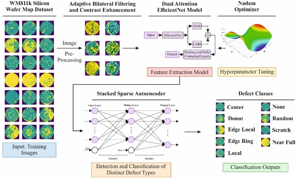
This section defines the architecture and working principles of the proposed FGDCNN-WMDDC system for accurate wafer map defect detection and classification. Figure 1 depicts the overall structural design of the FGDCNN-WMDDC model. As depicted in Figure 1, images were first attained from WM811k Silicon Wafer Map Dataset Image dataset and then applied an adaptive bilateral filter (ABF) and contrast enhancement models to prepare the images for effective analysis by improving their quality. Following preprocessing, feature extraction takes place through a Dual Attention EfficientNet architecture. This model captures crucial features that influence the defect patterns. Then, the proposed model integrates the Nadam optimizer to fine-tune the model parameters for better performance. The selected feature sets are then input to the SSAE, which performs accurate defect type classification.
Figure 1. Overall structural design of the fine-grained deep convolutional neural network-based wafer map defect detection and classification (FGDCNN-WMDDC) model
3.1 Image preprocessing module
This subsection describes the preprocessing techniques used to improve the quality of wafer map images before feature extraction. In this study, an ABF and CLAHE are employed.
ABF: This method is broadly employed in image processing and CV for the edge-preserving smoothing process [22]. Unlike linear convolution filters, the BF employs a variety of kernels as well as a spatial kernel; these are commonly Gaussian. This module, which evades pixel blending with larger intensity changes, assures the protection of sharp edges, making the filter both non-linear and computationally in-depth. In ABF, the measure of the width and center of the range kernel of the Gaussian are permitted for modifying pixelwise.
Here, $f: \mathbb{I} \rightarrow \mathbb{R}$ denotes input imaging, $\mathbb{I} \subset \mathbb{Z}^2$ signifies the omain of image. $g: \mathbb{I} \rightarrow \mathbb{R}$ implies the output image.
$g(i)=\eta(i)^{-1} \sum_{j=\Omega} \omega(j) \phi(f(i-j)-\theta(i)) f(i-j)$ (1)
$\eta(i)=\sum_{j \in \Omega} \omega(j) \phi_i(f(i-j)-\theta(i))$ (2)
where, $\Omega$ signifies window centered with the origin, and $\phi_i: \mathbb{R} \rightarrow \mathbb{R}$ denotes local Gaussian range kernel:
$\phi_i(t)=\exp \left(-\frac{t^2}{2 \sigma(i)^2}\right)$ (3)
Notably, the center $\theta(i)$ in Eq. (1) and width $\sigma(i)$ in Eq. (3) were structurally differing operations. The spatial kernel $\omega: \Omega \rightarrow \mathbb{R}$ in Eq. (1) was a Gaussian equation as given by,
$\omega(j)=\exp \left(-\frac{\|j\|^2}{2 \rho^2}\right)$ (4)
CLAHE: CLAHE is employed to enhance contrast in wafer map imagery while boosting image quality and improving the performance of classification and detection for various defect forms. Initially, the wafer map imaging is separated into minor parts by nominal separation, and then equalization of the histogram is used for every separation. To equalize the value of gray in the images, hidden features of the image shape are more noticeable. The sharp corners of the imaging are prevented by limitations in the grey spectrum and area.
Where CLAHE is employed for limiting the amplification that is measured utilizing a clipping histogram at some level. The Rayleigh distribution is applied for clipping the histogram that is mathematically computed in Eq. (5).
$g=g_{\min }\left[2\left(\beta^2\right) \ln +\left(\frac{1}{1-p(F)}\right)\right]^{0.5}$ (5)
Here, $g$ and $g_{\min}$ denotes the determined and minimal value of pixel, $\beta$ denotes the threshold parameter, and $p(F)$ implies a distribution function. These improve wafer imaging support to the next stage of feature extraction.
3.2 Feature learning
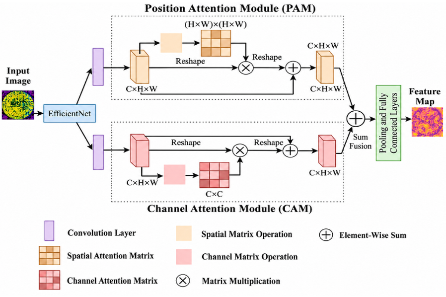
This subsection specifies the extraction of meaningful attributes from wafer map images to assist in precise defect classification. In this paper, a Dual Attention EfficientNet model is utilized to extract both spatial and channel-wise relationships in wafer map defect patterns by a two-attention mechanism, which results in classifying changes among the wafer map defect classes. The primary goal of the attention mechanism is to choose a significant region of input information that doesn’t consider the areas with weak and non-discriminative defect attributes. These mechanisms concentrate on differentiating the feature extraction from several areas of wafer map imaging. In this study, the Dual Attention module is used to eliminate the interference of irrelevant data and focus more on the valuable defect-related data. Position Attention Mechanism (PAM) and Channel Attention Mechanism (CAM) have been integrated with EfficientNet-B0 to regulate the relations among the global and local features.
PAM: To extract the contextual information from lower‐level features, PAM is used for learning more information to enhance the feature representation. The PAM architecture is intended to gather and detect relevant features associated with the spatial domain. The major benefit of PAM is learning the spatial interdependency of features and gaining several contextual data points from local components. The input feature mapping $A$ is computed as in Eq. (6).
$A=F \in R^{C \times H \times W}$ (6)
Let, $F$ implies features; $C$ signifies the number of relevant features in the spatial domain, $H$ indicates the height of the spatial dimension; $W$ implies the spatial dimension width of the input tensor. The PAM makes a positional relations method between features for acquiring global feature data and integrates features randomly by the total weights allocated for features at every position. The input feature mapping performs a convolution function with a BN layer and a Rectified Linear Unit (ReLU) layer for providing the three novel feature maps F1, F2, and F3. These maps are known as single‐channel feature maps that are attained from F, the feature maps F1 and F2 are of similar dimensions, but F3 has various dimensions. After the performance of the reshape function on F1, F2, and F3, the scaling of feature maps becomes $H \times W$ then perform a matrix multiplication. Therefore, the last output $F \in R^{C \times H \times W}$ is developed over the multiplication of differentiated outcomes achieved by learnable parameters $\delta$ and an element-wise addition with the original feature mapping is expressed in Eq. (7).
$F^{\prime \prime}=\delta \cdot {reshape}\left(V \cdot M_p\right)+F^{\prime}$ (7)
CAM: Channel attention is used to update features of various channels to simulate the significance of each channel from the feature extraction. The CAM detects relationships in the local cross‐channel to evaluate the channel and its neighbours. Therefore, the number of parameters is lessened, and the model difficulty is also decreased without compromising the precision. In CAM, transition and dense block layers are combined to avoid adding many parameters that result in overfitting. The transition layer in CAM contains $1 \times 1$ a convolutional (Conv) layer as well as an average pooling layer with a stride of two for reducing the feature map size. This mechanism is divided into two stages, like the squeeze and excitation.
In squeeze stages, input attributes are compressed into one‐dimensional vector lengths that signify the number of channels. In the excitation phase, dependencies between the channels are gathered by a gate mechanism, which comprises dual non-linear fully connected (FC) layers. To squeeze and expand feature channels, CAM allocates adaptive weights to several features. The mathematical expression of the output of CAM is signified in Eq. (8).
$\beta(U)=\sigma\left(W_1 W_2\left(U_{a v g}+U_{\max }\right)\right)$ (8)
Here, $\sigma$ denotes the activation function of the sigmoid $W_1$ and $W_2$ implies the weights of the FC layer, $U_{a v g}$ and $U_{\max }$ denotes the average and maximal pooling feature map.
EfficientNet-B0: EfficientNet-B0 is a CNN technique that uses a complex scale approach for image recognition and identification. The network is scaling along with optimizing the width, depth, and resolution, which leads to enhancing the network. The primary goal of EfficientNet-B0 structure is to find an appropriate model for scaling the CNN technique to attain high precision for the recognition, classification, or detection process. Therefore, the scaled width of the network layers is obtained, resulting in more fine-tuned features and training the model. Nevertheless, wide and shallow layers in the network are not capable of learning from higher-level features, and high‐resolution imaging is employed for learning fine-grained and complex patterns. Later, regulating these depths, width, and resolution, EfficientNet-B0 enhances the classification execution.
Numerous Conv layers with 3 × 3 receptive fields and mobile inverted bottleneck Conv layers effectively attain information from the features extracted for wafer map defect classification. The scaling depth, width, and resolution in EfficientNet-B0 are shown in Eqs. (9)-(13).
$d=\alpha \varphi$ (9)
$w=\beta \varphi$ (10)
$r=\gamma \varphi$ (11)
$\operatorname{s.t} \alpha \cdot \beta 2 . \gamma 2 \approx 2$ (12)
$\alpha \geq 1, \quad \beta \geq 1, \quad \gamma \geq 1$ (13)
Here, $r$, $w$, and $d$ denote the network’s resolutions, width, and depth; constant terms $\alpha, \beta$, and $\gamma$ are attained employing the grid search parameter-graining approach. A coefficient is a user-defined variable that allocates scaled resources for each technique in the network. By fine-graining the resolution, width, and depth of the network, optimize the network precision and memory consumption consistent with the accessible sources. Unlike deep CNNs, a predefined set of scaling coefficients is employed in EfficientNet-B0 to regulate every dimension of layers in the network, which outperforms the prior cutting-edge techniques trained on ImageNet database. An incorporation of Dual Attention in Efficient-B0 improves the learning of the most important data about defect levels of the wafer map from pre-processed images. Figure 2 represents the model diagram of Dual Attention EfficientNet.
Figure 2. Model diagram of Dual Attention EfficientNet
3.3 Model optimization
This subsection presents the optimization strategy exploited to improve model performance. Nadam is an optimizer algorithm that integrates the adaptive learning rate mechanism of Adam with the lookahead gradient method of Nesterov accelerated gradient (NAG). Although the conventional momentum approach adjusts parameter upgrades that depend on collected gradients from prior phases, Nesterov momentum expects future gradient directions, allowing more informed upgrades. Nadam combines this foresight into Adam’s adaptive upgrade structure, enabling parameters for converging more effectively toward optimal solutions. This incorporation results in quicker convergence and enhanced stability in training, particularly in non-convex optimizer issues or when handling the noisy gradients. Therefore, Nadam is broadly accepted as an improved optimization in NN training, and it played an important part in enhancing training efficacy and overall model execution. The weights are upgraded based on:
$w_t^i=w_{t-1}^i-\frac{\eta}{\sqrt{v_t+e}} \cdot \widetilde{m}_t$ (14)
$\tilde{m}_t=\beta_1^{t+1} \widehat{m}_t+\left(1-\beta_1^t\right) \hat{g}_t$ (15)
$\hat{m}_t=\frac{m_t}{1-\Pi_{i=1}^t \beta_1^i}$ (16)
$\hat{g}_t=\frac{g_t}{1-\Pi_{i=1}^t \beta_1^i}$ (17)
Here, $\eta$ denote the learning rate of the parameter, and $w_t$ implies weights at step $t$. Even though, $\beta_i$ signifies applied to choose the number of data required from the last upgrade, here $\beta_i \in[0,1], m_t$ denote the initial moment.
Table 1 summarizes the optimal hyperparameter configuration adopted to ensure stable and efficient model training. The EfficientNet backbone integrated with PAM/CAM is selected to enhance feature representation, while a high-resolution input size of 1024 × 1024 × 3 preserves fine-grained spatial details. The Nadam optimizer with a learning rate of 0.001 and momentum parameters (β₁ = 0.9, β₂ = 0.999) facilitates faster convergence and improved generalization. Additionally, a batch size of 32, 25 training epochs, ReLU activation, and a dropout rate of 0.5 collectively balance learning efficiency and overfitting control.
Table 1. Optimal value of the hyperparameter
|
Hyperparameter |
Optimal Value |
|
Backbone network |
EfficientNet (PAM/CAM) |
|
Input image size |
1024 × 1024 × 3 |
|
Batch size |
32 |
|
Number of epochs |
25 |
|
Learning rate |
0.001 |
|
Optimizer |
Nadam |
|
Beta₁ (Momentum) |
0.9 |
|
Beta₂ (Velocity) |
0.999 |
|
Dropout rate |
0.5 |
|
Activation function |
ReLU |
3.4 Defect identification and classification module
This subsection describes the SSAE method utilized to classify different wafer defect patterns.
AE: AE has an unsupervised architecture as 3 layers NNs, involving a hidden layer (HL), input, and output layers. The AE could progressively alter a certain feature vector into an abstract feature vector, which could well understand the non-linear transformation from higher-dimension to lower-dimension data.
The procedure of encoding from the input layer to HL:
$H=g_{\theta_1}(X)=\sigma\left(W_{i j} X+\varphi_1\right)$ (18)
The method of decoding from HL to the output layer:
$Y=g_{\theta_2}(H)=\sigma\left(W_{j k} H+\varphi_2\right)$ (19)
Now, $X=\left(x_1, x_2, \ldots, x_n\right)$ denote the input vector of data, $Y=\left(y_1, y_2, \ldots, y_n\right)$ denote the reconstructed vector of input and $H=\left(h_1, h_2, \ldots, h_m\right)$ denote the outcome vector of lower dimension from HL. $W_{i j} \in R^{m \times n}$ denotes the weighted connection matrix among the input layer as well as HL. $W_{j k} \in R^{n \times m}$ implies the weight connection matrix among HL as well as the output layer. Here, $\varphi_1 \in R^{n \times 1}$ denote the biased vectors of the input layer and $\varphi_2 \in R^{m \times 1}$ signifies the bias vector of HL, correspondingly. $g_{\theta_1}$ signifies an activation function of HL neurons, and $g_{\theta_2}$ denote activation function output layer neurons, correspondingly, whose parts are mapping the outcome of the network to zero and one.
$g_{\theta_1}(\cdot)=g_{\theta_2}(\cdot)=\frac{1}{1+e^{-x}}$ (20)
To adjust the parameters of the encoder-decoder, the error between the outcome reconstruction data and actual data could be lessened, and AE reconstructed the actual data in training. The function of reconstructive error $J_E(W, \varphi)$ among $H$ and $Y$ utilizes the mean squared error (MSE) operation; here $N$ denotes the number of input instances.
$J_E(W, \varphi)=\frac{1}{2 N} \sum_{r=1}^N\left\|Y^{(r)}-X^{(r)}\right\|^2$ (21)
SAE: The objective of sparse coding is to computationally simulate the learnable receptive regions. For instance, the input data has been conveyed to the layer by a simpler copy. Even though the actual input data could be retrieved completely, the AE doesn’t extract any significant attributes in these instances. Consequently, the objective of the sparse coder proposes a sparse penalty in the HL of AE, thus the AE must produce shorter and more effective lower‐dimension output features with sparse restraints to enhance the expression of the input data. Let consider $\hat{\rho}_j, \hat{\rho}_j=\frac{1}{N} \sum_{i=1}^N\left[n_j\left(x_i\right)\right]$ represents the average activation of neurons in HL. The average activation $\widehat{\rho}$ methods a constant $\widehat{\rho}_j$ That is close to 0 values.
So, the Kullback-Leibler (KL) divergence is included as a standardization time to the error function of the AE to accomplish measures:
$K L\left(\rho \| \hat{\rho}_j\right)=\rho \log \frac{\rho}{\hat{\rho}_j}+(1-\rho) \log \frac{1-\rho}{1-\hat{\rho}_j}$ (22)
The error function of sparse AE contains dual classes: the initial term was an MSE term, and the next one arises at the time of regularization.
$J_{{sparse }}(W, b)=J(W, b)+\mu \sum_{j=1}^m K L\left(\rho \| \hat{\rho}_j\right)$ (23)
Now, $m$ denotes the amount of HL and $\mu$ imply weight factor that regulates sparse item strength. Moreover, prevents overfitting and adds the weighted attenuation parameter for the error function, $\lambda$ implies the coefficient of weight.
$\begin{array}{r}J_{{sparse }}(W, b)=J_E(W, b)+\mu \sum_{j=1}^m K L\left(\rho \| \hat{\rho}_j\right) +\frac{\lambda}{2} \sum_{r=1}^3 \sum_{i=1}^m \sum_{i=1}^{m+1}\left(w_{i j}^r\right)^2\end{array}$ (24)
SSAE: This method is an NN that contains multiple SAE linked end-to-end. The outcome of the prior layer of sparse self-encoders has been employed as the input of the following layer of self-encoders, and then the high-ranking feature representations are achieved.
The greedy layer-wise pre-training approach has been employed for sequential training of every layer of SSAE to gain admittance to the optimized connection weighted and biased values of the total SSAE network. Therefore, the error back propagation approach has been leveraged to modify the SSAE while waiting for the outcome of the error function among input and output features to satisfy anticipated needs.
For the error function $J_{{sparse }}(W, b)$ described.
$\begin{aligned} & \frac{\partial}{\partial w_{i j}^J} J_{ {sparse }}(W, b)= \frac{1}{2 n_r} \sum_{r=1}^{n_r} \frac{\partial}{\partial w_{i j}^J} J_{ {sparse }}(W, b, X(n), Y(n))+\lambda w_{i j}^r\end{aligned}$ (25)
$\begin{aligned} & \frac{\partial}{\partial b^r} J_{{sparse }}(W, b)=\frac{1}{2 n_r} \sum_{r=1}^{n_r} \frac{\partial}{\partial b^r} J_{{sparse }}(W, b, X(n), Y(n))\end{aligned}$ (26)
Hence, the upgrade procedure of weight and bias is as follows:
$w_{i j}^k=w_{i j}^k-\eta \frac{\partial}{\partial w_{i j}^k} J(W, b)$ (27)
$b^r=b^r-\eta \frac{\partial}{\partial b^r} J(W, b)$ (28)
Let $X(n)$ and $Y(n)$ denotes $n_{th}$ actual and reconstructed vectors; $\eta$ implies an upgraded learning rate.
This section assesses the effectiveness of the FGDCNN-WMDDC approach through comprehensive experimental analysis.
4.1 Dataset used
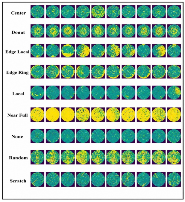
This subsection details the WM811k Silicon Wafer Map Dataset Image dataset [23] employed for training and validating the FGDCNN-WMDDC model. This dataset comprises a subset of the WM811k Silicon Wafer Map Dataset intended for defect classification in semiconductor manufacturing. The dataset is organized into nine defect types and is complemented by a MATLAB implementation of a CNN for defect identification. Defect image contains Center (100), Donut (102), Edge Local (103), Edge Ring (102), Local (100), Near Full (95), None (100), Random (100), Scratch (100). The dataset comprises 902 (sampled subset of WM811k) images. Image format is 32 × 32 pixels .png images. Figure 3 shows the sample images of WM811k Silicon Wafer Map Dataset Image dataset. Table 2 represents dataset evaluation under both 80:20 and 70:30 training/testing split configurations to validate the robustness and generalization capability of the proposed FGDCNN-WMDDC framework.
Figure 4 demonstrates the sample of original images, pre-processed images, and feature map representations.
Figure 3. Sample images of WM811k silicon wafer map dataset image dataset

Figure 4. Sample of original images, preprocessed images, and feature map representations
Table 2. Dataset distribution for training and testing
|
Defect Class |
Total Samples |
80% Training |
20% Testing |
70% Training |
30% Testing |
|
Center |
100 |
80 |
20 |
70 |
30 |
|
Donut |
102 |
82 |
20 |
71 |
31 |
|
Edge Local |
103 |
82 |
21 |
72 |
31 |
|
Edge Ring |
102 |
82 |
20 |
71 |
31 |
|
Local |
100 |
80 |
20 |
70 |
30 |
|
Near Full |
95 |
76 |
19 |
67 |
28 |
|
None |
100 |
80 |
20 |
70 |
30 |
|
Random |
100 |
80 |
20 |
70 |
30 |
|
Scratch |
100 |
80 |
20 |
70 |
30 |
|
Total |
902 |
722 |
180 |
631 |
271 |
4.2 Detailed analysis of results
Several standard classification metrics, such as Overall Success Rate (OSR), Positive Predictive Value (PPV), True Positive Rate (TPR), F-Statistic and G-Measure are used to assess the performance of the proposed FGDCNN-WMDDC framework. The overall classification accuracy of the model is represented by the OSR. PPV is the ratio of the number of correctly predicted positive samples to the total number of positive samples predicted. TPR assesses the sensitivity of the model for detecting real positive samples. F-Statistic is the harmonic mean of precision and recall, and G-Measure is a geometric mean of classification precision and recall. All of these metrics give a complete picture of the effectiveness of classification.
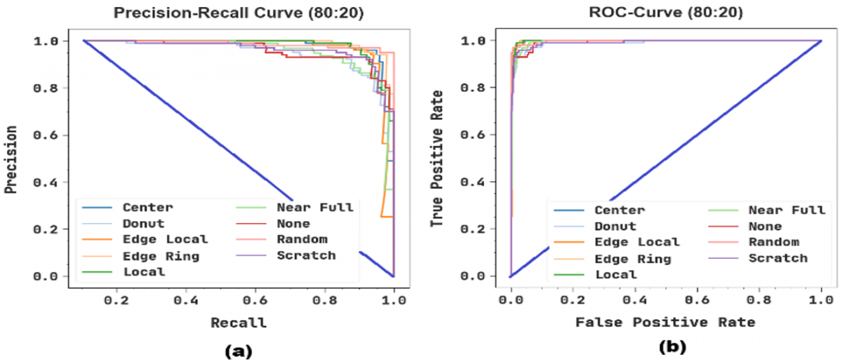
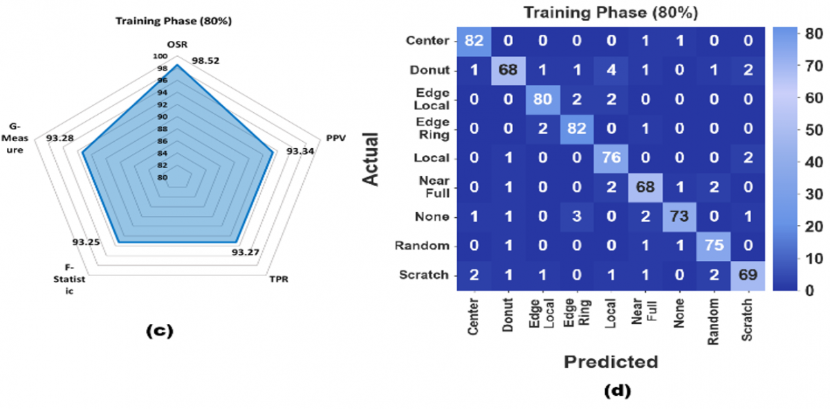
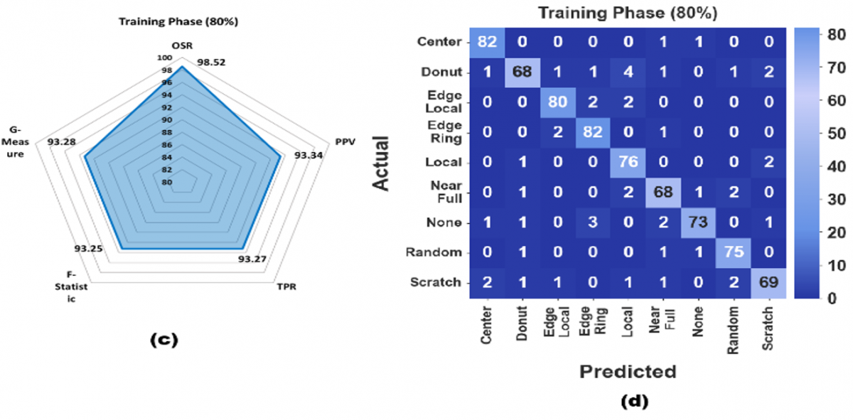
Figure 5 shows the classified outcomes of the FGDCNN-WMDDC approach on 80:20. Figure 5(a) establishes the PR analysis of the FGDCNN-WMDDC method. The outcomes stated that the FGDCNN-WMDDC system results in increasing values of PR. Also, it is noticeable that the FGDCNN-WMDDC model can attain greater PR values on all classes. Consequently, Figure 5(b) demonstrates the Receiver Operating Characteristic (ROC) examination of the FGDCNN-WMDDC system. Subsequently, Figures 5(c) and 5(d) signify the average values and classified results of FGDCNN-WMDDC technique with 80% TRAP from 9 classes.
Figure 6 shows the classified outcomes of the model on 80:20. Figure 6(a) establishes the accuracy analysis of the FGDCNN-WMDDC system. The figure shows that the FGDCNN-WMDDC method attains improved values across increasing epochs. Consequently, Figure 6(b) shows the loss investigation of the FGDCNN-WMDDC method. The outcome shows that the FGDCNN-WMDDC system attains closer values of training and validation loss. Lastly, Figures 6(c) and 6(d) show the average values and classified results of the FGDCNN-WMDDC technique with 20% TESP from 9 classes.
Table 3 demonstrates the classified results of FGDCNN-WMDDC system with 80:20. The outcomes suggest that the FGDCNN-WMDDC model accurately detected the samples. With 80%TRAP, the FGDCNN-WMDDC method provides average values with OSR of 98.52%, PPV of 93.34%, TPR of 93.27%, F-Statistic of 93.25%, and G-Measure of 93.28%, congruently. Simultaneously, with 20% TESP, the FGDCNN-WMDDC model presents average values with OSR of 99.14%, PPV of 96.29%, TPR of 95.99%, F-Statistic of 96.06%, and G-Measure of 96.10%, respectively.
Figure 5. Fine-grained deep convolutional neural network-based wafer map defect detection and classification (FGDCNN-WMDDC) method (a, b) Precision-Recall (PR) and Receiver Operating Characteristic (ROC) curves of 80:20 (c, d) average values and classifier outcomes with TRAP 80%
Table 3. Classifier outcomes of fine-grained deep convolutional neural network-based wafer map defect detection and classification (FGDCNN-WMDDC) method with 80:20
|
Class |
OSR |
PPV |
TPR |
F-Statistic |
G-Measure |
|
Training Phase (80%) |
|||||
|
Center |
99.17 |
95.35 |
97.62 |
96.47 |
96.48 |
|
Donut |
97.78 |
93.15 |
86.08 |
89.47 |
89.54 |
|
Edge Local |
98.89 |
95.24 |
95.24 |
95.24 |
95.24 |
|
Edge Ring |
98.75 |
93.18 |
96.47 |
94.80 |
94.81 |
|
Local |
98.34 |
89.41 |
96.20 |
92.68 |
92.75 |
|
Near Full |
98.20 |
90.67 |
91.89 |
91.28 |
91.28 |
|
None |
98.47 |
96.05 |
90.12 |
92.99 |
93.04 |
|
Random |
98.89 |
93.75 |
96.15 |
94.94 |
94.94 |
|
Scratch |
98.20 |
93.24 |
89.61 |
91.39 |
91.41 |
|
Average |
98.52 |
93.34 |
93.27 |
93.25 |
93.28 |
|
Testing Phase (20%) |
|||||
|
Center |
98.90 |
93.75 |
93.75 |
93.75 |
93.75 |
|
Donut |
97.79 |
91.30 |
91.30 |
91.30 |
91.30 |
|
Edge Local |
98.90 |
90.48 |
100.00 |
95.00 |
95.12 |
|
Edge Ring |
99.45 |
100.00 |
94.12 |
96.97 |
97.01 |
|
Local |
100.0 |
100.00 |
100.00 |
100.00 |
100.00 |
|
Near Full |
98.90 |
95.24 |
95.24 |
95.24 |
95.24 |
|
None |
98.90 |
100.00 |
89.47 |
94.44 |
94.59 |
|
Random |
100.0 |
100.00 |
100.00 |
100.00 |
100.00 |
|
Scratch |
99.45 |
95.83 |
100.00 |
97.87 |
97.89 |
|
Average |
99.14 |
96.29 |
95.99 |
96.06 |
96.10 |

Figure 6. Fine-grained deep convolutional neural network-based wafer map defect detection and classification (FGDCNN-WMDDC) method (a, b) $Accur_y$ and loss curves of 80:20 (c, d) average values and classifier outcomes with TESP 20%

Figure 7. Fine-grained deep convolutional neural network-based wafer map defect detection and classification (FGDCNN-WMDDC) method (a, b) Precision-Recall (PR) and Receiver Operating Characteristic (ROC) curves of 70:30 (c, d) average values and classifier outcomes with TRAP 70%

Figure 8. Fine-grained deep convolutional neural network-based wafer map defect detection and classification (FGDCNN-WMDDC) method (a, b)  and loss curves of 70:30 (c, d) average values and classifier outcomes with TESP 30%
Table 4. Classifier outcomes of fine-grained deep convolutional neural network-based wafer map defect detection and classification (FGDCNN-WMDDC) method with 70:30
|
Class |
OSR |
PPV |
TPR |
F-Statistic |
G-Measure |
|
Training Phase (70%) |
|||||
|
Center |
98.89 |
94.44 |
95.77 |
95.10 |
95.11 |
|
Donut |
98.73 |
93.15 |
95.77 |
94.44 |
94.45 |
|
Edge Local |
98.42 |
92.41 |
94.81 |
93.59 |
93.60 |
|
Edge Ring |
98.89 |
94.67 |
95.95 |
95.30 |
95.30 |
|
Local |
98.26 |
95.00 |
87.69 |
91.20 |
91.27 |
|
Near Full |
98.42 |
91.30 |
94.03 |
92.65 |
92.66 |
|
None |
99.05 |
97.18 |
94.52 |
95.83 |
95.84 |
|
Random |
99.05 |
95.45 |
95.45 |
95.45 |
95.45 |
|
Scratch |
98.26 |
92.42 |
91.04 |
91.73 |
91.73 |
|
Average |
98.66 |
94.00 |
93.89 |
93.92 |
93.94 |
|
Testing Phase (30%) |
|||||
|
Center |
99.26 |
96.55 |
96.55 |
96.55 |
96.55 |
|
Donut |
99.26 |
93.94 |
100.00 |
96.88 |
96.92 |
|
Edge Local |
99.26 |
100.00 |
92.31 |
96.00 |
96.08 |
|
Edge Ring |
98.52 |
92.86 |
92.86 |
92.86 |
92.86 |
|
Local |
99.26 |
100.00 |
94.29 |
97.06 |
97.10 |
|
Near Full |
97.79 |
92.31 |
85.71 |
88.89 |
88.95 |
|
None |
98.52 |
89.66 |
96.30 |
92.86 |
92.92 |
|
Random |
97.05 |
84.21 |
94.12 |
88.89 |
89.03 |
|
Scratch |
97.79 |
93.55 |
87.88 |
90.62 |
90.67 |
|
Average |
98.52 |
93.67 |
93.33 |
93.40 |
93.45 |
Figure 7 shows the classified outcomes of FGDCNN-WMDDC method on 70:30. Figure 7(a) establishes the PR analysis of the FGDCNN-WMDDC technique. The outcomes stated that the FGDCNN-WMDDC model outcomes in enhancing the values of PR. Also, it is noticeable that the FGDCNN-WMDDC approach can attain greater PR values on all classes. Consequently, Figure 7(b) shows the ROC analysis of the FGDCNN-WMDDC system. The figure showed that the FGDCNN-WMDDC model outcome to increased ROC values. Moreover, the FGDCNN-WMDDC technique can extend improved ROC values on all classes. Subsequently, Figures 7(c) and 7(d) show the average values and classified results of the FGDCNN-WMDDC model with 70% TRAP from 9 classes.
Figure 8 demonstrates the classified outcomes of the method on 70:30. Figure 8(a) establishes the accuracy analysis of the FGDCNN-WMDDC technique. The outcomes indicate that the FGDCNN-WMDDC system attains improved values across increasing epochs. Consequently, Figure 8b shows the loss analysis of the FGDCNN-WMDDC method. The outcomes represent that the FGDCNN-WMDDC system attains closer values of training and validation loss. Lastly, Figures 8(c) and 8(d) represent the average values and classified results of FGDCNN-WMDDC model with 30% TESP from 9 classes.
Table 4 displays the classified results of the FGDCNN-WMDDC technique with 70:30. The outcomes suggest that the FGDCNN-WMDDC model accurately detected the samples. With 70%TRAP, the FGDCNN-WMDDC system provides average values with OSR of 98.66%, PPV of 94.00%, TPR of 93.89%, F-Statistic of 93.92%, and G-Measure of 93.94%, respectively. Concurrently, with 30% TESP, the FGDCNN-WMDDC approach provides average values with OSR of 98.52%, PPV of 93.67%, TPR of 93.33%, F-Statistic of 93.40%, and G-Measure of 93.45%, respectively.
The proposed FGDCNN-WMDDC framework managed to obtain high classification results for all categories of wafer defects; however, there were slight differences in results for categories like Edge Local and Near Full. The differences in these patterns are mainly due to the similarity of the visual appearance and overlapping space dimensions of some defect patterns. Moreover, the sample distributions of the minorities can affect discriminative learning capacity for certain classes. However, the combination of PAM and CAM attention mechanisms yields substantial improvements in the localization of the features and reduces inter-class ambiguity, and increases classification robustness.
Table 5. Comparison results of the fine-grained deep convolutional neural network-based wafer map defect detection and classification (FGDCNN-WMDDC) method with existing models
|
Techniques |
OSR |
PPV |
TPR |
F-Statistic |
|
ConvNext |
98.40 |
95.56 |
90.54 |
94.87 |
|
ResNet 50 |
97.80 |
94.87 |
93.63 |
92.51 |
|
AlexNet |
98.20 |
94.90 |
94.57 |
90.25 |
|
EfficientNet-B7 |
96.60 |
95.18 |
94.46 |
94.18 |
|
PeleeNet |
96.41 |
90.78 |
91.77 |
90.37 |
|
SwinTransformer_t |
97.41 |
91.98 |
93.94 |
92.44 |
|
ShuffleNetV2_x1.0 |
95.44 |
93.45 |
93.84 |
93.58 |
|
FGDCNN-WMDDC |
99.14 |
96.29 |
95.99 |
96.06 |
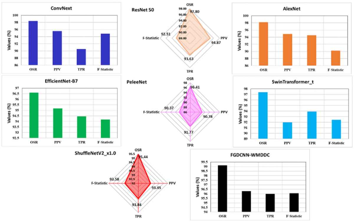
Table 5 and Figure 9 show the comparative results of FGDCNN-WMDDC technique with existing methods [24]. The experimental result inferred that the FGDCNN-WMDDC model has displayed higher performance. The outcome showed that the ShuffleNetV2_x1.0 technique got inefficient performance with OSR of 95.44%, PPV of 93.45%, TPR of 93.84%, and F-Statistic of 93.58%, respectively. Also, the EfficientNet-B7 and PeleeNet methods reach slightly higher results with OSR of 96.60% and 96.41%. Likewise, the SwinTransformer_t method provides somewhat larger performance with OSR of 97.41%, PPV of 91.98%, TPR of 93.94%, and F-Statistic of 92.44%, consistently. Besides, the ResNet 50 technique gives reasonable solution with OSR of 97.80%, PPV of 94.87%, TPR of 93.63%, and F-Statistic of 92.51%, respectively. Concurrently, the ConvNext and AlexNet technique provides closer results with OSR of 98.40% and 98.20%. Lastly, the proposed FGDCNN-WMDDC system accomplishes ensuring solutions with OSR of 99.14%, PPV of 96.29%, TPR of 95.99%, and F-statistic of 96.06%, correspondingly.
Figure 9. Comparison results of fine-grained deep convolutional neural network-based wafer map defect detection and classification (FGDCNN-WMDDC) method with existing systems
The comparative performance analysis shows that the proposed FGDCNN-WMDDC is more effective than the conventional methods in all the performance metrics. The proposed Dual Attention-based feature learning and optimized SSAE classification mechanism is shown to work well through the improvements in OSR, PPV, TPR, and F-Statistic. The uniform superiority of the various experimental setups also suggests the robustness and statistical reliability of the proposed framework.
Table 6. Computational efficiency of the fine-grained deep convolutional neural network-based wafer map defect detection and classification (FGDCNN-WMDDC) approach, compared to existing approaches
|
Models |
FLOPs (M) |
GPU (M) |
Inference Time (ms) |
|
MobileNetV2 |
326.22 |
4072 |
6.80 |
|
MobileNetV3_small |
61.46 |
3128 |
7.16 |
|
MobileViT_XXS |
273.35 |
2355 |
5.08 |
|
ResNet50 |
4131.71 |
2841 |
3.25 |
|
ShuffleNetV2_x1.0 |
151.69 |
4001 |
3.32 |
|
MobileNetV3_large |
233.57 |
2757 |
6.57 |
|
FGDCNN-WMDDC |
10.45 |
784 |
0.95 |
Table 6 shows the computational effectiveness of FGDCNN-WMDDC technique with existing methods. Among the evaluated systems, the proposed FGDCNN-WMDDC model provides minimal FLOP of 10.45M, GPU of 784M, and inference time of 0.95ms, respectively. Also, the MobileNetV2, MobileNetV3_small, MobileViT_XXS, ResNet50, ShuffleNetV2_x1.0, and MobileNetV3_large systems attain maximal results with FLOP, GPU, and prediction time. Thus, the proposed model is found to be an automated tool for detecting silicon wafer map defects.
The results of computational efficiency analysis further validate the applicability of the proposed framework of FGDCNN-WMDDC in the semiconductor manufacturing environment. The obtained lower FLOPs, less GPU memory usage, and negligible inference time highlight the efficiency of the proposed model, making it suitable as an inspection system for wafer defects in real-time applications. Its light weight operational attributes also enable it to be used in automated quality control of industrial applications.
In this manuscript, the FGDCNN-WMDDC model has been presented for detecting and classifying diverse kinds of manufacturing defects in silicon wafers, namely center, donut, edge local, edge ring, local, near full, none, random, and scratch. The FGDCNN-WMDDC approach follows an end-to-end architecture encompassing pre-processing, feature representation, and classification. Primarily, the proposed system applied ABF and contrast enhancement procedure as a pre-processing step. Following that, the Dual Attention EfficientNet architecture is implemented, which can dynamically learn and capture robust classification features. To enhance the performance of the DL method, the hyperparameter selection is carried out through Nadam optimizer. Lastly, SSAE is integrated for the identification and classification of different defect types. The performance validation of the proposed FGDCNN-WMDDC method is examined on WM811k Silicon Wafer Map Dataset Image dataset. Comprehensive experimental results underscored that the proposed method performed better compared to other techniques concerning multiple metrics. Thus, the proposed method can be implemented as an effective tool for automated detection and classification of distinct defects that exist in the wafer map.
The data that support the findings of this study are openly available in Kaggle repository at https://www.kaggle.com/datasets/muhammedjunayed/wm811k-silicon-wafer-map-dataset-image, reference number [23].
[1] Zhou, W., Wang, G.X., Li, Y.F. (2025). Application and development of machine learning in semiconductor manufacturing for automated wafer map pattern recognition and classification. Integration, 107: 102595. https://doi.org/10.1016/j.vlsi.2025.102595
[2] Chandu, H.S., Mathur, S., Gupta, S. (2025). Artificial intelligence-driven approaches for automatic wafer map failure detection in semiconductor manufacturing. In 2025 IEEE International Conference on Interdisciplinary Approaches in Technology and Management for Social Innovation (IATMSI), Gwalior, India, pp. 1-6. https://doi.org/10.1109/iatmsi64286.2025.10985054
[3] Tabatabaeemoshiri, P. (2025). Defects identification on semiconductor wafer for yield improvement using machine learning. Master's thesis, University of Malaya (Malaysia).
[4] Yang, C.J., Chen, Y.H., Hsieh, S.Y. (2025). Enhanced wafer map defect pattern classification through stacking ensemble method and data augmentation integration. The Journal of Supercomputing, 81(5): 643. https://doi.org/10.1007/s11227-025-07113-0
[5] Joo, J., Kim, C.O. (2025). Global feature identification layer for mixed-type wafer bin map classification. Expert Systems with Applications, 271: 126709. https://doi.org/10.1016/j.eswa.2025.126709
[6] Chen, S., Huang, Z., Wang, T., Hou, X., Ma, J. (2025). Wafer map defect recognition based on multi-scale feature fusion and attention spatial pyramid pooling. Journal of Intelligent Manufacturing, 36(1): 271-284. https://doi.org/10.1007/s10845-023-02231-z
[7] Nagamura, Y., Yamanaka, Y., Fujita, I., Arai, M., Fukumoto, S. (2025). Mixed-defect wafer map classification using capsnet-based models with precise scratch-pattern reconstruction. IEEE Access, 13: 182491-182502. https://doi.org/10.1109/access.2025.3621299
[8] Fan, S.K.S., Chen, P.C., Jen, C.H., Sethanan, K. (2024). Auto-labeling for pattern recognition of wafer defect maps in semiconductor manufacturing. Journal of Manufacturing Science and Engineering, 146(7): 070904. https://doi.org/10.1115/1.4065118
[9] Hou, X., Yi, M., Chen, S., Liu, M., Zhu, Z. (2024). Recognition and classification of mixed defect pattern wafer map based on multi-path DCNN. IEEE Transactions on Semiconductor Manufacturing, 37(3): 316-328. https://doi.org/10.1109/tsm.2024.3418520
[10] Singh, N.P., Haldar, A., Pathak, M., Vats, B. (2024). Wafer fault detection in manufacturing using Machine Learning. In 2024 IEEE International Conference on Computer Vision and Machine Intelligence (CVMI), Prayagraj, India, pp. 1-6. https://doi.org/10.1109/cvmi61877.2024.10782617
[11] Rawat, S., Banerjee, D., Gupta, A., Singh, V. (2024). Enhanced prediction of semiconductor wafer defects through CNN forest fusion and random methods for improved efficiency. In 2024 International Conference on Advances in Modern Age Technologies for Health and Engineering Science (AMATHE), Shivamogga, India, pp. 1-6. https://doi.org/10.1109/amathe61652.2024.10582061
[12] Liu, W., Li, G., Cui, Q., Zhang, Z., Wang, X., Bai, C. (2024). Semiconductor wafer particle defect classification based on deep learning and multimodal feature fusion. In 2024 IEEE 12th International Conference on Computer Science and Network Technology (ICCSNT), Dalian, China, pp. 29-34. https://doi.org/10.1109/iccsnt62291.2024.10776716
[13] Lee, H., Kim, H., Kim, H. (2024). Classification of chip-level defect types in wafer bin maps using only wafer-level labels. Journal of Manufacturing Science and Engineering, 146(7): 070902. https://doi.org/10.1115/1.4065226
[14] Lee, C.Y., Pleva, M., Hládek, D., Lee, C.W., Su, M.H. (2025). Ensemble learning for wafer defect pattern classification in the semiconductor industry. IEEE Access, 13: 155714-15572. https://doi.org/10.1109/access.2025.3604405
[15] Taha, K. (2026). Observational and experimental insights into machine learning-based defect classification in wafers. Journal of Intelligent Manufacturing, 37(1): 45-95. https://doi.org/10.1007/s10845-024-02521-0
[16] Altantawy, D.A., Yakout, M.A. (2025). Sparse deep encoded features with enhanced sinogramic red deer optimization for fault inspection in wafer maps. Journal of Intelligent Manufacturing, 36(5): 3359-3397. https://doi.org/10.1007/s10845-024-02377-4
[17] Tsai, T.H., Wang, C.Y. (2025). Wafer map defect classification using deep learning framework with data augmentation on imbalance datasets. EURASIP Journal on Image and Video Processing, 2025(1): 6. https://doi.org/10.1186/s13640-025-00666-3
[18] Souri, A., Mavaddati, S., Gholami, M. (2025). An integrated deep learning model for wafer defect detection using joint spatial and temporal feature representation. Journal of Soft Computing and Information Technology, 1-13.
[19] Kim, M.H., Kim, T.S. (2024). Development of a wafer defect pattern classifier using polar coordinate system transformed inputs and convolutional neural networks. Electronics, 13(7): 1360. https://doi.org/10.3390/electronics13071360
[20] Xie, Y., Li, S., Wu, C.T., Lai, Z., Su, M. (2024). A novel hypergraph convolution network for wafer defect patterns identification based on an unbalanced dataset. Journal of Intelligent Manufacturing, 35(2): 633-646. https://doi.org/10.1007/s10845-022-02067-z
[21] Deng, G., Wang, H. (2024). Efficient mixed-type wafer defect pattern recognition based on light-weight neural network. Micromachines, 15(7): 836. https://doi.org/10.3390/mi15070836
[22] Gavaskar, R.G., Chaudhury, K.N. (2018). Fast adaptive bilateral filtering. IEEE Transactions on Image Processing, 28(2): 779-790. https://doi.org/10.1109/tip.2018.2871597
[23] https://www.kaggle.com/datasets/muhammedjunayed/wm811k-silicon-wafer-map-dataset-image, accessed on Jan. 6, 2026.
[24] Mohammad, F., Ryu, D. (2025). Semiconductor wafer map defect classification with tiny vision transformers. arXiv preprint arXiv:2504.02494. https://doi.org/10.36227/techrxiv.174284964.40200770/v1