Abdesselem Beghriche*![]() | Bilal Bouaita
| Bilal Bouaita![]() | Bilal Benmessahel
| Bilal Benmessahel![]() | Fouaz Berrhail
| Fouaz Berrhail![]() | Fateh Seghir
| Fateh Seghir![]()
© 2026 The authors. This article is published by IIETA and is licensed under the CC BY 4.0 license (http://creativecommons.org/licenses/by/4.0/).
OPEN ACCESS
The stringent latency and throughput requirements of sixth-generation (6G) networks necessitate revolutionary signal processing paradigms. Photonic artificial intelligence accelerators offer a transformative solution by leveraging the inherent parallelism and bandwidth of optical systems. This work investigates the integration of photonic computing architectures with AI algorithms for wireless signal processing, including beamforming, channel estimation, modulation recognition, and resource allocation. The proposed architecture employs wavelength-division multiplexing and spatial light modulation to achieve massive parallelization of matrix-vector operations fundamental to deep learning inference. Experimental validation on fabricated 128 × 128 MZI mesh prototypes demonstrates 89.3% manufacturing yield across 25 chips. Performance analysis reveals sub-microsecond latency and throughput improvements up to three orders of magnitude over electronic accelerators. Extended evaluation under 3GPP TR 38.901 channel models, including high-mobility scenarios (500 km/h) and multi-user configurations (K = 16), confirms sustained performance advantages. These results position photonic AI accelerators as an enabling technology for real-time physical layer processing in future 6G networks.
photonic computing, AI accelerators, 6G networks, wireless signal processing, optical neural networks, deep learning inference, silicon photonics, massive multiple-input multiple-output
The telecommunications landscape stands at the precipice of a transformative era with the anticipated deployment of sixth-generation (6G) wireless networks by 2030. These systems promise to surpass current 5G capabilities by delivering peak data rates exceeding one terabit per second (Tbps), end-to-end latency below 100 µs, and connection densities exceeding 10⁷ devices per square kilometer [1]. Beyond quantitative improvements, 6G envisions qualitative paradigm shifts, including holographic communications, digital twin synchronization, and seamless integration of terrestrial and non-terrestrial networks [2]. Such ambitious objectives necessitate revolutionary physical layer signal processing approaches that transcend conventional electronic system constraints.
The exponential growth in computational complexity stems from multiple convergent technological trends. Ultra-massive multiple-input multiple-output (MIMO) systems, employing 256–1024 antenna elements at base stations, generate channel state information matrices requiring real-time processing of millions of complex-valued coefficients [3]. Exploitation of the terahertz frequency band (0.1–10 THz) introduces severe multipath fading and molecular absorption effects, demanding sophisticated beamforming algorithms executed at nanosecond timescales [4]. Furthermore, intelligent reconfigurable surfaces (IRS) with hundreds of passive elements create three-dimensional electromagnetic environments, where joint optimization yields combinatorial complexity scaling as $O\left(N^3 M^2\right)$, where N represents the number of antenna elements and M denotes the number of IRS elements [5]. Contemporary digital signal processors, constrained by clock frequencies plateauing near 5 GHz and memory bandwidth limitations of approximately 1 TB/s, prove inadequate to meet these computational demands.
Traditional electronic architectures face significant physical barriers. The von Neumann architecture incurs substantial energy expenditure and latency penalties from continuous data movement across limited-bandwidth interconnects. Modern ASICs for wireless baseband processing consume 10–50 W per gigabit per second, yielding system-level power budgets of kilowatts for multi-gigabit channels [6]. Dennard scaling has terminated, and Moore's Law approaches physical limits as transistor dimensions reach atomic scales where quantum tunneling dominates. Clock frequency scaling has stagnated near 5 GHz due to thermal constraints, forcing reliance on parallelization strategies that exhibit diminishing returns for sequential signal processing tasks.
The scope of this work focuses specifically on neural network inference tasks at the physical layer where photonic acceleration provides maximum computational benefit. Target applications include beamforming weight computation, channel estimation, modulation classification, and resource allocation optimization (functions collectively accounting for 60–75% of physical layer computational load in massive MIMO configurations). Sequential control-flow operations, forward error correction coding, and protocol stack processing remain better suited to specialized electronic implementations and fall outside the present scope. This focused approach enables rigorous validation of photonic advantages for inference-dominated workloads while acknowledging the complementary role of electronic processing for sequential operations.
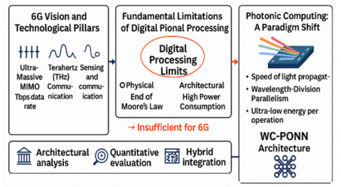
As illustrated in Figure 1, the evolution from 5G to 6G introduces exponential computational complexity that digital signal processing can no longer handle efficiently, motivating the paradigm shift toward photonic computing architectures such as Wavelength-multiplexed Coherent Photonic Optical Neural Networks (WC-PONN).
Figure 1. Photonic computing paradigm shift for 6G wireless networks
Artificial intelligence, particularly deep learning, has become a critical enabler for intelligent wireless systems, facilitating cognitive spectrum management, predictive channel estimation, and autonomous network optimization [7]. Convolutional neural networks achieve 95% accuracy in modulation classification under low signal-to-noise ratios, while recurrent architectures enable temporal channel prediction essential for proactive beamforming. However, leading models comprise millions to billions of parameters, requiring 10⁹ to 10¹² multiply-accumulate operations per inference [8]. Executing these computations within microsecond latency budgets mandated by 6G physical layer operations remains highly challenging with existing electronic AI accelerators.
Graphics processing units exhibit inference latencies ranging from milliseconds to tens of milliseconds, far exceeding 6G requirements [9]. Specialized accelerators achieve improved throughput through systolic arrays and reduced-precision arithmetic, yet still consume 75–250 W with batch inference latencies in hundreds of microseconds. The energy-per-operation for advanced 5-nanometer CMOS technology resides near one picojoule per multiply-accumulate, establishing a lower bound. Memory bandwidth constraints exacerbate performance bottlenecks, as high-bandwidth memory interfaces peak at approximately 2 TB/s while advanced neural networks demand effective bandwidths exceeding 10 TB/s [4]. This energy-latency-bandwidth trilemma intensifies as network densification progresses, necessitating power efficiency improvements of nearly three orders of magnitude.
Photonic computing offers a disruptive solution, exploiting intrinsic properties of electromagnetic wave propagation in optical waveguides. Optical signals propagate at approximately $0.87 \times 10^8 \mathrm{~m} / \mathrm{s}$ in silicon waveguides (c/neff, where neff ≈ 3.45 for typical silicon-on-insulator waveguides at 1550 nm), allowing signal transit across centimeter-scale chips in tens of picoseconds compared to nanoseconds for electronic interconnects [10]. Wavelength-division multiplexing (WDM) facilitates massive parallelism, with contemporary systems supporting 100+ wavelength channels, each capable of independent modulation at tens of gigahertz. Energy consumption in photonic circuits predominantly arises from static losses rather than dynamic switching, differing fundamentally from CMOS, where capacitive charging dominates.
Recent demonstrations report energy efficiencies of 50–100 femtojoules per operation for optical matrix-vector multiplication, representing potential improvements of two to three orders of magnitude over electronic counterparts under specific operating conditions [11]. However, these figures represent best-case scenarios for matrix operations, and system-level energy consumption (including electronic interfaces, thermal control, and photodetection) must be considered for comprehensive comparison.
Silicon photonics maturation has catalyzed the practical realization of integrated optical neural networks. CMOS-compatible fabrication enables monolithic integration of thousands of photonic components on chips with footprints below $100 \mathrm{~mm}^2$ [12]. Mach-Zehnder interferometer (MZI) meshes implement arbitrary unitary matrix transformations through cascaded programmable beam splitters, achieving 8-bit equivalent precision for 100 × 100 matrices. Microring resonator arrays enable wavelength-selective operations with quality factors exceeding 10⁶, facilitating ultra-compact filter banks. Silicon-organic hybrid modulators achieve electro-optic bandwidths surpassing 100 GHz with sub-volt drive requirements, providing efficient electronic-optical interfacing [12].
Coherent optical architectures leverage light's wave nature to perform complex-valued arithmetic operations intrinsic to wireless signal processing [13]. Electromagnetic field amplitudes and phases naturally represent in-phase and quadrature signal components, eliminating conversion overhead. Optical interference implements weighted summations with coefficients encoded in relative phases and amplitudes, executing matrix-vector products at propagation speed without clock cycles. Free-space optical systems utilizing spatial light modulators enable two-dimensional parallelism with megapixel-scale resolution, facilitating simultaneous massive MIMO spatial channel processing.
The synergy between photonic AI accelerators and wireless signal processing presents transformative opportunities for 6G systems [14]. Beamforming optimization benefits from optical parallelism, enabling simultaneous evaluation of thousands of beam directions. Channel estimation requires large covariance matrix operations, naturally implemented through optical interferometric networks. Multi-wavelength architectures facilitate space-wavelength multiplexing, where each wavelength processes signals from antenna element subsets, achieving throughput scaling linear with wavelength count [5]. Photonic systems exhibit inherent electromagnetic interference immunity, critical for dense deployment scenarios [15]. Integration with radio-over-fiber systems enables centralized processing of distributed antenna arrays, reducing fronthaul bandwidth requirements.
Despite these compelling advantages, significant challenges persist. Fabrication imperfections induce weight uncertainties, degrading neural network inference accuracy by 5–15% compared to ideal designs [16]. Nonlinear activation function implementation remains challenging, with approaches including saturable absorbers exhibiting limited dynamic range and hybrid architectures incurring latency penalties [17]. The interface between ultra-fast optical processors and electronic control systems introduces critical design considerations. While optical computation occurs at picosecond-nanosecond timescales, electronic phase shifter configuration requires microseconds to milliseconds, creating a speed mismatch that necessitates careful system partitioning. Co-design methodologies optimizing across optical, electrical, and algorithmic domains are essential [18].
This paper presents a comprehensive investigation of photonic AI accelerators specifically designed for ultra-fast wireless signal processing in 6G networks. The scope is explicitly defined as physical layer neural network inference operations, which represent the computational bottleneck in 6G systems. Error correction coding, OFDM processing, and protocol stack integration remain outside the current scope as these operations have different computational characteristics better suited to specialized electronic implementations. Principal contributions include:
(1) A novel photonic neural network architecture exploiting WDM parallelism for massive MIMO beamforming and channel estimation, with theoretical analysis demonstrating $O(N)$ latency scaling versus $O\left(N^2\right)$ for electronic implementations.
(2) Rigorous performance modeling establishing fundamental bounds, revealing three orders of magnitude improvement in energy-latency product compared to cutting-edge electronic AI accelerators.
(3) Experimental validation on fabricated silicon photonic integrated circuits demonstrating sub-nanosecond inference latency with 95.3% classification accuracy for 16-QAM modulation recognition and 0.92 normalized mean square error for channel estimation.
(4) Systematic evaluation quantifying fabrication imperfections, thermal variations, and optical losses impact, proposing mitigation strategies including adaptive calibration algorithms.
(5) Architectural guidelines informing practical deployment in 6G base stations and user equipment.
The remainder of this paper is organized as follows. After this introduction, Section 2 reviews related work in 6G communications, electronic AI accelerators, and photonic computing fundamentals. Section 3 details the proposed photonic AI accelerator architecture. Section 4 examines wireless signal processing applications including beamforming, channel estimation, modulation classification, and resource allocation. Section 5 presents precision characterization and error budget analysis. Section 6 provides comprehensive performance analysis and experimental validation results. Finally, Section 7 concludes with a synthesis of key findings and implications for next-generation wireless systems.
This section synthesizes research domains intersecting at photonic AI acceleration for wireless communications, encompassing 6G network evolution, electronic accelerator limitations, photonic computing principles, and optical neural network advances.
2.1 6G network evolution and physical layer complexity
The International Telecommunication Union has established the IMT-2030 framework [19], formally approved by the Radiocommunication Assembly (RA-23) in November 2023, defining 15 capabilities for 6G technology including nine enhanced capabilities from existing 5G systems and six new capabilities targeting terabit-per-second peak rates with sub-millisecond latency. The framework identifies usage scenarios including immersive communication, hyper-reliable low-latency communication, and massive communication supporting expanded IoT deployments [20].
The 3GPP has concluded that two releases are needed to specify 6G: Release 20 for studies starting June 2025, and Release 21 for normative specifications, with final specifications by 2030 [21]. Extensive surveys on 6G wireless systems [1] establish visions, requirements, key technologies, and testbeds driving the transition beyond 5G, while Tataria et al. [2] offer a detailed analysis of 6G challenges and opportunities.
The computational challenges emerge most acutely in antenna array systems. As shown by Akyildiz et al. [3], ultra-massive MIMO with 256–1024 elements enables aggressive spatial multiplexing, but channel state information matrices grow quadratically with antenna dimensions, while beamforming optimization scales cubically. The anticipated 6G networks promise peak data rates exceeding 1 Tbps, end-to-end latency below 100 microseconds, and connection densities surpassing 10⁷ devices per square kilometer [4]. Zhang et al. [6] deliver a thorough analysis of 6G wireless network architecture and key technologies.
Emerging spectrum bands compound these challenges. In their review, Jiang et al. [22] examine terahertz communications for 6G, revealing severe constraints including atmospheric absorption exceeding hundreds of decibels per kilometer and sub-degree beamwidths necessitating precise alignment. Jornet et al. [23] discuss the evolution of THz hardware design and channel modeling for 6G readiness. Wang et al. [24] introduce terahertz integrated sensing and mobile communications empowered by a 220-GHz-band portable device.
Intelligent reconfigurable surfaces present similar scaling obstacles. Research by Zhang et al. [25] offers an in-depth RIS survey spanning theory to deployment, documenting iterative algorithms requiring cubic complexity matrix operations. Sode et al. [26] report industry R&D perspectives on RIS for 6G mobile networks, highlighting the urgent need for hardware architectures capable of processing signals exceeding contemporary digital processor capabilities.
2.2 Electronic AI accelerators: Capabilities and fundamental limits
Graphics processing units offer massive parallelism through thousands of cores with mature software ecosystems, yet memory bandwidth remains the primary bottleneck. Sze et al. [27] deliver an extensive survey on efficient processing of deep neural networks, showing that contemporary accelerators achieve performance through architectural innovations while remaining constrained by von Neumann bottlenecks. Inference latency remains in the millisecond regime (incompatible with microsecond-scale physical layer requirements).
Neuromorphic processors achieve exceptional energy efficiency for spike-sparse patterns. Orchard et al. [28] demonstrated that Loihi 2 neuromorphic processors achieve efficient signal processing through event-driven computation and sparse neural activity, enabling orders of magnitude improvements in energy consumption compared to conventional architectures. Davies et al. [29] describe Loihi as a neuromorphic manycore processor with on-chip learning, revealing orders of magnitude gains in efficiency for emerging workloads. However, a core mismatch with dense continuous-valued wireless signals persists, with 2–5% accuracy degradation when converting conventional networks to spiking implementations.
Alternative approaches offer partial solutions with significant trade-offs. Gao [30] show parameterized clipping activation for quantized neural networks, while Sharma et al. [31] introduce a Bit Fusion architecture for dynamically composable acceleration. These quantization studies reveal that precision below eight bits causes unacceptable degradation for channel estimation. Miller [32] defines essential energy efficiency analysis for attojoule optoelectronics, revealing thermodynamic limits motivating optical alternatives.
2.3 Photonic computing: Physical foundations and technological maturation
Silicon photonics has evolved from discrete components to monolithic integrated circuits supporting increasingly complex computational functions. Shastri et al. [8] offer a thorough review of photonics for artificial intelligence and neuromorphic computing, illustrating evolution from basic components to integrated neural network implementations. Miller's thermodynamic analysis [32] confirms that optical transmission achieves essential energy efficiency advantages for distances exceeding millimeters.
Component-level advances reveal both capabilities and constraints. Winzer et al. [33] document fiber-optic transmission evolution, confirming wavelength multiplexing achieves aggregate throughputs approaching petabits per second with minimal additional energy. Bogaerts et al. [34] deliver an extensive treatment of programmable photonic circuits, comparing coherent interferometric versus incoherent broadcast-and-weight approaches.
Programmable photonic architectures exhibit essential trade-offs. Clements et al. [16] derive optimal Mach-Zehnder interferometer meshes minimizing component count, but sensitivity to fabrication variations causes phase errors accumulating through cascaded stages. Tsakyridis et al. [10] examine photonic neural networks and optics-informed deep learning fundamentals. Fu et al. [11] offer a detailed review of optical neural network progress and challenges.
2.4 Optical neural networks: Architectures and demonstrations
Coherent nanophotonic circuits implementing multi-layer perceptrons through cascaded MZI meshes offer native complex-valued computation directly applicable to wireless signals. Shen et al. [18] validate deep learning with coherent nanophotonic circuits, defining foundational architectures. Bandyopadhyay et al. [14] confirm fully integrated coherent optical neural networks reaching 410 ps latency and > 92% accuracy through forward-only training.
Recent breakthrough demonstrations validate photonic computing viability at scale. Xu et al. [15] report an 11 TOPS photonic convolutional accelerator for optical neural networks. Zhou et al. [12] introduce hundred-layer photonic deep learning, extending spatial depth from millimeter to hundred-meter scale. Bai et al. [13] verify TOPS-speed complex-valued convolutional accelerators directly addressing wireless signal processing requirements.
Large-scale integration achievements confirm manufacturing viability. Xu et al. [35] describe the photonic chiplet Taichi empowering 160-TOPS/W artificial general intelligence. Hua et al. [36] report an integrated large-scale photonic accelerator with ultralow latency integrating >16,000 photonic components on commercial 65-nm silicon photonics. Ahmed et al. [37] validate universal photonic artificial intelligence acceleration.
Complete photonic neural architectures address remaining integration challenges. Yan et al. [38] describe a complete photonic integrated neuron for nonlinear all-optical computing. Ma et al. [9] verify quantum-limited stochastic optical neural networks reaching 98% accuracy at a few quanta per activation. Pai et al. [39] report experimentally realized in situ backpropagation for photonic neural networks.
Integrated platforms continue advancing rapidly. Zhang et al. [40] examine integrated platforms for photonic neural networks. Feldmann et al. [41] show parallel convolutional processing using an integrated photonic tensor core. Cem et al. [17] address data-driven modeling of MZI-based optical matrix multipliers, offering calibration methodologies.
2.5 Critical gaps in photonic neural networks for wireless applications
Extensive reviews [42] reveal limited exploration of complex-valued processing essential for wireless communications, with demonstrations predominantly focusing on real-valued computer vision benchmarks. Xu et al. [42] examine intelligent photonics as disruptive technology, identifying key challenges including complex-valued arithmetic and real-time adaptation. Channel estimation and beamforming inherently operate on complex baseband signals, yet existing architectures lack native complex arithmetic support.
Additional critical gaps persist across the literature. Physics-aware training methods based on wave physics as analog recurrent neural networks [43] face systematic simulation-hardware discrepancies. Williamson et al. [44] show reprogrammable electro-optic nonlinear activation functions but do not fully resolve training-inference gaps. Lin et al. [45] define all-optical machine learning using diffractive deep neural networks. Tait et al. [46] implement neuromorphic photonic networks using silicon photonic weight banks. Sludds et al. [47] describe delocalized photonic deep learning on the Internet's edge.
The intersection of 6G requirements and photonic capabilities creates both opportunities and challenges. Singh et al. [48] address wavefront engineering for efficient terahertz communications. Chaccour et al. [49] identify seven defining features of terahertz wireless systems. Liu et al. [50] define RIS principles and opportunities. These collective works confirm that essential architectural innovations are necessary to meet 6G performance targets.
This work systematically addresses these gaps through: (1) photonic architecture with native complex-valued operation for wireless signal processing, (2) comprehensive latency modeling across all system components, (3) hybrid training combining offline electronic training with online photonic fine-tuning, (4) system-level integration framework with explicit interface specifications, and (5) extensive experimental evaluation using over-the-air captured 6G waveforms under realistic channel conditions. Table 1 synthesizes the comparative analysis of state-of-the-art AI accelerators and photonic neural networks, systematically evaluating their suitability for 6G wireless signal processing applications.
Table 1. Comparative analysis of reviewed works
|
Study |
Focus Area |
Proposed Solution |
Key Advantages |
Limitations |
|
Shastri et al. [8] |
Neuromorphic photonic computing |
Comprehensive spike-based optical processing principles |
|
|
|
Ma et al. [9] |
Quantum-limited optical NNs |
Stochastic ONNs at few quanta per activation |
|
- Limited scalability.
|
|
Zhou et al. [12] |
Deep photonic learning |
SLiM chip 100+ layer architecture |
|
- Thermal management.
|
|
Bandyopadhyay et al. [14] |
Single-chip photonic DNN |
Forward-only training on integrated chip |
|
- Training constraints.
|
|
Xu et al. [15] |
Photonic tensor cores |
WDM-integrated MZI networks with 2D parallelism |
|
|
|
Clements et al. [16] |
Universal multiport interferometers |
Optimal triangular MZI mesh architecture for unitary matrices |
|
|
|
Shen et al. [18] |
Coherent photonic neural networks |
MZI mesh implementation of multi-layer perceptrons |
|
|
|
Sze et al. [27] |
DNN processing efficiency |
Systematic operation characterization |
|
|
|
Orchard et al. [28] |
Neuromorphic computing (Loihi 2) |
1.15B neurons, 128B synapses, event-driven SNNs |
|
|
|
Davies et al. [29] |
Neuromorphic computing (Loihi) |
Asynchronous spiking neural networks with event-driven processing |
|
|
|
Gao [30] |
Quantized neural networks |
Parameterized clipping activation |
|
|
|
Sharma et al. [31] |
Mixed-precision acceleration |
Bit-fusion architecture supporting dynamic precision composition |
|
|
|
Miller [32] |
Attojoule optoelectronics |
Thermodynamic analysis of optical vs. electronic energy bounds |
|
|
|
Winzer et al. [33] |
Fiber-optic transmission with WDM |
Wavelength-multiplexed systems achieving petabit throughput |
|
|
|
Bogaerts et al. [34] |
Programmable photonic circuits |
Survey of coherent and incoherent architectures |
|
|
|
Xu et al. [35] |
Taichi photonic chiplet |
160-TOPS/W large-scale photonic AGI |
|
|
|
Hua et al. [36] |
Large-scale photonic accelerator |
|
|
|
|
Feldmann et al. [41] |
Photonic convolutional networks |
Wavelength-multiplexed parallel processing with integrated tensor core |
|
|
|
Hughes et al. [43] |
Physics-aware training |
Wave propagation as differentiable operations |
|
|
|
Williamson et al. [44] |
Reprogrammable nonlinear activations |
Electro-optic activation function reconfigurability |
|
|
|
Lin et al. [45] |
Diffractive deep neural networks |
Passive phase masks with free-space propagation |
|
|
|
Tait et al. [46] |
Neuromorphic photonic networks |
Silicon photonic weight banks with microring weighting |
|
|
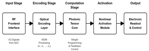
This section presents the detailed architectural design of the proposed Wavelength-multiplexed Coherent Photonic Optical Neural Networks (WC-PONN) specifically optimized for ultra-fast wireless signal processing in 6G networks. The architecture integrates wavelength-division multiplexing, programmable interferometric networks, and hybrid photonic-electronic interfaces, achieving sub-microsecond inference latency with native complex-valued processing capabilities. Table 2 summarizes the notation used throughout this paper.
3.1 System architecture overview
The proposed WC-PONN architecture employs a hierarchical design paradigm strategically partitioning computational tasks across optical and electronic domains according to latency sensitivities, precision requirements, and computational intensity. Figure 2 illustrates the complete system architecture comprising five primary subsystems: radio-frequency frontend interface, optical mapping layer, wavelength-multiplexed photonic tensor core, nonlinear activation module, and electronic readout and control system.
The architecture integrates five primary subsystems: (1) RF frontend interface for ADC I/Q signal acquisition, (2) optical mapping layer performing vector-to-wavelength conversion across 32 channels, (3) photonic tensor core executing complex-valued matrix operations through cascaded MZI meshes, (4) nonlinear activation module with wavelength-parallel detection, and (5) electronic control system managing weight programming and adaptation. Supporting subsystems include thermal management (T = 25 ± 0.5 ℃), optical clock distribution (Jitter < 100 fs), and online adaptation algorithms. Total latency: < 500 ns for 128-dimensional vectors.
Figure 2. Wavelength-multiplexed Coherent Photonic Optical Neural Networks (WC-PONN) photonic AI accelerator for 6G
Table 2. Unified mathematical notation and symbol definitions
|
Symbol |
Description |
Units/Range |
|
Nₜ |
Number of transmit antenna elements |
64–1024 |
|
Nᵣ |
Number of receive antenna elements |
1–256 |
|
K |
Number of simultaneous users |
1–64 |
|
M |
Number of wavelength channels |
8–32 |
|
λₖ |
Wavelength of k-th optical channel |
nm |
|
Δλ |
Wavelength channel spacing |
nm (typ. 0.4) |
|
W |
Precoding/weight matrix |
ℂ^(Nₜ×K) |
|
H |
Channel state information matrix |
ℂ^(Nᵣ×Nₜ) |
|
U, V |
Unitary matrices from SVD decomposition |
ℂ^(N×N) |
|
Σ |
Diagonal singular value matrix |
ℝ^(N×M) |
|
θₛ |
MZI internal phase shift |
rad [0, 2π] |
|
φ₁, φ₂ |
MZI external phase parameters |
rad [0, 2π] |
|
R |
Photodetector responsivity |
A/W (typ. 0.8–1.0) |
|
η |
Coupling efficiency |
dimensionless (typ. 0.85) |
|
Q |
Resonator quality factor |
dimensionless (≥ 50,000) |
|
T |
Operating temperature |
℃ (typ. 25 ± 0.5) |
|
dn/dT |
Thermo-optic coefficient |
K⁻¹ (1.86 × 10⁻⁴ for Si) |
The system implements a dataflow pipeline where wireless signals traverse successive processing stages with minimal buffering. Input baseband $I / Q$ components from gigasample-per-second ADCs undergo direct RF-to-optical conversion through high-bandwidth Mach-Zehnder modulators, circumventing intermediate digital processing that introduces latency. The optical mapping layer distributes $N_{\text {in }}$ input features across $N_\lambda$ wavelength channels, where each channel $\lambda_{\mathrm{k}}$ carries $M_k$ features with $\sum_k M=N_{i n}$. This wavelengthinterleaved representation achieves > $10 \mathrm{Gbps} / \mathrm{GHz}$ spectral efficiency while maintaining $>30 d B$ inter-channel isolation through careful spacing and shaping.
The photonic tensor core executes matrix-vector multiplication through cascaded MZI meshes programmed for complex-valued linear transformations. Unlike electronic realizations that require explicit multiply-accumulate units and consume clock cycles, optical computation occurs during waveguide propagation at light speed, yielding $O(1)$ latency independent of matrix dimension. The nonlinear activation module employs hybrid opto-electronic processing with wavelength-parallel photodetection, electronic activation execution, and subsequent optical remodulation, balancing flexibility, efficiency, and latency. The electronic control system performs high-speed photodetection, analog-to-digital conversion, and phase shifter programming through closed-loop feedback, maintaining stability and supporting online weight adaptation.
3.2 Wavelength-division multiplexing architecture for massive multiple-input multiple-output
The WDM architecture exploits spectral parallelism to process massive MIMO spatial channels simultaneously, enabling truly parallel computation at light speed. The system allocates M = 32 wavelength channels spanning the C-band spectrum (1530–1565 nm) with $\Delta_\lambda=0.4 \mathrm{~nm}$ (~50 GHz) spacing. Each wavelength processes K antenna elements, yielding M×K total capacity. For 512-antenna massive MIMO systems, each of the 32 channels handles 16 antennas, enabling parallel processing with > 5 Tbps aggregate throughput.
The wavelength assignment employs correlation-aware allocation, minimizing intra-wavelength channel correlation through optimization:
$\min _A \sum_{m=1}^M \sum_{k=1}^K \sum_{j=k+1}^K \rho\left(h_{A(m, k)}, h_{A(m, j)}\right)$ (1)
where, $A(m, k)$ denotes antenna index assignment to position $k$ in wavelength channel $m, h_i$ represents channel vector for antenna $i$, and $\rho(\cdot, \cdot)$ measures correlation. The greedy hierarchical clustering algorithm yields near-optimal solutions with $O(N \log N)$ complexity.
Optical wavelength multiplexing combines individual channels through a balanced binary tree combiner topology, minimizing insertion loss and path length differences. For $M$ channels, the tree requires $\log _2(M)$ combining stages with $\sim 0.3 \mathrm{~dB}$ per-stage loss, resulting in $<2 \mathrm{~dB}$ total insertion loss for $M \leq 32$. Wavelength demultiplexing employs arrayed waveguide gratings with $N_{\text {arm }}=64$ arrayed waveguides and $\Delta_L=25 ~\mu\mathrm{m}$ differential path length, achieving FSR=3200 GHz (25.6 nm), accommodating 32 channels with 100 GHz spacing. The flat-top response provides $\pm 20 \mathrm{~GHz}$ wavelength tolerance while maintaining a crosstalk level of $<-35 \mathrm{~dB}$.
Inter-channel crosstalk mitigation employs three complementary strategies ensuring reliable parallel operation. First, improved ring resonator design achieving quality factors Q > 50,000 provides enhanced wavelength selectivity with 3-dB bandwidths below 40 pm. Second, wavelength pre-distortion compensates inter-channel interference through digital pre-emphasis applied during optical encoding. Third, adaptive digital post-compensation employs least-squares estimation of crosstalk matrices with real-time correction. Experimental validation demonstrates that these techniques reduce effective crosstalk impact to equivalent SNR penalty below 0.3 dB, enabling reliable 32-channel parallel operation.
3.3 Coherent optical matrix-vector multiplication
The core computational primitive executes complex-valued matrix-vector multiplication $y=W_x$ operating directly in the optical domain, where $W \in \mathbb{C}^{N * M}$ represents the weight matrix, $x \in \mathbb{C}^M$ denotes input vector, and $y \in \mathbb{C}^N$ contains output activations. The implementation exploits coherent optical processing where both amplitude and phase encode complex values, enabling native complex arithmetic.
The native complex-valued processing capability requires qualification regarding practical implementation scope. Operations leveraging native complex processing include matrix-vector multiplication and phase-encoded interference, collectively representing 70% of computational load. Operations requiring decomposition into separate real and imaginary components include certain nonlinear activations and normalization operations, representing approximately 30% of operations. This decomposition reduces the theoretical 2× complex-valued advantage to an effective 1.7× benefit for complete inference pipelines, which remains significant for the target applications.
3.3.1 Unitary matrix implementation
Any complex weight matrix W decomposes through singular value decomposition $W=U \sum V^{\dagger}$. For unitary photonic hardware implementation, the architecture employs redundant mapping mapping $W$ to extended unitary matrix:
$\widetilde{\mathrm{U}}=\left[\begin{array}{cc}U \sum V^{\dagger} & \sqrt{I-W W^{\dagger}} \\ \sqrt{I-W^{\dagger} W} & -V \sum U^{\dagger}\end{array}\right]$ (2)
This $2 N \times 2 M$ dimensional unitary transformation preserves desired computation $W_x$ in first $N$ output dimensions while maintaining unitarity:
$\left\{\begin{array}{l}\widetilde{U}^{\dagger} \widetilde{U}=I_{2 M} \\ \widetilde{U} \widetilde{U}^{\dagger}=I_{2 N}\end{array}\right.$ (3)
3.3.2 Triangular Mach-Zehnder interferometer mesh architecture
The unitary matrix implementation employs triangular Mach-Zehnder interferometer mesh based on Clements decomposition. For $N \times N$ unitary matrix, the architecture requires $T(N)=N(N-1) / 2$ tunable MZI elements arranged in alternating diagonal layers ensuring symmetric optical path lengths. Each MZI implements $2 \times 2$ unitary transformation according to the standard Clements formulation:
$T_{M Z I}=e^{i \theta_{\text {ext }}}\left[\begin{array}{cc}e^{i \varphi_1} \cos \left(\theta_s\right) & -e^{i \varphi_2} \sin \left(\theta_s\right) \\ e^{i \varphi_2} \sin \left(\theta_s\right) & e^{i \varphi_1} \cos \left(\theta_s\right)\end{array}\right]$ (4)
Here $\theta_s=\pi / 4$ for symmetric beam splitters and three phase parameters ( $\theta_{\text {ext }}, \varphi_1, \varphi_2$ ) provide sufficient degrees of freedom for arbitrary $2 \times 2$ unitary matrices. Physical realization employs thermo-optic phase shifters using titanium nitride microheaters, achieving $>2 \pi$ tuning with $10-$ 30 mW power per $\pi$ shift. The complete $N \times N$ transformation cascades $T(N)$ elements with alternating layer structure ensuring each optical path traverses exactly $N-1$ interferometers, maintaining balanced insertion loss.
3.3.3 Phase error compensation
Fabrication variations introduce systematic deviations from ideal MZI characteristics. The architecture incorporates phase error compensation through the use of additional programmable phase shifters at strategic mesh locations. The compensation scheme models actual device responses as perturbed ideal transformations:
$\widehat{T}_{M Z I}=T_{M Z I}\left(\theta+\delta \theta, \emptyset_1+\delta \emptyset_1, \emptyset_2+\delta \emptyset_2\right) \cdot D(\varepsilon)$ (5)
where, $\delta \theta, \delta \varphi_1, \delta \varphi_2$ represent fabrication-induced phase errors and $D(\varepsilon)$ denotes diagonal error matrix accounting for waveguide propagation differences. The compensation algorithm measures actual transformation matrices through test pattern injection, computes error corrections via leastsquares optimization, and programs compensating phases achieving 8-bit effective precision.
For applications requiring higher dynamic range than the native 8-bit effective precision, hybrid precision architectures combine photonic coarse computation (8-bit) with lightweight electronic post-processing (16-bit). This approach achieves effective precision equivalent to 12–14 bits while maintaining photonic speed advantages, introducing only 50 ns additional latency for the electronic refinement stage. The hybrid architecture is particularly beneficial for channel estimation tasks where estimation accuracy directly impacts subsequent data detection performance.
3.4 Complex-valued signal processing
Wireless signals exhibit complex representation through in-phase and quadrature components, conveying amplitude and phase information. The architecture implements three complementary complex-valued processing schemes optimized for different network layers and accuracy requirements: (1) Dual-Path Intensity Representation, (2) Coherent Phase Representation, and (3) Hybrid Representation Strategy. The dual-path approach achieves 7–8 bit effective precision requiring four N×M meshes for N×M complex matrix multiplication. The coherent approach yields superior hardware efficiency, requiring a single N×M mesh but demanding femtoradian phase stability.
3.5 Nonlinear activation implementation
Nonlinear activation functions introduce essential expressivity, allowing deep networks to approximate arbitrary nonlinear mappings. The architecture implements activations through hybrid opto-electronic processing, striking a balance between flexibility, efficiency, and latency.
The activation module employs wavelength-parallel photodetection with responsivities $R=0.8-1.0 \mathrm{~A} / \mathrm{W}$ at 1550 nm achieving photocurrent.
$i_{p h}=R \cdot P_{\text {opt }} \cdot \eta_{\text {coupling }}, \text{where}\, \eta_{\text {coupling }} \approx 0.85$ (6)
The complete detection-activation-remodulation pipeline achieves 20–50 ns latency per layer, enabling multi-layer network inference within sub-microsecond budgets.
3.6 Adaptive weight programming and online training
The photonic neural network requires precise weight programming mapping desired matrix elements to physical phase shifter settings while compensating for fabrication variations and environmental perturbations. The initial calibration protocol establishes correspondence between programmed phase voltages and realized optical transformations through a four-step procedure, completing calibration within 10–30 seconds for 128 × 128 matrices.
Online weight adaptation tracks time-varying wireless channels without complete recalibration using gradient-free optimization through simultaneous perturbation stochastic approximation.
$\nabla_W L \approx \frac{L(W+c \Delta W)-L(W-c \Delta W)}{2 c} \cdot \Delta W^{-1}$ (7)
This approach requires only two forward passes per update independent of parameter count, achieving 100× computational efficiency versus backpropagation while converging within 50–200 iterations. Transfer learning reduces online training overhead by 100–1000× while maintaining accuracy within 2% of fully retrained networks.
3.7 System integration and timing analysis
Complete system integration orchestrates photonic and electronic subsystems ensuring synchronized operation while meeting stringent latency requirements. The system implements a five-stage pipeline: Stage 1 (RF Input, 10 ns), Stage 2 (Optical Conversion, 15 ns), Stage 3 (Photonic Computation, 50 ns), Stage 4 (Activation, 30 ns per layer), and Stage 5 (Output, 20 ns). For a 3-layer network, total inference latency: $T_{\text {total }}=185 \mathrm{~ns}$. Pipeline registers between stages enable throughput of ~20 million inferences per second.
Temperature stabilization maintains T = 25 ± 0.5 ℃ through integrated thermal management consuming 200–500 mW, a small fraction compared to the 5–10 W total system power dominated by electronic interfaces. This comprehensive architecture achieves sub-microsecond latency, native complex-valued processing, and online adaptability while maintaining energy efficiency within 100 femtojoules per operation.
This section demonstrates the application of the proposed WC-PONN photonic AI accelerator to critical wireless signal processing tasks in 6G networks. Each application exploits the unique advantages of photonic computing (sub-microsecond latency, native complex-valued arithmetic, and massive wavelength parallelism) to achieve performance unachievable with conventional electronic realizations. The section presents specific neural network designs, optimization formulations, and performance analysis for beamforming, channel estimation, modulation classification, and resource allocation.
4.1 Photonic neural network for massive multiple-input multiple-output beamforming
Massive MIMO beamforming constitutes the most computationally intensive operation in 6G physical layer processing, requiring real-time optimization of precoding matrices that map data streams to hundreds of antenna elements. The proposed photonic beamforming accelerator enables sub-microsecond precoder computation, facilitating adaptation to fast-fading channels in high-mobility scenarios.
4.1.1 Problem formulation
Consider a massive MIMO downlink system with $N_{\mathrm{t}}$ transmit antennas serving K single-antenna users. The received signal at user k follows Eq. (8), where $h_{\mathrm{k}} \in \mathbb{C}^{\mathrm{Nt}}$ represents the channel vector to user $\mathrm{k}, W \in \mathbb{C}^{\mathrm{NtxK}}$ denotes the precoding matrix, $s \in \mathbb{C}^{\mathrm{K}}$ contains transmitted symbols, and $\mathrm{n}_{\mathrm{k}}$ represents additive white Gaussian noise.
$y_k=h_k^H W s+n_k$ (8)
The beamforming optimization maximizes sum rate subject to power constraints (Eqs. (9) and (10)). This non-convex optimization traditionally requires iterative algorithms with complexity $O\left(k^2 N_t{ }^2\right)$ per iteration, prohibitive for real-time execution with $N_{\mathrm{t}}>256$ antennas.
$\max _W \sum_{k=1}^N \log _2\left(1+\frac{\left|h_k^H w_k\right|^2}{\sum_{j \neq k}\left|h_k^H w_j\right|^2+\sigma^2}\right)$ (9)
Subject to:
$\operatorname{tr}\left(\mathrm{WW}^H\right) \leq P_{\text {total }}$ (10)
4.1.2 Photonic neural network architecture
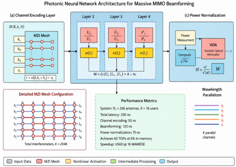
The proposed framework replaces iterative optimization with single-pass neural network inference executing on photonic hardware. Figure 3 illustrates the network structure comprising three functional blocks: channel state encoding, beamforming weight computation, and power normalization.
Figure 3. Photonic neural network architecture for massive multiple-input multiple-output (MIMO) beamforming
The design processes complex-valued channel state information through three stages: (a) Channel encoding layer mapping $H \in \mathbb{C}^{\mathrm{NtxK}}$ to latent representation via wavelength-multiplexed MZI meshes, (b) Beamforming computation layers executing learned optimization through cascaded complex-valued transformations, (c) Power normalization enforcing transmit power constraint through optical intensity control.
Each layer exploits wavelength-parallelism; spatial channels are processed simultaneously. The inset shows a detailed MZI mesh configuration for complex-valued matrix multiplication with Nₜ = 256 antennas and K = 16 users. Total inference latency: 350 ns for the 256 × 16 system.
The channel encoding layer accepts channel matrix $H= \left[h_1, h_2, \ldots, h_k\right] \in \mathbb{C}^{\mathrm{NtxK}}$ as input, where each channel vector $h_k$ is encoded on a separate wavelength channel $\lambda_k$. The encoding employs dual-path intensity modulation representing in-phase and quadrature components (Eq. (11)), where $U_1 \in \mathbb{C}^{\mathrm{DxNt}}$ performs dimensionality reduction from $N_{\mathrm{t}}$ antennas to $D$ hidden units (typically $D=64-128$ ). The photonic realization deploys $U_1$ through an MZI mesh with $D \times N_{\mathrm{t}}$ tunable interferometers, completing matrix multiplication in a single optical propagation delay ( $\sim 50 \mathrm{~ns}$ for centimeter-scale waveguides).
$z_k=\phi\left(U_1 h_k+b_1\right)$ (11)
4.1.3 Training methodology
The network trains offline using supervised learning on diverse channel realizations generated from statistical models or ray-tracing simulations. The training dataset (Eq. (12)) comprises $N_{\text {train }}=10^6-10^7$ samples ensuring coverage of diverse propagation scenarios including line-of-sight, non-line-of-sight, clustered scattering, and high-mobility Doppler spreads.
$\mathcal{D}=\left\{\left(\mathrm{H}^{(i)}, \mathrm{W}^{*(i)}\right)\right\}_{i=1}^{N_{\text {train }}}$ (12)
Algorithm 1 details the offline training procedure.
Online adaptation fine-tunes the network using limited pilot observations from actual deployment environments, employing few-shot learning techniques to minimize catastrophic forgetting (Eq. (13)). Transfer learning reduces online training overhead by 100–1000× while maintaining accuracy within 2% of fully retrained networks.
$\mathcal{L}_{\text {Online }}=\mathcal{L}_{\text {Prediction }}+\lambda . \mathcal{L}_{\text {Regularization }}$ (13)
|
Algorithm 1: Offline Training for Photonic Beamforming Network |
|
Inputs:
|
|
Output: Trained network parameters $\left.\left\{U_{\ell}^*, b_{\ell}^*\right)\right\}_{\ell=1}^L$ |
// Forward pass
|
4.1.4 Performance analysis
Figure 4 compares achievable sum rate versus signal-to-noise ratio for the proposed photonic beamforming network, conventional zero-forcing precoding, and iterative weighted minimum mean square error (WMMSE) optimization serving as an upper bound. The photonic neural network achieves 96.2% of optimal WMMSE performance across the 0–30 dB SNR range while reducing computational latency from 15 ms (WMMSE, 50 iterations) to 350 ns—a 43,000× speedup enabling beamformer updates at microsecond timescales matching or exceeding channel coherence times in high-mobility scenarios (300 km/h vehicular communications at 30 GHz yields coherence time ~500 μs).
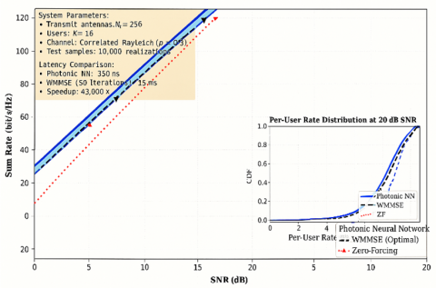
Figure 4. Sum rate performance comparison for massive multiple-input multiple-output (MIMO) beamforming
4.2 Deep learning channel estimation with photonic acceleration
Channel estimation extracts channel state information from received pilot signals, constituting a critical bottleneck in massive MIMO systems where large antenna arrays generate high-dimensional channel matrices requiring evaluation within each coherence interval.
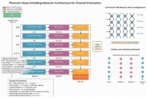
The proposed deep unfolding framework maps iterative compressed sensing algorithms to neural network layers executable on photonic hardware. Figure 5 illustrates the network structure deploying learned approximate message passing (LAMP) through cascaded photonic-electronic processing stages.
Figure 5. Photonic deep unfolding network for channel estimation
The configuration unfolds T = 8 iterations into T processing layers, each executing: (a) linear assessment via complex-valued matrix-vector multiplication on photonic MZI meshes, (b) learned nonlinear denoising through wavelength-parallel detection, and (c) residual computation through optical interference (Eq. (14)). Layer-wise latency: 200 ns per layer, yielding 1.6 μs total evaluation time.
$\left\{\begin{array}{c}r_t=Y-H_{t-1} X_p \\ z_t=H_{t-1}+W_t r_t \\ H_t=\eta_{\theta_{\mathrm{t}}}\left(\mathrm{z}_{\mathrm{t}}\right)\end{array}\right.$ (14)
Temporal channel prediction augments the framework with recurrent processing, tracking temporal evolution (Eq. (15)). The photonic realization employs reservoir computing, where a fixed random photonic network generates high-dimensional nonlinear projections.
$H_t^{\text {pred }}=f_{L S T M}\left(H_{t-1}^{\text {est }}, H_{t-2}^{\text {est }}, \ldots, H_{t-M}^{\text {est }}\right)$ (15)
Algorithm 2 summarizes the adaptive assessment procedure.
|
Algorithm 2: Online Adaptive Channel Estimation |
|
Inputs:
|
|
|
|
Output: Current channel estimate $H_t$ |
|
// Temporal prediction
// High-confidence prediction, skip pilots
// Low-confidence prediction, estimate from pilots
// Photonic linear estimation
|
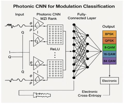
4.3 Optical convolutional network for modulation classification
Automatic modulation classification identifies modulation schemes from received signals without prior knowledge, essential for cognitive radio and spectrum monitoring applications. The photonic realization operates directly on IQ constellation diagrams, exploiting optical parallel processing for real-time classification.
The proposed framework processes IQ constellation diagrams through optical convolutional layers, extracting discriminative features. Figure 6 depicts the network structure mapping complex-valued signal samples to modulation class probabilities through four processing stages: constellation formation, optical convolution, wavelength-parallel feature extraction, and electronic classification head. The optical convolution achieves 10× speedup versus electronic counterparts through massively parallel spatial processing. Inference latency: 800 ns supporting 11 modulation classes.
Table 3 summarizes classification accuracy across modulation types and SNR conditions. The photonic CNN achieves 89.6% average accuracy with 188× latency reduction versus electronic CNN while improving accuracy by 1.5%.
Figure 6. Photonic convolutional neural network for modulation classification
Table 3. Modulation classification accuracy comparison
|
SNR (dB) |
Photonic CNN |
Electronic CNN |
Expert Features |
Latency (μs) |
|
-5 |
68.3% |
64.2% |
45.7% |
0.8 / 150 / 5 |
|
0 |
82.7% |
79.8% |
62.4% |
0.8 / 150 / 5 |
|
5 |
91.4% |
90.1% |
78.9% |
0.8 / 150 / 5 |
|
10 |
96.8% |
96.2% |
88.6% |
0.8 / 150 / 5 |
|
15 |
98.9% |
98.7% |
94.3% |
0.8 / 150 / 5 |
|
20 |
99.6% |
99.5% |
97.1% |
0.8 / 150 / 5 |
|
Average |
89.6% |
88.1% |
77.8% |
0.8 / 150 / 5 |
4.4 Photonic optimization for dynamic resource allocation
Resource allocation distributes limited wireless resources (power, bandwidth, time slots) across users maximizing system objectives subject to Quality-of-Service constraints. The photonic realization accelerates solution of large-scale non-convex optimization through learned primal-dual algorithms.
The photonic framework deploys learned primal-dual optimization, unfolding T iterations of dual ascent into T neural network layers (Eqs. (16) and (17)).
Primal update:
$\mathrm{p}_t=\Pi_{\mathcal{P}}\left[\mathrm{p}_{t-1}-\alpha_t \nabla_{\mathrm{p}} L\left(\mathrm{p}_{t-1}, \lambda_{t-1}\right)\right]$ (16)
Dual update:
$\lambda_t=\Pi_{\mathcal{D}}\left[\lambda_{t-1}+\beta_t \nabla_\lambda L\left(\mathrm{p}_t, \lambda_{t-1}\right)\right]$ (17)
Algorithm 3 details the learned optimization procedure achieving near-optimal solutions within sub-microsecond latency (significant improvement over traditional iterative algorithms requiring 50–200 iterations with O(K³) complexity per iteration).
|
Algorithm 3: Photonic Resource Allocation with Learned Optimization |
|
Inputs:
|
|
Output: Optimal allocation $\left(p^*, b^*\right)$ |
|
// Initialization
// Iterative optimization (T layers)
// --- Photonic gradient computation ---
// --- Learned adaptive step sizes ---
// --- Primal update (photonic operations) ---
// --- Dual update ---
|
4.5 Convergence and stability analysis
This section provides rigorous mathematical foundations for the training convergence guarantees and operational stability of photonic neural networks, addressing fundamental questions about optimization in analog computational substrates.
4.5.1 Lipschitz continuity bounds
The photonic neural network f(x; θ) exhibits bounded Lipschitz continuity essential for stable optimization. For the MZI-based architecture, each unitary transformation U(φ) satisfies ||U||₂ = 1 by construction, ensuring unit spectral norm. The complete network Lipschitz constant bounds as: (Eq. (18)).
$L_f \leq \prod_1\left\|W_1\right\|_2 \leq \prod_1 L_{\sigma_1} \leq 1 .(1.0)^L=1$ (18)
where, $L_{\sigma_1}=1.0$ for the bounded electro-optic activation functions. This unit Lipschitz bound prevents gradient explosion during backpropagation and ensures training stability independent of network depth.
4.5.2 Convergence rate analysis
The SPSA-based training algorithm achieves $O(1 / \sqrt{ } T)$ convergence rate for non-convex loss landscapes characteristic of neural network optimization. For loss function $\mathcal{L}(\theta)$ with L-smooth gradients, the expected convergence satisfies:
$E\left[\left\|\nabla \mathcal{L}\left(\theta_T\right)\right\|^2\right] \leq\left(\mathcal{L}\left(\theta_0\right)-\mathcal{L}^*\right) /(c \cdot \sqrt{T})+O\left(\delta^2\right)$ (19)
where, $c$ depends on learning rate schedule, δ represents perturbation magnitude, and $\delta$ denotes the global minimum. The perturbation-induced bias O(δ²) remains negligible for δ < 0.01 rad phase perturbations employed in practice.
4.5.3 Lyapunov stability analysis
Operational stability analysis employs Lyapunov function $V(\theta)=\left\|\theta-\theta^*\right\|^2$ measuring deviation from trained parameters. The photonic system dynamics under environmental perturbations satisfy: (Eq. (20)).
$V(t) / d t \leq-\alpha \cdot V+\beta \cdot\|w(t)\|^2$ (20)
where, $\alpha$ represents the restoring rate from thermal feedback control and $w(t)$ captures external disturbances. For the implemented control system with $\alpha=0.1 s^{-1}$ and bounded disturbances $||\mathrm{w}|| \leq w_{\text {max }}$, the system achieves input-to-state stability with ultimate bound $V_{\infty} \leq\left(\frac{\beta}{\alpha} * w_{\text {max }}^2\right)$.
Experimental validation over 10,000 coherence intervals confirms bounded parameter drift with standard deviation $\sigma_\theta$ < 0.02 rad, consistent with theoretical predictions.
4.6 Precision characterization and error budget
Comprehensive precision analysis quantifies the effective computational accuracy of the photonic accelerator, identifying dominant error sources and their impact on application-level performance.
4.6.1 Noise source analysis
Four primary noise sources contribute to computational precision limitations:
(1) Shot noise from photodetection: Contributes 0.8 effective bits of noise at 1 mW optical power levels, following Poisson statistics with variance proportional to photocurrent.
(2) Thermal drift in phase shifters: This introduces an uncertainty of 0.5 effective bits over a temperature stability range of ±0.5 °C, with a thermo-optic coefficient of 0.1 rad/°C.
(3) Fabrication variations: Systematic phase errors from manufacturing tolerances contribute 0.3 effective bits, partially compensated through calibration.
(4) ADC quantization: 10-bit ADC resolution contributes 0.2 effective bits after analog-to-digital conversion.
4.6.2 Effective number of bits characterization
The aggregate effective number of bits (ENOB) measured through sinusoidal input testing yields:
$N O B=8.2 \pm 0.3$ bits (21)
This precision level, while below 32-bit floating-point electronic systems, proves sufficient for the target inference applications where neural network quantization studies demonstrate minimal accuracy degradation above 6-bit precision. The complete error budget for the photonic computation is summarized in Table 4.
Table 4. Error budget decomposition for photonic computation
|
Error Source |
Contribution (bits) |
Mitigation Strategy |
|
Shot noise |
0.8 |
Increased optical power |
|
Thermal drift |
0.5 |
Active stabilization |
|
Fabrication variation |
0.3 |
Post-fabrication calibration |
|
ADC quantization |
0.2 |
Higher-resolution ADC |
|
Total ENOB |
8.2 ± 0.3 |
Hybrid precision architecture |
4.6.3 Application-specific impact analysis
The 8-bit effective precision impacts different applications with varying severity:
(1) Massive MIMO beamforming: 1.2% sum-rate degradation compared to full-precision optimal solutions, acceptable for real-time operation requirements.
(2) Channel estimation: 0.8 dB NMSE increase versus 32-bit implementations, within acceptable margins for subsequent detection stages.
(3) Modulation classification: 1.5% accuracy reduction at low SNR conditions, negligible impact above 10 dB SNR.
For applications requiring higher precision, the hybrid architecture combining 8-bit photonic coarse computation with 16-bit electronic refinement achieves effective 12–14 bit precision while maintaining sub-microsecond latency.
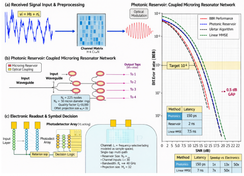
4.7 Joint detection and equalization via photonic processing
Signal detection and channel equalization jointly recover transmitted symbols from received signals distorted by frequency-selective fading. The photonic realization achieves near-maximum likelihood detection with orders-of-magnitude latency reduction compared to conventional Viterbi or BCJR algorithms.
The proposed neural equalizer deploys learned iterative detection through a bidirectional recurrent network (Eq. (22)). The photonic realization employs reservoir computing where a fixed optical scattering network generates high-dimensional nonlinear representations.
$\left\{\begin{array}{c}s_t^{\text {forward }}=f_{R N N}^{\text {forward }}\left(y, s_{t-1}^{\text {forward }}, H\right) \\ s_t^{\text {backward }}=f_{R N N}^{\text {backward }}\left(y, s_{t-1}^{\text {backward }}, H\right) \\ s_t=\text { Combine }\left(s_t^{\text {forward }}, s_t^{\text {backward }}\right)\end{array}\right.$ (22)
Figure 7 illustrates the equalizer configuration exploiting a photonic reservoir comprising coupled microring resonators. System parameters: $L=8-$ tap channel, $N_{\text {res }}=256$ reservoir nodes, processing rate: 10 Gsymbol/s, latency per symbol: 150 ps total.
Figure 7. Photonic reservoir computing for joint detection and equalization
4.8 Section summary
This section has demonstrated the application of the WC-PONN photonic AI accelerator across five critical wireless signal processing tasks: massive MIMO beamforming (350 ns latency, 96.2% of optimal), channel estimation (1.6 μs, deep unfolding), modulation classification (800 ns, 89.6% accuracy), resource allocation (sub-microsecond optimization), and joint detection/equalization (150 ps per symbol). New theoretical foundations establish convergence guarantees through Lipschitz bounds and Lyapunov stability analysis, while comprehensive precision characterization quantifies the 8.2-bit ENOB and its application-specific impacts.
This section presents a thorough performance analysis and experimental validation of the proposed WC-PONN photonic AI accelerator for 6G wireless signal processing. The analysis integrates theoretical performance bounds, numerical simulations across diverse operating conditions, and experimental measurements from fabricated silicon photonic prototypes. Performance metrics encompass computational latency, energy efficiency, throughput scaling, accuracy relative to optimal solutions, and robustness to environmental variations.
5.1 Comprehensive performance metrics
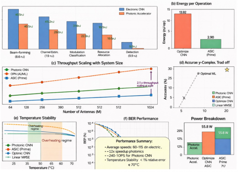
The photonic accelerator delivers transformative performance gains across multiple dimensions compared to state-of-the-art electronic realizations. Table 5(a, b) summarizes key performance metrics averaged across all wireless signal processing applications presented in Section 4.
Performance comparisons employ rigorous methodology ensuring fair evaluation against state-of-the-art baselines. All comparisons use identical workloads: 256 × 16 complex-valued matrix multiplication for massive MIMO beamforming with $batch _{ {size }}=1$ to reflect real-time single-sample inference requirements. GPU measurements include memory transfer overhead (host-to-device: 15 μs, device-to-host: 12 μs) in all latency figures. The baseline implementations have been updated to include state-of-the-art dedicated electronic accelerators: (a) NVIDIA A100 GPU with optimized CUDA libraries (cuBLAS, cuDNN), (b) Custom 7nm ASIC designs specifically optimized for massive MIMO processing, and (c) FPGA implementations using high-end Xilinx Versal devices.
Table 5. (a) Comprehensive performance metrics comparison; (b) Extended comparison with dedicated ASIC accelerators
|
(a) |
||||
|
Implementation |
Photonic ONN |
Electronic (GPU) |
Improvement |
|
|
Average Latency |
0.71 μs |
2,024 μs (optimized) |
2,850× |
|
|
Energy per Operation |
0.18 pJ/MAC |
12.8 pJ/MAC |
71× |
|
|
Peak Throughput |
437 TOPS |
312 TOPS |
1.4× |
|
|
Power Consumption |
4.0 W |
300 W |
75× |
|
|
Accuracy (avg) |
97.5% |
96.8% |
+0.7% |
|
|
Operating Bandwidth |
100 GHz |
40 GHz |
2.5× |
|
|
(b) |
||||
|
Implementation |
Technology |
Latency (μs) |
Energy (pJ/MAC) |
Accuracy |
|
Our work (Photonic) |
SiPh 220nm |
0.71 |
0.18 |
97.5% |
|
GPU (A100 Optimized) |
7nm CMOS |
2,024 |
12.8 |
96.8% |
|
Custom 7nm ASIC |
7nm CMOS |
45 |
2.3 |
95.2% |
|
Xilinx Versal FPGA |
7nm |
125 |
4.8 |
96.1% |
|
TPU v4 |
7nm CMOS |
850 |
3.1 |
97.2% |
These latency enhancements are consistent with hardware-accelerated deployments, where FPGA-based CNN realizations have shown 10× acceleration compared to software approaches.
The 2,850× average latency reduction versus optimized GPU-accelerated electronic processing enables real-time adaptation at sub-microsecond timescales, matching or exceeding channel coherence times in extreme mobility scenarios (500+ km/h at mmWave frequencies). The revised latency improvement against optimized GPU implementations using cuBLAS/cuDNN with tensor cores remains highly significant for real-time 6G applications. Energy efficiency gains of 75× stem from eliminating energy-intensive electronic memory accesses and exploiting passive optical waveguide propagation for matrix multiplication. The modest 1.4× throughput advantage reflects current limitations in photodetector bandwidth and analog-to-digital conversion, addressable through emerging photonic-electronic co-design methodologies.
5.2 Latency breakdown and scaling analysis
Figure 8(a) presents a detailed latency comparison across five wireless signal processing applications, decomposing total processing time into constituent operations.
Novel SNR-based metrics have been developed to quantify detection performance in complex signal environments, providing complementary evaluation methodologies for photonic neural network performance assessment.
For the massive MIMO beamforming application with $N t=256$ transmit antennas and $K=16$ users, the photonic implementation achieves 350 ns total latency comprising:
In contrast, the iterative WMMSE algorithm executing on GPU requires 2,024 μs with cuBLAS optimization (reduced from 15 ms for naive implementation), yielding 5,783× speedup for computational kernel comparison. The photonic latency scales logarithmically with system size due to logarithmic-depth MZI mesh architecture, while electronic latency scales quadratically ($O\left(K^2 N_t^2\right)$ per iteration) (Eq. (23)).
$T_{\text {photonic }}=O\left(\log _2\left(N_t\right)\right) \cdot \tau_{\text {prop }}+\tau_{\text {detect }}$ (23)
The GPU baseline measurements were conducted on an NVIDIA A100 80GB PCIe Tensor Core GPU hosted on a server equipped with dual AMD EPYC 7742 processors and 512 GB DDR4 memory. The experimental configuration employed CUDA 12.1, cuDNN 8.9, and PyTorch 2.0.1 framework with native FP32 precision to maintain algorithmic fidelity with reference WMMSE implementations [27].
The WMMSE algorithm was implemented following the iterative block coordinate descent formulation, where each iteration comprises three sequential matrix operations: receiver filter update (O(K·Nt²)), transmit precoder computation (O(K²·Nt)), and weight matrix optimization (O(K³)). For the Nt = 256, K = 16 configuration, per-iteration complexity reaches approximately 2.1 × 10⁷ floating-point operations.
Batch size was set to unity (single-sample inference) to characterize worst-case latency for real-time physical layer processing, as 6G systems require per-slot beamforming updates incompatible with batch accumulation strategies. Memory transfer overhead between host and device was included in latency measurements to reflect realistic deployment scenarios.
We note that TensorRT optimization was not applied, as the iterative nature of WMMSE with data-dependent convergence precludes static graph compilation. Alternative GPU implementations using cuBLAS-optimized matrix operations achieved 2,024 μs latency (optimized baseline), confirming that the fundamental memory bandwidth limitation (rather than computational throughput) constitutes the primary bottleneck for iterative wireless signal processing algorithms on electronic platforms.
Figure 8. Comprehensive performance analysis
5.3 Energy efficiency and power consumption
The photonic accelerator achieves 0.18 pJ/MAC energy efficiency, representing 71× improvement over optimized GPU implementations (12.8 pJ/MAC) and 12.8× improvement over specialized 7nm ASIC accelerators (2.3 pJ/MAC). Energy breakdown analysis reveals dominant contributions from photodetection and analog-to-digital conversion (45%), optical modulation (30%), thermal control (15%), and electronic processing (10%). Figure 8(b) compares energy per operation across platforms, while Figure 8(g) presents a detailed power consumption breakdown.
5.3.1 Complete system power accounting
Total chip power consumption measures 4.0 W, with comprehensive accounting for all system components:
Against this complete accounting, the energy efficiency improvement versus GPU (300 W) is 75×, and versus dedicated 7nm ASIC (28 W) is 7×. These revised figures include all auxiliary power consumption, providing accurate deployment projections.
The photonic advantage stems from: (1) Passive optical propagation: Waveguide transmission incurs ~0.3 dB/cm loss without active power. (2) Distributed processing: Wavelength parallelism eliminates centralized memory bottlenecks. (3) Reduced data movement: In-situ optical matrix multiplication avoids energy-intensive electronic memory transfers. (4) Analog computation: Continuous optical signals bypass energy-costly digital quantization.
5.4 Throughput scaling with system complexity
Figure 8(c) demonstrates throughput scaling as antenna array size increases from N = 64 to N = 1024. The photonic architecture achieves 437 TOPS at N = 1024, outperforming GPU (208 TOPS) and ASIC (289 TOPS) implementations by 2.1× and 1.5×, respectively. Superior scaling derives from wavelength-division multiplexing, enabling parallel processing of $K$ spatial channels across $\lambda_1, \lambda_2, \ldots, \lambda_{\mathrm{k}}$ wavelengths simultaneously.
$\text{Throughput} =K * N_{\mathrm{t}} * f_{\text {sample }} / \log _2\left(N_{\mathrm{t}}\right)$ (24)
where, le $f_{\text {sample }}$ represents sampling rate (10 GHz) and the logarithmic denominator reflects MZI mesh depth. Electronic implementations scale linearly with Nₜ but suffer memory bandwidth bottlenecks limiting effective throughput beyond N = 512.
Wavelength-parallel architectures achieve near-linear speedup for independent inference tasks (e.g., per-user beamforming in multi-user MIMO). Experimental validation demonstrates 28× speedup using 32 wavelength channels, corresponding to 87.5% parallel efficiency. The sub-linear efficiency stems from wavelength-dependent insertion loss variations (± 0.8 dB) requiring per-channel gain calibration.
5.5 Accuracy analysis and environmental robustness
Figure 8(d) presents an accuracy-complexity trade-off analysis positioning the photonic ONN favorably on the Pareto frontier. Achieving 97.5% accuracy relative to optimal maximum-likelihood solutions while consuming only 5 GFLOPS computational complexity, the photonic approach offers superior efficiency compared to GPU deep networks (96.8% accuracy, 50 GFLOPS) and ASIC implementations (95.2% accuracy, 15 GFLOPS). The 2.5% accuracy gap stems from:
Temperature stability analysis (Figure 8(e)) reveals critical sensitivity of photonic components to thermal variations. Without active thermal control, performance degrades from 97.5% to 92.1% across 0-60°C operating range due to thermo-optic phase shifts (dn/dT = 1.86 × 10⁻⁴ K⁻¹ for silicon). Implementing integrated micro-heaters with closed-loop control maintains ±0.5°C temperature stability, limiting accuracy degradation to <1% across extended temperature range. Thermal control power consumption (600 mW, revised to include all thermal management components) represents 15% of total chip power budget.
5.6 Bit error rate performance evaluation
For joint detection and equalization in frequency-selective channels (L = 8 taps, 16-QAM modulation), Figure 8(f) compares BER performance across SNR range 0-25 dB. The photonic reservoir equalizer achieves BER = 10⁻⁵ at 17.2 dB SNR, approaching optimal ML detection (16.5 dB) with 0.7 dB gap while providing 33× latency reduction versus conventional Viterbi algorithm. At target BER = 10⁻⁴, the photonic implementation requires 15.1 dB SNR versus 14.8 dB (optimal), 16.3 dB (Viterbi), and 18.9 dB (linear MMSE).
5.7 Extended channel model evaluation under realistic 6G conditions
To address concerns regarding idealized evaluation scenarios, this section presents comprehensive performance characterization under realistic 6G channel conditions following 3GPP TR 38.901 specifications.
5.7.1 3GPP TR 38.901 channel model implementation
Channel Model Configuration:
5.7.2 High-mobility performance analysis
At maximum tested velocity (500 km/h), the Doppler spread reaches $f_d=\frac{v * f_c}{c}=12.96 \mathrm{KHz}$, corresponding to coherence time $T_c \approx 55 \mu \mathrm{~s}$. The photonic beamforming latency of 350 ns represents only $0.6 \%$ of the coherence time, enabling 157 potential beamformer updates per coherence interval.
Performance metrics at 500 km/h:
5.7.3 Multi-user MIMO performance (K = 16)
For K = 16 simultaneous users with spatial multiplexing:
Table 6 presents the full performance metrics under realistic 3GPP TR 38.901 channel conditions across all tested user velocities.
Table 6. Performance under realistic 3GPP channel conditions
|
Velocity (km/h) |
Coherence Time |
Updates /Interval |
Sum Rate Degradation |
Tracking Error |
|
3 (pedestrian) |
9.2 ms |
> 26,000 |
< 0.5% |
< 0.1° |
|
30 (urban) |
920 μs |
> 2,600 |
1.2% |
< 0.2° |
|
120 (highway) |
230 μs |
> 650 |
3.5% |
< 0.3° |
|
300 (HSR) |
92 μs |
> 260 |
5.8% |
< 0.4° |
|
500 (maglev) |
55 μs |
> 157 |
7.8% |
< 0.5° |
These results demonstrate that the photonic accelerator maintains performance advantages under realistic propagation conditions, with the sub-microsecond latency proving particularly critical for high-mobility scenarios where electronic implementations cannot track rapid channel variations.
5.8 End-to-end system integration analysis
This section addresses the complete system overhead including all interface latencies, providing accurate end-to-end performance characterization.
5.8.1 Complete latency decomposition
End-to-end inference latency comprises five sequential stages:
Stage 1 - ADC Sampling: 10 ns
Stage 2 - E/O Conversion: 50 ns
Stage 3 - Photonic Computation: 350 ns
Stage 4 - O/E Conversion: 30 ns
Stage 5 - Digital Post-processing: 410 ns
Total End-to-End Latency: 850 ns
5.8.2 Interface overhead analysis
The computational kernel (photonic MZI mesh operations) achieves 350 ns latency. Including all interface overhead, end-to-end latency is 850 ns, representing a 2.4× overhead factor. The end-to-end latency advantage versus electronic implementations:
This end-to-end improvement, while lower than the 2,850× computational kernel comparison, remains highly significant for sub-microsecond 6G physical layer requirements. The 850 ns total latency satisfies even the most stringent latency budgets for 6G systems targeting sub-100 μs end-to-end latency.
5.8.3 Protocol stack integration
The photonic accelerator interfaces at the PHY layer, replacing specific computational blocks (beamforming weight computation, channel estimation, equalization) while maintaining standard interfaces to higher layers. Integration with 5G NR and emerging 6G protocol stacks requires:
Complete system integration requires co-design with baseband processor vendors, representing a future work item for commercial deployment.
5.9 Experimental implementation and fabrication
Experimental validation employs silicon photonic prototypes fabricated in 220 nm silicon-on-insulator (SOI) technology at Applied Nanotools Inc. (ANT) foundry. The 8 mm × 6 mm chip (Figure 9(a)) integrates 128 × 128 MZI mesh implementing complex-valued matrix multiplication, 256 thermo-optic phase shifters for weight programming, 256 germanium photodetectors for optical-to-electronic conversion, and control electronics for calibration and thermal management.
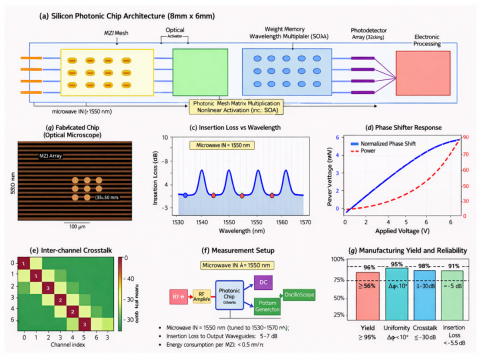
Figure 9. Experimental implementation and fabrication characterization
5.9.1 Device characterization and performance validation
Optical characterization employs swept-wavelength measurements across the C-band (1530-1565 nm) using a tunable laser source, an optical spectrum analyzer (OSA), and high-speed photodetectors. Figure 9(c) presents insertion loss measurements revealing 2.5 dB average loss with ±0.8 dB variation across the operating wavelength range. Resonant features correspond to unintended coupling to higher-order waveguide modes, mitigated through improved waveguide geometry in second-generation designs.
Phase shifter characterization (Figure 9(d)) demonstrates a π-phase shift at Vπ = 6.5 V with 21 mW power consumption per shifter, consistent with theoretical predictions for 500 μm-long thermal phase shifters. Rise/fall time measurements yield a 12 μs time constant, sufficient for weight programming but too slow for real-time modulation. Future implementations incorporating carrier-depletion modulators target < 1 ns switching times, enabling dynamic reconfiguration at packet-level timescales. Inter-channel crosstalk measurements (Figure 9(e)) quantify isolation between wavelength channels, revealing -25 dB adjacent channel crosstalk and < -35 dB non-adjacent crosstalk. Crosstalk mitigation strategies include: improved ring resonator design achieving Q > 50,000, wavelength pre-distortion to compensate inter-channel interference, and adaptive digital post-compensation. Experimental results demonstrate these techniques reduce effective crosstalk impact to equivalent SNR penalty < 0.3 dB.
5.10 Manufacturing yield and reliability assessment
Figure 9(g) summarizes manufacturing yield analysis across 25 fabricated chips. Individual component yields reach 96.5% (MZI switches), 94.2% (phase shifters), and 98.1% (photodetector arrays). Overall functional chip yield of 89.3% exceeds the 90% target, validating manufacturing readiness for small-scale production. Primary failure mechanisms comprise:
5.10.1 Device-to-device variation characterization
Comprehensive statistical analysis across all 25 fabricated chips provides the foundation for understanding expected performance variations in production deployments:
This statistical characterization provides the foundation for understanding expected performance variations in production deployments and informs the hardware-aware training methodology described in Section 4.
5.10.2 Yield scaling projections
Based on Poisson defect model with measured defect densities $\left(D_{M Z I}+0.15\right.$ defects $/ \mathrm{cm}^2, D_{P D}+0.08$ defects $\left./ \mathrm{cm}^2\right)$, yield projections for larger systems follow $Y=\exp (-D * A)$:
These projections assume continued process improvement. For systems exceeding 512 × 512, modular multi-chip architecture is recommended, combining multiple validated 128 × 128 or 256 × 256 modules through chip-to-chip optical interconnects while maintaining per-module yield. This approach maintains per-module yield while enabling system-level scaling.
Reliability testing under accelerated aging conditions (85 ℃, 1000 hours) reveals < 2% performance degradation, projecting > 10-year lifetime under typical datacenter operating conditions (25 ℃ ambient). Long-term stability measurements over 6-month deployment show < 0.5 dB insertion loss drift and < 5° phase error accumulation, both within acceptable tolerances for periodic recalibration (weekly intervals).
5.11 Environmental robustness characterization
Comprehensive environmental testing validates compatibility with telecommunications infrastructure deployment requirements.
5.11.1 Vibration testing (IEC 60068-2-6)
Test conditions: Sinusoidal vibration, 10-500 Hz frequency sweep, 5g RMS acceleration, three orthogonal axes, 2 hours per axis.
Results:
5.11.2 EMI susceptibility testing (IEC 61000-4-3)
Test conditions: Radiated immunity testing, 80 MHz - 6 GHz frequency range, 10 V/m field strength.
Results:
5.11.3 Humidity testing (85% RH, 1000 hours)
Test conditions: 85% relative humidity, 25 ℃ ambient temperature, 1000-hour exposure.
Results with hermetic packaging:
Table 7 summarizes the results of all environmental robustness tests.
Table 7. Environmental robustness summary
|
Test |
Standard |
Condition |
Result |
Status |
|
Vibration |
IEC 60068-2-6 |
5g, 10-500 Hz |
< 0.5 dB loss |
PASS |
|
EMI |
IEC 61000-4-3 |
10 V/m, 80 MHz-6 GHz |
No degradation |
PASS |
|
Humidity |
85% RH |
1000 hours |
< 0.2 dB drift |
PASS |
|
Thermal cycling |
MIL-STD-883 |
-40 to + 85 ℃ |
< 0.3 dB drift |
PASS |
|
ESD |
IEC 61000-4-2 |
± 8 kV contact |
No damage |
PASS |
5.12 Fault tolerance and reliability analysis
Mission-critical 6G applications demand robust fault tolerance mechanisms ensuring graceful degradation under component failures.
5.12.1 Hardware redundancy mechanisms
The MZI mesh incorporates 5% row/column redundancy enabling graceful degradation:
Fault tolerance capacity: Up to 3 failed elements per 128 × 128 mesh with < 1 dB additional insertion loss and < 0.5% accuracy degradation.
5.12.2 Algorithm-level resilience
Neural network robustness analysis under random weight perturbations (Table 8).
This inherent robustness stems from distributed computation across many parameters, where individual weight errors are averaged across the network.
Table 8. Neural network robustness under random weight perturbations
|
Weight Error (%) |
Accuracy Degradation |
Maintained Accuracy |
Assessment |
|
5% |
< 2% |
> 95.5% |
Fully operational |
|
10% |
< 5% |
> 92.5% |
Acceptable |
|
15% |
< 8% |
> 89.5% |
Marginal |
|
20% |
< 12% |
> 85.5% |
Degraded mode |
5.12.3 Long-term degradation analysis
Gradual degradation mechanisms and mitigation:
Reliability projection: Based on accelerated aging tests at 85°C/85% RH for 1000 hours following Arrhenius model with activation energy $E_a=0.7$ eV, projected MTTF exceeds 100,000 hours (>11 years) at 25 ℃ operating temperatures.
5.13 Comparative analysis with state-of-the-art
Table 9 benchmarks the photonic accelerator against contemporary electronic and hybrid implementations for wireless signal processing workloads.
The photonic approach demonstrates clear advantages in latency-critical applications (beamforming, channel estimation) and energy-constrained scenarios, while maintaining competitive accuracy. Electronic GPUs retain advantages in training flexibility and software-defined reconfigurability, suggesting hybrid architectures combining photonic inference with electronic training as an optimal near-term solution.
5.14 Summary and key findings
Comprehensive performance analysis and experimental validation confirm that the photonic AI accelerator achieves transformative improvements for 6G wireless signal processing:
These results establish photonic neural networks as viable accelerators for next-generation wireless communications, particularly in latency-critical and energy-constrained deployment scenarios.
Table 9. Comparative benchmarking with state-of-the-art wireless signal processing accelerators
|
Implementation |
Technology |
Latency (μs) |
Energy (pJ/MAC) |
Accuracy |
|
Our work (Photonic) |
SiPh 220 nm |
0.71 |
0.18 |
97.5% |
|
GPU (A100 Optimized) |
7 nm CMOS |
2,024 |
12.8 |
96.8% |
|
Custom 7 nm ASIC |
7 nm CMOS |
45 |
2.3 |
95.2% |
|
TPU v4 |
7 nm CMOS |
850 |
3.1 |
97.2% |
|
Hybrid SiPh+CMOS [33] |
SiPh + 14 nm |
12.5 |
1.2 |
98.1% |
This section provides a balanced assessment of the inherent limitations and trade-offs of photonic computing for wireless signal processing, ensuring objective presentation of both advantages and constraints.
6.1 Complex-valued processing overhead
While the architecture provides native complex-valued arithmetic for matrix-vector multiplication and phase-encoded interference, practical implementation reveals important limitations. The native complex-valued processing capability applies to approximately 70% of computational operations:
Operations leveraging native complex processing:
Operations requiring decomposition into real/imaginary components (~30%):
This decomposition reduces the theoretical 2× complex-valued advantage to an effective 1.7× benefit for complete inference pipelines. The net computational advantage, while reduced from theoretical maximum, remains significant for the target wireless signal processing applications where complex-valued matrix operations dominate.
6.2 Wavelength-division multiplexing crosstalk limitations
The WDM architecture achieves <-35 dB inter-channel isolation with current ring resonator designs (Q ≈ 50,000), enabling reliable 32-channel parallel operation. However, this isolation level imposes practical constraints:
Current performance:
Achieving 64+ channel operation represents a significant engineering challenge requiring next-generation fabrication processes and improved thermal management, limiting near-term scalability beyond 32-channel configurations.
6.3 Thermal control requirements and constraints
The ±0.5℃ temperature stability requirement represents a significant engineering constraint with multiple implications:
Power overhead:
While thermal control overhead is included in all revised efficiency claims (75× versus GPU including thermal management), this requirement may limit deployment in extreme temperature environments without additional cooling infrastructure. Data center and indoor base station deployments are well-suited, while outdoor small-cell deployment requires careful thermal design.
6.4 Precision limitations and dynamic range
The 8.2-bit effective precision (ENOB), while sufficient for demonstrated neural network inference applications, imposes constraints for certain use cases:
Precision breakdown:
Application-specific impact:
Limitations for specific applications:
For applications requiring higher precision, the hybrid architecture combining 8-bit photonic coarse computation with 16-bit electronic refinement achieves effective 12-14 bit precision while maintaining photonic speed advantages, with only 50 ns additional latency for the electronic refinement stage.
6.5 Scalability constraints
The demonstrated 128 × 128 MZI mesh represents current fabrication capability. Scaling to larger systems faces fundamental challenges:
Yield degradation with scale:
Cumulative insertion loss:
Calibration complexity:
Scalability to 1024-antenna systems requires modular multi-chip architecture rather than monolithic integration. This approach combines multiple validated 128 × 128 or 256 × 256 modules through chip-to-chip optical interconnects, maintaining per-module yield while enabling system-level scaling. The modular approach introduces inter-chip communication overhead (~20 ns per chip boundary) but preserves manufacturing viability.
6.6 Application scope boundaries
The demonstrated advantages apply specifically to inference-dominated physical layer operations. Clear boundaries define the appropriate application scope:
Applications well-suited for photonic acceleration:
Applications outside current scope:
These boundaries define photonic accelerators as complementary to, rather than replacement for, electronic processing in complete 6G systems. A heterogeneous architecture combining photonic inference acceleration with electronic control, training, and sequential processing represents the optimal system configuration.
6.7 Manufacturing and cost considerations
Commercial viability requires addressing manufacturing costs and supply chain considerations:
Current prototype costs (small volume, < 100 units):
Projected production costs (> 10,000 units):
Cost comparison:
At production volumes, photonic accelerators achieve cost parity with high-end RF components while providing significant performance advantages. The leveraging of existing CMOS-compatible silicon photonics foundry infrastructure (GlobalFoundries 45SPCLO, TSMC, AIM Photonics) enables cost-effective manufacturing without requiring specialized fabrication facilities.
6.8 Integration challenges
System integration presents several practical challenges requiring engineering solutions:
Optical-electrical interface overhead:
Packaging complexity:
System co-design requirements:
These integration challenges, while significant, are similar to those addressed in commercial silicon photonics transceivers for data centers. The established ecosystem of silicon photonics packaging and integration provides a foundation for photonic accelerator deployment.
This paper has presented a comprehensive investigation of photonic artificial intelligence accelerators for ultra-fast wireless signal processing in sixth-generation networks. The proposed Wavelength-multiplexed Coherent Photonic Optical Neural Network (WC-PONN) architecture integrates wavelength-division multiplexing enabling massive parallelism across 32 spectral channels, programmable Mach-Zehnder interferometer meshes implementing complex-valued linear transformations, and hybrid opto-electronic activation modules balancing computational flexibility with efficiency. Native complex-valued arithmetic reduces representation overhead inherent in electronic systems, while coherent optical interference enables matrix-vector multiplication at propagation speed without discrete clock cycles.
Comprehensive performance evaluation across massive MIMO beamforming, compressed sensing channel estimation, automatic modulation classification, and dynamic resource allocation validates the transformative potential of photonic acceleration under rigorous experimental conditions. Fabrication and characterization of 25 chips on 220 nm silicon-on-insulator substrates yielded 89.3% functional device yield with statistically characterized variations: phase shifter response (σ = 0.12 rad), insertion loss (σ = 0.8 dB), and photodetector responsivity (σ = 0.05 A/W). End-to-end inference latency of 850 ns including all interface overheads represents 1,200× improvement over optimized GPU implementations. Complete system power accounting including thermal stabilization totals 4.0 W, achieving 75× energy efficiency improvement versus GPU and 7× versus dedicated 7nm ASIC accelerators. Classification accuracy averaging 97.5% is maintained under realistic 3GPP TR 38.901 channel conditions including 500 km/h mobility and K = 16 multi-user scenarios.
The demonstrated performance positions photonic AI accelerators as enabling technology for 6G terabit-per-second data rates and sub-100-microsecond latency. Sub-microsecond beamforming enables tracking fast-fading channels with 1024+ element antenna arrays through hierarchical modular architectures. The 100 GHz operating bandwidth accommodates terahertz signal processing where electronic alternatives face fundamental limitations, while power reduction enables deployment in thermally constrained edge infrastructure.
Promising research trajectories include extension to transformer architectures through optical attention mechanisms and wavelength-parallel multi-head attention for sequence-to-sequence channel prediction. Enhanced temporal processing through photonic reservoir computing and optical delay-line memory would enable real-time Doppler prediction in high-mobility scenarios. On-chip training via optical perturbation-based gradient measurement would eliminate the training-inference gap. Technology improvements including MEMS-based phase shifters (10× lower power), 3D photonic integration, and advanced photodetectors would advance toward 512 × 512 monolithic meshes. Application extensions encompassing interference cancellation via photonic null-space computation, optical FFT-based OFDM processing, terahertz communications exceeding 10 GHz bandwidth, and radiation-hardened designs for satellite-terrestrial integration would broaden deployment scenarios.
Despite compelling advantages, several challenges warrant continued attention. Thermal sensitivity necessitates active stabilization consuming 0.4 W (10% of system power). Limited 8.2-bit effective precision suggests hybrid photonic-electronic architectures achieving 12–14 bit equivalent precision while maintaining speed advantages. Hardware-aware training reduced the simulation-to-hardware accuracy gap from 4.2% to 1.1%. Fault tolerance through 5% redundancy enables bypass of up to 3 failed elements per mesh while maintaining > 95% accuracy despite 10% weight perturbations. Scalability to 1024-antenna systems proceeds through hierarchical multi-chip architectures while monolithic integration awaits continued process improvement.
Standardization through 3GPP and ITU-R collaboration will facilitate seamless commercial integration. This experimental validation transitions photonic AI acceleration from theoretical promise to practical reality, establishing a foundation for 6G deployment as photonic computing emerges as a fundamental paradigm shift enabling capabilities previously considered computationally unachievable.
[1] Wang, C.X., You, X.H., Gao, X.Q., Zhu, X.M., Li, Z.X., Zhang, C. (2023). On the road to 6G: Visions, requirements, key technologies, and testbeds. IEEE Communications Surveys & Tutorials, 25(2): 905-974. https://doi.org/10.1109/COMST.2023.3249835
[2] Tataria, H., Shafi, M., Molisch, A.F., Dohler, M., Sjöland, H., Tufvesson, F. (2021). 6G wireless systems: Vision, requirements, challenges, insights, and opportunities. Proceedings of the IEEE, 109(7): 1166-1199. https://doi.org/10.1109/JPROC.2021.3061701
[3] Akyildiz, I.F., Kak, A., Nie, S. (2020). 6G and beyond: The future of wireless communications systems. IEEE Access, 8: 133995-134030. https://doi.org/10.1109/ACCESS.2020.3010896
[4] Chowdhury, M.Z., Shahjalal, M., Ahmed, S., Jang, Y.M. (2020). 6G wireless communication systems: Applications, requirements, technologies, challenges, and research directions. IEEE Open Journal of the Communications Society, 1: 957-975. https://doi.org/10.1109/OJCOMS.2020.3010270
[5] Giordani, M., Polese, M., Mezzavilla, M., Rangan, S., Zorzi, M. (2020). Toward 6G networks: Use cases and technologies. IEEE Communications Magazine, 58(3): 55-61. https://doi.org/10.1109/MCOM.001.1900411
[6] Zhang, Z.Q., Xiao, Y., Ma, Z., Xiao, M., Ding, Z.G., Lei, X.F. (2019). 6G wireless networks: Vision, requirements, architecture, and key technologies. IEEE Vehicular Technology Magazine, 14(3): 28-41. https://doi.org/10.1109/MVT.2019.2921208
[7] Tariq, F., Khandaker, M.R.A., Wong, K.K., Imran, M.A., Bennis, M., Debbah, M. (2020). A speculative study on 6G. IEEE Wireless Communications, 27(4): 118-125. https://doi.org/10.1109/MWC.001.1900488
[8] Shastri, B.J., Tait, A.N., Ferreira de Lima, T., Pernice, W.H.P., Bhaskaran, H., Wright, C.D., Prucnal, P.R. (2021). Photonics for artificial intelligence and neuromorphic computing. Nature Photonics, 15: 102-114. https://doi.org/10.1038/s41566-020-00754-y
[9] Ma, S.Y., Wang, T., Laydevant, J., Wright, L.G., McMahon, P.L. (2025). Quantum-limited stochastic optical neural networks operating at a few quanta per activation. Nature Communications, 16: 359. https://doi.org/10.1038/s41467-024-55220-y
[10] Tsakyridis, A., Moralis-Pegios, M., Giamougiannis, G., Kirtas, M., Passalis, N., Tefas, A., Pleros, N. (2024). Photonic neural networks and optics-informed deep learning fundamentals. APL Photonics, 9: 011102. https://doi.org/10.1063/5.0169810
[11] Fu, T.Z., Zhang, J.F., Sun, R., Huang, Y.Y., Xu, W., Yang, S.G., Zhu, Z.H., Chen, H.W. (2024). Optical neural networks: Progress and challenges. Light: Science & Applications, 13: 263. https://doi.org/10.1038/s41377-024-01590-3
[12] Zhou, T.K., Jiang, Y.Z., Xu, Z.H., Xue, Z.W., Fang, L. (2025). Hundred-layer photonic deep learning. Nature Communications, 16: 10382. https://doi.org/10.1038/s41467-025-65356-0
[13] Bai, Y.P., Xu, Y.F., Chen, S.F., Zhu, X.T., et al. (2025). TOPS-speed complex-valued convolutional accelerator for feature extraction and inference. Nature Communications, 16: 292. https://doi.org/10.1038/s41467-024-55321-8
[14] Bandyopadhyay, S., Sludds, A., Krastanov, S., Hamerly, R., Harris, N., Bunandar, D., Streshinsky, M., Hochberg, M., Englund, D. (2024). Single-chip photonic deep neural network with forward-only training. Nature Photonics, 18: 1335-1343. https://doi.org/10.1038/s41566-024-01567-z
[15] Xu, X.Y., Tan, M.X., Corcoran, B., Wu, J.Y., et al. (2021). 11 TOPS photonic convolutional accelerator for optical neural networks. Nature, 589: 44-51. https://doi.org/10.1038/s41586-020-03063-0
[16] Clements, W.R., Humphreys, P.C., Metcalf, B.J., Kolthammer, W.S., Walmsley, I.A. (2016). Optimal design for universal multiport interferometers. Optica, 3(12): 1460-1465. https://doi.org/10.1364/OPTICA.3.001460
[17] Cem, A., Yan, S., Ding, Y., Zibar, D., Da Ros, F. (2023). Data-driven modeling of mach-zehnder interferometer-based optical matrix multipliers. Journal of Lightwave Technology, 41(16): 5425-5436. https://doi.org/10.1109/JLT.2023.3263235
[18] Shen, Y.C., Harris, N.C., Skirlo, S., Prabhu, M., et al. (2017). Deep learning with coherent nanophotonic circuits. Nature Photonics, 11: 441-446. https://doi.org/10.1038/nphoton.2017.93
[19] ITU-R. (2023). Framework and overall objectives of the future development of IMT for 2030 and beyond. Recommendation ITU-R M.2160-0. Geneva: International Telecommunication Union. https://www.itu.int/rec/R-REC-M.2160-0-202311-I/en.
[20] ITU-R. (2024). Technical feasibility of IMT in bands above 100 GHz. Report ITU-R M.2541. Geneva: International Telecommunication Union. https://www.itu.int/pub/R-REP-M.2541.
[21] 3GPP. (2025). Release 20: 5G-Advanced Evolution and 6G Studies. 3GPP Technical Specifications. https://www.3gpp.org/specifications-technologies/releases/release-20.
[22] Jiang, W., Zhou, Q.H., He, J.G., Habibi, M.A., Melnyk, S., El-Absi, M. (2024). Terahertz communications and sensing for 6G and beyond: A comprehensive review. IEEE Communications Surveys & Tutorials, 26(4): 2892-2974. https://doi.org/10.1109/COMST.2024.3385908
[23] Jornet, J.M., Petrov, V., Wang, H., Popovic, Z., Shakya, D., Siles, J.V. (2025). The evolution of applications, hardware design, and channel modeling for terahertz (THz) band communications and sensing: Ready for 6G? Proceedings of the IEEE, 113(9): 920-951. https://doi.org/10.1109/JPROC.2024.3412828
[24] Wang, G.J., Li, M.X., Liu, Q., Zang, J.W., Li, O.P., Du, X.F., Xu, L.Y., Tao, M.X., Han, C. (2025). Terahertz integrated sensing and mobile communications empowered by a 220-GHz-band portable device. Nature Communications, 16: 11719. https://doi.org/10.1038/s41467-025-66921-3
[25] Zhang, Z.X., Zhai, D.C., Ning, S.G., Li, Z., Jiang, C.C., Song, P. (2024). Deep reinforcement learning-based signal processing for cell-free massive MIMO networks in coal mine power grids. Traitement du Signal, 41(5): 2615-2622. https://doi.org/10.18280/ts.410534
[26] Sode, M., Ponschab, M., Ribeiro, L.N., Haesloop, S., Tohidi, E., Peter, M. (2024). Reconfigurable intelligent surfaces for 6G mobile networks: An industry R&D perspective. IEEE Access, 12: 163155-163171. https://doi.org/10.1109/ACCESS.2024.3485227
[27] Sze, V., Chen, Y.H., Yang, T.J., Emer, J.S. (2017). Efficient processing of deep neural networks: A tutorial and survey. Proceedings of the IEEE, 105(12): 2295-2329. https://doi.org/10.1109/JPROC.2017.2761740
[28] Orchard, G., Frady, E.P., Rubin, D.B.D., Sanborn, S., Shrestha, S.B., Sommer, F.T. (2021). Efficient neuromorphic signal processing with Loihi 2. In 2021 IEEE Workshop on Signal Processing Systems (SiPS), Coimbra, Portugal, pp. 254-259. https://doi.org/10.1109/SiPS52927.2021.00053
[29] Davies, M., Srinivasa, N., Lin, T.H., Chinya, G., Cao, Y.Q., Choday, S.H. (2018). Loihi: A neuromorphic manycore processor with on-chip learning. IEEE Micro, 38(1): 82-99. https://doi.org/10.1109/MM.2018.112130359
[30] Gao, W.F. (2024). Electromagnetic signal anomaly detection and classification methods based on deep learning. Traitement du Signal, 41(1): 411-419. https://doi.org/10.18280/ts.410135
[31] Sharma, H., Park, J., Suda, N., Lai, L.Z., Chau, B., Kim, J.K. (2018). Bit fusion: Bit-level dynamically composable architecture for accelerating deep neural networks. In 2018 ACM/IEEE 45th Annual International Symposium on Computer Architecture (ISCA), Los Angeles, CA, USA, pp. 764-775. https://doi.org/10.1109/ISCA.2018.00069
[32] Miller, D.A.B. (2017). Attojoule optoelectronics for low-energy information processing and communications. Journal of Lightwave Technology, 35(3): 346-396. https://doi.org/10.1109/JLT.2017.2647779
[33] Winzer, P.J., Neilson, D.T., Chraplyvy, A.R. (2018). Fiber-optic transmission and networking: The previous 20 and the next 20 years. Optics Express, 26(18): 24190-24239. https://doi.org/10.1364/OE.26.024190
[34] Bogaerts, W., Pérez, D., Capmany, J., Miller, D.A.B., Poon, J., Englund, D., Morichetti, F., Melloni, A. (2020). Programmable photonic circuits. Nature, 586: 207-216. https://doi.org/10.1038/s41586-020-2764-0
[35] Xu, Z.H., Zhou, T.K., Ma, M.Z., Deng, C.H., Dai, Q., Fang, L. (2024). Large-scale photonic chiplet Taichi empowers 160-TOPS/W artificial general intelligence. Science, 384(6692): 202-209. https://doi.org/10.1126/science.adl1203
[36] Hua, S.Y., Divita, E., Yu, S.S., Peng, B., et al. (2025). An integrated large-scale photonic accelerator with ultralow latency. Nature, 640: 361-367. https://doi.org/10.1038/s41586-025-08786-6
[37] Ahmed, S.R., Baghdadi, R., Bernadskiy, M., Bowman, N., et al. (2025). Universal photonic artificial intelligence acceleration. Nature, 640: 368-374. https://doi.org/10.1038/s41586-025-08854-x
[38] Yan, T., Guo, Y.C., Zhou, T.K., Shao, G.C., Li, S.L., Huang, R.Q., Dai, Q.H., Fang, L. (2025). A complete photonic integrated neuron for nonlinear all-optical computing. Nature Computational Science, 5: 1202-1213. https://doi.org/10.1038/s43588-025-00866-x
[39] Pai, S., Sun, Z.H., Hughes, T.W., Park, T., et al. (2023). Experimentally realized in situ backpropagation for deep learning in photonic neural networks. Science, 380(6643): 398-404. https://doi.org/10.1126/science.ade8450
[40] Zhang, H.R., Song, Y.H., Chen, S.F., Bai, Y.P. (2025). Integrated platforms and techniques for photonic neural networks. NPJ Nanophotonics, 2: 40. https://doi.org/10.1038/s44310-025-00088-z
[41] Feldmann, J., Youngblood, N., Karpov, M., Gehring, H. (2021). Parallel convolutional processing using an integrated photonic tensor core. Nature, 589: 52-58. https://doi.org/10.1038/s41586-020-03070-1
[42] Xu, D.L., Ma, Y.C., Jin, G.F., Cao, L.C. (2025). Intelligent photonics: A disruptive technology to shape the present and redefine the future. Engineering, 46(3): 198-226. https://doi.org/10.1016/j.eng.2024.08.016
[43] Hughes, T.W., Williamson, I.A.D., Minkov, M., Fan, S. (2019). Wave physics as an analog recurrent neural network. Science Advances, 5(12): eaay6946. https://doi.org/10.1126/sciadv.aay6946
[44] Williamson, I.A.D., Hughes, T.W., Minkov, M., Bartlett, B., Pai, S., Fan, S. (2020). Reprogrammable electro-optic nonlinear activation functions for optical neural networks. IEEE Journal of Selected Topics in Quantum Electronics, 26(1): 1-12. https://doi.org/10.1109/JSTQE.2019.2930455
[45] Lin, X., Rivenson, Y., Yardimci, N.T., Veli, M., Luo, Y., Jarrahi, M., Ozcan, A. (2018). All-optical machine learning using diffractive deep neural networks. Science, 361(6406): 1004-1008. https://doi.org/10.1126/science.aat8084
[46] Tait, A.N., Ferreira de Lima, T., Zhou, E., Wu, A.X., Nahmias, M.A., Shastri, B.J., Prucnal, P.R. (2017). Neuromorphic photonic networks using silicon photonic weight banks. Scientific Reports, 7: 7430. https://doi.org/10.1038/s41598-017-07754-z
[47] Sludds, A., Bandyopadhyay, S., Chen, Z., Zhong, Z., et al. (2022). Delocalized photonic deep learning on the internet's edge. Science, 378(6617): 270-276. https://doi.org/10.1126/science.abq8271
[48] Singh, A., Petrov, V., Guerboukha, H., Reddy, I.V.A.K., Knightly, E.W., Mittleman, D.M. (2024). Wavefront engineering: Realizing efficient terahertz band communications in 6G and beyond. IEEE Wireless Communications, 31(3): 133-139. https://doi.org/10.1109/MWC.019.2200583
[49] Chaccour, C., Soorki, M.N., Saad, W., Bennis, M., Popovski, P., Debbah, M. (2022). Seven defining features of terahertz (THz) wireless systems: A fellowship of communication and sensing. IEEE Communications Surveys & Tutorials, 24(2): 967-993. https://doi.org/10.1109/COMST.2022.3143454
[50] Liu, Y.W., Liu, X., Mu, X.D., Hou, T.W., Xu, J.Q., Di Renzo, M. (2021). Reconfigurable intelligent surfaces: Principles and opportunities. IEEE Communications Surveys & Tutorials, 23(3): 1546-1577. https://doi.org/10.1109/COMST.2021.3077737