Mohammad A. Gharaibeh![]() | Belal M. Y. Gharaibeh*
| Belal M. Y. Gharaibeh*![]()
© 2023 IIETA. This article is published by IIETA and is licensed under the CC BY 4.0 license (http://creativecommons.org/licenses/by/4.0/).
OPEN ACCESS
Electronic components, during assembly, transportation, and operation, are exposed to a diverse array of dynamic loads, encompassing high and low frequency vibrations, shock, impact, and most importantly, random vibrations. Such rigorous loading conditions necessitate the design of electronic components that can endure these harsh circumstances. Analytical methods, owing to their cost-effectiveness, are predominantly employed to investigate the longevity and resilience of these electronic structures, circumventing the need for protracted and costly experiments. In this study, an analytical discussion is presented concerning the random vibration loads applied to printed circuit boards (PCBs) fitted with surface-mounted components. The electronic package is modelled using the multi-layer plate theory, where the board, solder layer, and component are all conceptualized as elastic rectangular plates. The ensuing stress and potential failure of solder joint layers due to the random vibration loading are scrutinized, alongside an examination of how problem parameters, such as the width of the board and the imposed boundary conditions, impact the stress values within the solder joints. The results derived from the analytical solution reveal that solder stresses induced by random vibrations are diminished in shorter joints, enhancing their reliability. The findings of this research corroborate the results obtained from finite element modelling, thereby validating the analytical approach.
random vibrations, solder interconnects, electronic assemblies, analytical solutions
Electronic boards, being integral components of numerous engineering systems, necessitate thorough examination for durability against environmental factors. Accordingly, the provision of analytical methods for evaluating various board parameters is of paramount importance. Consequently, a significant body of research has been devoted to determining the stress in solder joints [1-3].
Typically, a conventional electronic package comprises a printed circuit board (PCB) connected to an integrated component (IC) through an array of solder interconnects. This structure has been primarily studied in literature as either elastically coupled beams or elastically coupled plates. The former is more frequently analysed due to its relative simplicity. Herein, the PCB and the IC are regarded as dual Euler-Bernoulli beams, with solder joints represented by an elastic layer composed of finite axial and/or flexural linear springs.
Pioneered by Wong [4], an analytical model was developed to calculate distortions of the coupling layer and correlate them to solder deflections and strains. Subsequent solutions for the elastically joined beams under the bending system were proposed by Wong et al. [5-7] and Larbi et al. [8], where both axial and flexural deformations of the elastic layer were considered. Engle [9] and Pitarresi and Ceurter [10] formulated an analytical solution for the coupled beams with a central concentrated force problem, calculating solder stresses accordingly. Gharaibeh et al. [11] revisited the solution of Engle-Pitarresi, solving the beams with partial coupling problem, which was later validated experimentally [12]. More recently, Gharaibeh and their colleagues [13] numerically addressed the symmetrical bending of two fully coupled beams problem.
Conversely, there is a dearth of analytical research regarding the bending problem of two elastically coupled plates. In such models, both the PCB and the IC component are conceptualized as two elastic rectangular plates interconnected by a matrix of finite axial linear springs, i.e., solder interconnects. Gharaibeh et al. [14] were the first to introduce this problem in 2015, employing the assumed mode method to determine the free vibration characteristics, i.e., the first natural frequency and mode shape. The results of this approximation aligned well with experimental data. Later, Gharaibeh et al. [15, 16], Gharaibeh and Pitarresi [17, 18] extended this solution to account for the forced vibrations of the coupled plates due to various dynamic loadings - harmonic and random vibrations, as well as transient loadings.
From the literature review, it is evident that analytical methods have been widely used to solve solder stresses due to static bending and harmonic vibrations. However, there is a conspicuous absence of published works that provide an analytical solution for solder stresses due to random vibrations. Therefore, this paper aims to furnish a closed-form analytical solution for the normal and bending stresses of solder interconnects due to random vibrations. The paper commences with a comprehensive system description, followed by the structure modelling procedure using multi-layer plate theory, and the resulting governing equation for electronic assembly under random vibration. Subsequently, the details of the analytical solution for interconnection stresses are provided, culminating in a comparison of the solution results with finite element analysis (FEA).
In general, for a stationary ergodic process x(t), the power spectral density (PSD) function, between two-time instances t1 and t2, of this random process Sxx(ω) can be mathematically defined as the Fourier transformation of the autocorrelation function of the process Rxx(τ), where τ=t2-t1 is the separation time, as [19]:
$\mathrm{S}_{\mathrm{xx}}(\omega)=\frac{1}{2 \pi} \int_{-\infty}^{\infty} R_{x x}(\tau) e^{-i \omega \tau} d \tau,-\infty<\tau<\infty$ (1)
where, $\omega$ is the circular frequency in units of $\mathrm{rad} / \mathrm{sec}$ and $i=$ $\sqrt{-1}$ is the imaginary number. The autocorrelation function of a random process $x(t)$ is:
$\begin{gathered}R_{x x}(\tau)=E[x(t) x(t+\tau)]=\lim _{t \rightarrow \infty} \frac{1}{2 T} \int_{-T}^T x(t) x(t+ \\ \tau) d t,-\infty<\tau<\infty\end{gathered}$ (2)
where, E[.] is the statistical expectation of or simply the expected value of a random process.
In addition, the autocorrelation function is obtainable from the PSD function because the operation of Fourier transform is invertible. Thus,
$R_{x x}(\tau)=\int_{-\infty}^{\infty} S_{x x}(\omega) e^{i \omega \tau} d \omega,-\infty<\omega<\infty$ (3)
For a zero-separation time (τ=0),
$R_{x x}(0)=E\left[x^2(t)\right]=\int_{-\infty}^{\infty} S_{x x}(\omega) d \omega,-\infty<\omega<-\infty$ (4)
Also, for τ=t2-t1, it can be proven that:
$R_{x x}(\tau)=R_{x x}\left(t_1, t_2\right)=E\left[x\left(t_1\right) x\left(t_2\right)\right]$ (5)
Considering the forced single degree of freedom system (SDOF), and governed by:
$m \ddot{x}+c \dot{x}+k x=f_o(t)$ (6)
where, m, c and k are the mass, damping and stiffness constants, respectively; x(t) is the response of the system and fo(t) is the applied force and it is arbitrary, i.e., random. By dividing the above equation by m, thus,
$\ddot{x}+2 \zeta \omega_n \dot{x}+\omega_n^2 x=F_o(t)$ (7)
where, $\omega_n=\sqrt{\frac{k}{m}}$ is the natural frequency; $\zeta=\frac{c}{2 m \omega_n}$ is the damping ratio and $F_o(t)=\frac{f_o(t)}{m}$
The response of this SDOF system, at any two-time moments t1 and t2, could easily obtained from the convolution integral as [20]:
$\begin{aligned} & x\left(t_1\right)=\int_0^{t_1} F_o\left(\tau_1\right) h\left(t_1-\tau_1\right) d \tau_1 \\ & x\left(t_2\right)=\int_0^{t_2} F_o\left(\tau_2\right) h\left(t_2-\tau_2\right) d \tau_2\end{aligned}$ (8)
where, if the system is underdamped $(0<\zeta<1)$ and it is initially at rest $(x(0)=\dot{x}(0)==0), h(t)=\frac{e^{-\zeta \omega_n t}}{\omega_d} \sin \left(\omega_n t\right)$ is the impulse response and $\omega_d=\omega_n \sqrt{1-\zeta^2}$ is the damped natural frequency of the SDOF-system.
To evaluate the PSD of the system’s response we substitute Eq. (8) into Eq. (5) and then into Eq. (1) along with some mathematical manipulations, thus,
$S_{x x}(\omega)=H_{F_o x}(\omega) H_{F_o x}^*(\omega) S_{F_o F_o}(\omega)$ (9)
where, $H_{F_o x}(\omega)$ and $H_{F_o x}^*(\omega)$ are the complex transfer function between the output (response) and the input (force)and its complex conjugate respectively and are expressed as:
$\begin{gathered}H_{F_o x}(\omega)=\frac{1 / m}{\omega_n^2-\omega^2+2 i \zeta \omega_n \omega} \\ H_{F_o x}^*(\omega)=\frac{1 / m}{\omega_n^2-\omega^2-2 i \zeta \omega_n \omega} \\ H_{F_o x}(\omega) H_{F_o x}^*(\omega)=\left|H_{F_o x}(\omega)\right|^2\end{gathered}$ (10)
Also, in Eq. (9), $S_{F_o F_o}(\omega)$ is the power spectral density function of the excitation force $F_o(t)$ and it could be easily determined in a similar procedure to that been followed here.
The governing equation of a vibrating isotropic plate is expressed as [21-23]:
$\rho h \frac{\partial^2 w}{\partial t^2}+c \frac{\partial w}{\partial t}+D \nabla^4 w=0$ (11)
where, ρ, c and D are the density, damping constant and flexural stiffness of the plate, respectively. Considering base excitation, the displacement of the plate is:
$w_a(x, y, t)=w_b(t)+w(x, y, t)$ (12)
where, $w_a(x, y, t)$ is the absolute displacements; $w(x, y, t)$ is the plate deformations; and $w_b(t)$ is the base motion; $p(t)=$ $-\rho \ddot{w}_b(t)$ and will be discussed below. By substituting Eq. (12) into (11), thus:
$\rho h \frac{\partial^2 w}{\partial t^2}+c \frac{\partial w}{\partial t}+D \nabla^4 w=p(t)$ (13)
Eq. (13) above can be solved by assuming the solution as:
$w(x, y, t)=\sum_{m=1}^{\infty} \sum_{n=1}^{\infty} \psi_{m n}(x, y) q_{m n}(t)$ (14)
where, ψmn(x, y) are the orthogonal mode shapes and qmn(t) is the time-dependent function. Substituting Eq. (14) into (13) and using the mode shape orthogonality properties yields:
$\begin{gathered}\ddot{q}_{m n}(t)+\beta_{m n} \dot{q}_{m n(t)}+\omega_{m n} q_{m n}(t)= \\ \frac{1}{m_{m n}} \int \psi_{m n}(x, y) p(t) d x d y\end{gathered}$ (15)
where, ωmn are the natural frequencies of the system; βmn=2ζmnωmn and ζmn is the model damping.
Considering harmonic base excitation $w_b(t)=e^{i \omega t}$ where $\omega$ is the excitation frequency; $i=\sqrt{-1}$ ). Then the function $p(t)$ can be-accordingly written as:
$w_h(t)=e^{i \omega t}, p(t)=-\rho \ddot{w}_b(t) \rightarrow p(t)=\rho \omega^2 e^{i \omega t}$ (16)
To obtain the decoupled ordinary differential equations, we substitute Eq. (16) into Eq. (15), thus:
$\ddot{q}_{m n}(t)+\beta_{m n} \dot{q}_{m n(t)}+\omega q_{m n}(t)=\frac{\rho \omega^2 I_{m n}}{m_{m n}} e^{i \omega t}$ (17)
where,
$I_{m n}=\int \psi_{m n}(x, y) d x d y$ (18)
Using transfer function method, the solution of Eq. (17) is expressed as:
$q_{m n}(t)=H_{m n}(\omega) I_{m n} e^{i \omega t}$ (19)
$H_{m n}(\omega)=\frac{\rho \omega^2}{m_{m n}\left(\omega_{m n}^2-\omega^2+\beta_{m n} i \omega\right)}$ (20)
By inserting Eqs. (19) and (20) into Eq. (14), the frequency response of the vibrating plate can be expressed as:
$H_w(x, y, \omega)=\sum_{m=1}^{\infty} \sum_{n=1}^{\infty} \psi_{m n}(x, y) H_{m n}(\omega) I_{m n}$ (21)
Similarly, the frequency response of the absolute motion of the plate can be written as:
$H_{w a}(x, y, \omega)=1+H_w(x, y, \omega)$ (22)
Using random vibrations basics, the expected value of the standard deviation of the plate deformations $E\left[w^2(x, y, t)\right]$ and accelerations $E\left[\ddot{w}_a^2(x, y, t)\right]$ are represented as:
$E\left[w^2(x, y, t)\right]=\int_0^{\infty}\left|H_w(x, y, \omega)\right|^2 S_{w b}(\omega) d \omega$ (23)
$E\left[\ddot{w}_a^2(x, y, t)\right]=\int_0^{\infty} \omega^4\left|H_w(x, y, \omega)\right|^2 S_{w b}(\omega) d \omega$ (24)
where, Swb(ω) is the one-sided power spectral density (PSD) of the base excitation.
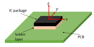
As shown previously, the displacements and accelerations of a plate under base excitation were obtained. As a result, it is now possible to analytically estimate solder interconnect stresses due to random vibration loadings. During this process, the number of solder joints for electronic system modelling is considered infinite. Thus, the interface layer can be assumed to be continuous, as shown in Figure 1, can be used to model this problem.
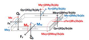
Considering the free-body diagrams of the interconnect shown in Figure 2 and with assuming that the normal stress and shear stress are constant throughout the thickness of the solder, and the value of the linear bending moment the electronic component is equal to m1, and at the PCB is m2 their equations can be written as:
$m_{2 x}=r_x m_{1 x}$ (25)
$m_{2 y}=r_y m_{1 y}$ (26)
Figure 1. Electronic assembly details
Figure 2. Free-body diagrams for the solder interconnect moments and shear forces [8]
where, $r_x$ and $r_y$ are constants related to the bending and shear deformations of the interconnect. The moments $m_1$ and $m_2$ discussed previously are composed into two moment components as $m_\phi$ which represents the pure bending state of the solder and the second component $m_s$ which creates a cut along the length of the solder and varies linearly across the solder length. Both moments have $x$ and $y$ components and are written as:
$m_{\phi x}=\frac{m_{2 x}-m_{1 x}}{2}$ and $m_{\phi y}=\frac{m_{2 y}-m_{1 y}}{2}$ (27)
$m_{s x}=\frac{m_{2 x}+m_{1 x}}{2}$ and $m_{s y}=\frac{m_{2 y}+m_{1 y}}{2}$ (28)
The normal force (fn(x)), shear force (fs(x)) and the bending moment (mϕ(x)) can be expressed in terms of the equivalent normal stiffness (kn), shear stiffness (ks) and flexural stiffness (kϕ) of the solder interconnect, as:
$f_n(x)=k_n \times \delta_n$ (29)
$f_s(x)=k_s \times \delta_s$ (30)
$m_\phi(x)=k_\phi \times \phi$ (31)
where, δn, δs and ϕ are the normal, shear and flexural deformations of the interconnect, respectively.
Define the solder stiffnesses as
$k_n=\frac{n E_s A_S}{h_s}$ (32)
$k_s=\frac{n G_s J_s}{h_s}$ (33)
$k_\phi=\frac{n E_s I_s}{h_s}$ (34)
where, n is the number of the solder joints in the electronic structure; Es and Gs are the tensile and shear moduli of the solder material, respectively; As, Js and Is and hs are the cross-sectional area, polar moment of inertia and second moment of area and the standoff length of the solder interconnect, respectively.
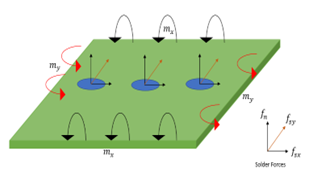
Considering the free-body diagram of the PCB when exposed to bending due to random vibrations, as shown in Figure 3, the PCB moments are written in the function of the solder moments (Figure 4) as:
$m_x+\int m_{1 x} d x=D\left(\frac{\partial^2 w}{\partial x^2}+v \frac{\partial^2 w}{\partial y^2}\right)$ (35)
$m_y+\int m_{1 y} d y=D\left(\frac{\partial^2 w}{\partial y^2}+v \frac{\partial^2 w}{\partial x^2}\right)$ (36)
$m_{x y}=D(v-1) \frac{\partial^2 w}{\partial x \partial y}$ (37)
where, D and ν are the flexural rigidity and Poisson’s ratio of the PCB material. Similarly, solder shear and normal forces can be expressed as:
$f_{s x}=\frac{m_{2 x}+m_{1 x}}{h_s}=\frac{2 m_{s x}}{h_s}$ (38)
$f_{s y}=\frac{m_{2 y}+m_{1 y}}{h_R}=\frac{2 m_{s y}}{h_s}$ (39)
Figure 3. Free body diagram of the PCB when exposed bending due to random vibrations [21]
Figure 4. Solder interconnect state of bending, normal forces, and shear forces when the PCB is subjected to bending due to random vibration
Generally, the solder normal stresses are expressed by substituting Eq. (29) and Eq. (32) into Eq. (11), thus:
$\begin{gathered}\frac{\partial^4 f_n}{\partial x^4}+2 \frac{\partial^4 f_n}{\partial x^2 \partial y^2}+\frac{\partial^4 f_n}{\partial y^4}-A \frac{\partial^4 f_n}{\partial x^2}-B \frac{\partial^4 f_n}{\partial y^2}-C f_n-D=0\end{gathered}$ (40)
A, B, C and D are constant coefficients depends on the solder geometry.
Therefore, the equivalent sum of the solder normal stresses due to base acceleration is:
$\int_0^L \int_0^W f_n d x d y=m_{1 c} a$ (41)
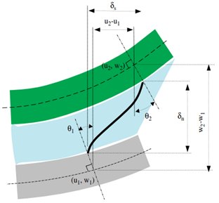
L and W are, respectively, the symmetrical length and width of the IC component. Considering Figure 5, the slopes of the horizontal and vertical axes are going to be equal to zero, such as:
$\frac{\partial \delta_n}{\partial x}(x, 0)=0 \rightarrow \frac{\partial f_n}{\partial x}(x, 0)=0$ (42)
$\frac{\partial \delta_n}{\partial y}(0, y)=0 \rightarrow \frac{\partial f_n}{\partial y}(0, y)=0$ (43)
Thus, the curvature differences between the IC package and circuit board shown in Figure 5 is:
$\frac{\partial^2 f_n}{\partial x^2}=\frac{k_n}{R M S\left(R_{x P S R}\right)}$ (44)
$\frac{\partial^2 f_n}{\partial y^2}=\frac{k_n}{R M S\left(R_y P C B\right)}$ (45)
where, RMS(RxPCB) and RMS(RyPCB)are the root-mean-squares of the solder normal stresses along the x and y directions, which can be evaluated using the method of the repetition of the changes [3] such as:
$R M S\left(R_{x P C B}\right)=\iint m_x d x d y$ (46)
$R M S\left(R_{x P C B}\right)=\iint m_y d x d y$ (47)
Figure 5. The deformed shape of the solder interconnect due to mechanical bending [22]
Similarly, the root mean squares of the normal stress (σn) and the bending stress (σb) of the interconnection are:
$R M S\left(\sigma_n\right)=\sqrt{R M S\left(m_x\right)^2+R M S\left(m_y\right)^2}$ (48)
$\operatorname{RMS}\left(\sigma_b\right)=\frac{R M S\left(\sigma_n\right) \times R_S}{I_s}$ (49)
where, Rs is the solder maximum radius and Is the cross=sectional second moment of inertia around the solder neutral axis.
In order to validate the current analytical solution, it was compared with the finite element solutions. In this validation, an electronic assembly with the mechanical and geometrical properties listed in Table 1 are considered. In this validation system, 20 symmetrically distributed solder interconnections are used to attach the circuit board with the integrated package. The loading condition is base acceleration excitation with random vibration white noise profile of 0.5 PSD in the frequency range of 20 to 2,000 Hz.
Table 1. Mechanical and geometrical details of electronic system used in the validation study
|
Specifications |
Electronic Board |
Electronic Unit |
Solder Connection |
|
Length (cm) |
16 |
4 |
- |
|
Width (cm) |
8 |
2 |
- |
|
Height (cm) |
0.1 |
0.4 |
0.1 |
|
Radius (cm) |
- |
- |
0.1 |
|
Young's modulus (GPa) |
22.5 |
27 |
42.5 |
|
Density (×103 kg/cm3) |
2680 |
1035 |
8410 |
|
Poisson's ratio |
0.12 |
0.3 |
0.4 |
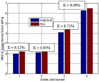
Figure 6. Analytical solution validation with FEA results in terms of solder RMS stress value
For the finite element analysis (FEA) modelling, ANSYS version 17 is used. For the element type, SOLID185 element is used for modelling the board, package and solder balls. The previously described properties and loading conditions are also applied in this simulation. The results of the FEA modelling are compared to those of the analytical model as shown in Figure 6. The relative error (E) between FEA and the analytical solution results are also included in the figure. In this comparison, only the first 4 solders in the system were compared as they the most important and crucial interconnects.
The results of this validation study show that the root mean square stresses of the considered solder interconnects from the analytical solutions and the FEA numerical solutions are in great agreement with an approximate relative error less than 10%. Thus, this solution is accurate and effectively compute, evaluate, and predict solder stresses due to random vibrations.
This investigation has presented an analytical exploration of the random vibration loads imposed on electronic boards. The board, throughout the course of this study, has been conceptualized as a multi-layered assembly of elastic rectangular plates, encompassing the board itself, the solder layer, and the package.
An in-depth examination of solder joint stresses and potential failure due to random vibration loading was conducted, and the influence of problem parameters, including the board's width and the imposed boundary conditions, was assessed. The findings revealed that solder joints of shorter lengths are subjected to reduced stress, suggesting an enhanced reliability under random vibration conditions. It was also determined that the fatigue life of solder joints could be significantly improved through stiffer PCB designs and smaller packages.
Finally, the analytical solution was corroborated with finite element simulations, with a deviation of less than 10%. This validation provides confidence in the effectiveness of the proposed analytical approach.
This study contributes to the body of knowledge on electronic board resilience against random vibrations, offering valuable insights for the design and manufacture of more robust and reliable electronic components. Future work could further investigate different material properties and their impact on stress distribution, expanding the generalizability of these findings to a wider range of electronic packages.
[1] Volkersen, O. (1938). Die Nietraftverteilung in Zugbeanspruchten Nietverblendugen mit Knastaten Laschenquerschntlen. Luftfahrt Forsch., 15: 4116. https://doi.org/10.31399/asm.hb.v08.9781627081764
[2] Goland, M., Reissner, E. (1944). The stresses in cemented joints. Applied Mechanics, 1(11): A17-A27. https://doi.org/10.1115/1.4009336
[3] Gharaibeh, M.A., Pitarresi, J.M. (2023). An efficient equivalent static methodology for simulating electronic packages subjected to resonant vibrations. Microelectronics Reliability, 145: 115000. https://doi.org/10.1016/j.microrel.2023.115000
[4] Wong, E.H. (2016). Design analysis of sandwiched structures experiencing differential thermal expansion and differential free-edge stretching. International Journal of Adhesion and Adhesives, 65: 19-27. https://doi.org/10.1016/j.ijadhadh.2015.10.021
[5] Wong, E.H., Mai, Y.W. (2006). New insights into board level drop impact. Microelectronics Reliability, 46(5-6): 930-938. https://doi.org/10.1016/j.microrel.2005.07.114
[6] Wong, E.H., Mai, Y.W., Seah, S.K., Lim, K.M., Lim, T.B. (2007). Analytical solutions for interconnect stress in board level drop impact. IEEE Transactions on Advanced Packaging, 30(4): 654-664. https://doi.org/10.1109/TADVP.2007.898599
[7] Wong, E.H., Mai, Y.W., Seah, S.K.W., Lim, K.M., Lim, T.B. (2006). Analytical solutions for interconnect stress in board level drop impact. In 56th Electronic Components and Technology Conference 2006, San Diego, CA, USA. https://doi.org/10.1109/ECTC.2006.1645905
[8] Larbi, A.S., Ferrier, E., Jurkiewiez, B., Hamelin, P. (2007). Static behaviour of steel concrete beam connected by bonding. Engineering Structures, 29(6): 1034-1042. https://doi.org/10.1016/j.engstruct.2006.06.015
[9] Engel, P.A. (1990). Structural analysis for circuit card systems subjected to bending. Journal of Electronic Packaging, 112(1): 2-10. https://doi.org/10.1115/1.2904336
[10] Pitarresi, J.M., Ceurter, J. (1999). Elasticly coupled beams loaded by a point force. In 13th Engineering Mechanics Conference, Baltimore, MD, June, pp. 13-16.
[11] Gharaibeh, M.A., Liu, D., Pitarresi, J.M. (2017). A pair of partially coupled beams subjected to concentrated force. IEEE Transactions on Components, Packaging and Manufacturing Technology, 7(8): 1293-1304. https://doi.org/10.1109/TCPMT.2017.2670019
[12] Gharaibeh, M.A., Ismail, A.A., Al-Shammary, A.F., Ali, O.A. (2019). Three-material beam: Experimental setup and theoretical calculations. Jordan Journal of Mechanical & Industrial Engineering, 13(4): 253-264.
[13] Gharaibeh, M.A., Almohammad, A.A. (2022). Numerical solution for electronic assemblies subjected to mechanical bending. Mathematical Modelling of Engineering Problems, 9(1): 51-59. https://doi.org/10.18280/mmep.090107
[14] Gharaibeh, M.A. (2015). Finite element modelling, characterization and design of electronic packages under vibration. PhD Dissertation, State University of New York at Binghamton.
[15] Gharaibeh, M.A. (2018). Reliability analysis of vibrating electronic assemblies using analytical solutions and response surface methodology. Microelectronics Reliability, 84: 238-247. https://doi.org/10.1016/j.microrel.2018.03.029
[16] Gharaibeh, M.A., Su, Q.T., Pitarresi, J.M. (2018). Analytical model for the transient analysis of electronic assemblies subjected to impact loading. Microelectronics Reliability, 91: 112-119. https://doi.org/10.1016/j.microrel.2018.08.009
[17] Gharaibeh, M. (2018). Reliability assessment of electronic assemblies under vibration by statistical factorial analysis approach. Soldering & Surface Mount Technology, 30(3): 171-181. https://doi.org/10.1108/SSMT-10-2017-0036
[18] Gharaibeh, M.A., Pitarresi, J.M. (2019). Random vibration fatigue life analysis of electronic packages by analytical solutions and Taguchi method. Microelectronics Reliability, 102: 113475. https://doi.org/10.1016/j.microrel.2019.113475
[19] Wiener, N. (1930). Generalized harmonic analysis. Acta Mathematica, 55(1): 117-258. https://doi.org/10.1007/BF02546511
[20] Wirsching, P.H., Paez, T.L., Ortiz, K. (2006). Random Vibrations: Theory and Practice. Courier Corporation.
[21] Hosseinloo, A.H., Yap, F.F., Vahdati, N. (2013). Analytical random vibration analysis of boundary-excited thin rectangular plates. International Journal of Structural Stability and Dynamics, 13(3): 1250062. https://doi.org/10.1142/S0219455412500629
[22] Gharaibeh, M.A., Su, Q.T., Pitarresi, J.M. (2016). Analytical solution for electronic assemblies under vibration. Journal of Electronic Packaging, 138(1): 011003. https://doi.org/10.1115/1.4032497
[23] Rao, S.S. (2019). Vibration of Continuous Systems. John Wiley & Sons.