OPEN ACCESS
We evaluated the performance of a hardware architecture designed to perform a wide range of fast image processing tasks. The system architecture is based on hardware featuring a Field Programmable Gate Array (FPGA) co-processor and a host computer. A host application controlling a frame grabber and an industrial camera is used to capture and exchange video data with the hardware co-processor via a high speed USB3.0 channel, implemented with a standard macrocell, The FPGA accelerator is based on a XILINX kintex-7 chip and is designed as a system-on-a-programmable-chip with the help of an embedded software processor. The SOPC system integrates the CPU, external and on chip memory, the communication channel and typical image filters appropriate for the evaluation of the system performance. Measured transfer rates over the communication channel and processing times for the implemented hardware logic are presented for various frame sizes. A comparison with other solutions is given and a range of application is also discussed.
field programmable gate array, image filters, universal serial bus, system-on-a-programmable-chip
The traditional hardware implementation of image processing uses Digital Signal Processors (DSP) or Application Specific Integrated Circuits (ASIC). However, the growing need for faster and cost-effective systems triggers a shift to Field Programmable Gate Arrays (FPGA), where the inherent parallelism results in better performance. When an application requires real-time processing, like video or television signal processing or real-time trajectory generation of a robotic manipulator, the specifications are very strict and are better met when implemented in hardware. Computationally demanding functions like convolution filters, motion estimators, two-dimensional Discrete Cosine Transforms (2D DCT) and Fast Fourier Transforms (FFT) are better optimized when targeted on FPGA [1-4]. Features like embedded hardware multipliers, increased number of memory blocks and system-on-a-chip integration enable video applications in FPGA that can outperform conventional DSP designs.
On the other hand, solutions to a number of imaging problems are more flexible when implemented in software rather than in hardware, especially when they are not computationally demanding or when they need to be executed sporadically in the overall process. Moreover, some hardware components are hard to be re-designed and transferred on a FPGA board from scratch when they are already a functional part of a computer-based system. Such components are frame grabbers and multiple-camera systems already installed as part of an imaging application or other robotic control equipment.
Following the above considerations we conclude that it is often needed to integrate components from an already installed computer-based imaging application dedicated to some automation system, with FPGA-based accelerators that exploit the low-level parallelism inherent in hardware structures. Thus a critical need arises for an embedded software/hardware interface that can allow for high-bandwidth communication between the host application and the hardware accelerators.
In this paper we apply and evaluate the performance of an example mixed hardware design that includes on the one side a host computer running imaging application, equipped with a camera and a frame-grabber, and on the other side a XILINX FPGA board [5] running an image filter hardware accelerator and other system components. The communication channel transferring image data from the host computer to the hardware board is a high-speed USB3.0 port. The various hardware parts and external circuit on the FPGA board are controlled. As a result of this evaluation one can explore the range of applications suitable for a host/co-processor architecture including an embedded processor and utilizing a USB3.0 communication channel.
In the following, we first give a short account of the tools we used for system design. We also present an overview of the particular image filtering application we embedded in the FPGA chip for the evaluation of the host/co-processor system architecture. We describe the modular interconnection of different system parts and assess the performance of the system. We examine the speed and frame-size limits of such a design when it is dedicated to image processing finally.
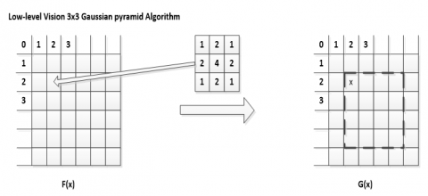
Low-level Vision 3x3 Gaussian pyramid Algorithm: two dimensional low-pass filters, such as the Gaussian low-pass filter, work with a filter kernel, calculate an average value for a destination pixel using a number of neighboring source pixels. The two dimensional Gaussian filter is shown in following figure1.
When dealing with digital images integer weighting factors are used. A typical 3x3 Gaussian filter matrix and the decimation of the pixels are shown in Figure 1. The anchor point of the Gaussian filter kernel is marked with an “X”.
Figure 1. Gaussian pyramid filter 3x3 kernel
Obviously for every calculated pixel one neighboring pixels in both dimensions are required. Therefore, this function uses a Region of Interest (ROI). With every Gaussian pyramid level the number of pixels in x- and y-coordinates is reduced by a factor of 1.
According to Gaussian calculation method for using the neighbor pixels window 3x3 or 5x5 to get the new pixel data, taking into consideration that their differences in their kernel’s size. Taking into consideration that; expressing the kernel operation in each frame process can be decomposed into block processing mode, and this block has the same processing function and the number and size determine degree of algorithm parallelism.
The degree of parallelism for one (256x256) image frame is 256x3 or 256x5 delay element blocks respectively with. Computing time is determined by number of machine cycle to get the first frame pixel plus number of a whole frame pixels calculated in the pipe line, total number of machine cycles = 9 + 256*256 = 65,545 machine cycle. Working with frequency 100MHz (10nSec) we found that time = 10nSec * 65,545 = 0.6554 mSec almost 0.66 mSec for single frame. So from that; we defined a new general structure design of fast image processing as we will explain later. This process and technique for Gaussian 3x3 and Gaussian 5x5 will have the same speed of calculations versus using a little more of FPGA utilization resources.
Edge detection is the name for a set of mathematical methods which aim at identifying points in a digital imageat which the image brightness changes sharply or, more formally, has discontinuities. The points at which image brightness changes sharply are typically organized into a set of curved line segments termed edges. The same problem of finding discontinuities in 1D signal is known as step detection and the problem of finding signal discontinuities over time is known as change detection. Edge detection is a fundamental tool in processing, machine and computer vision, particularly in the areas of feature detection and feature extraction.
The purpose of detecting sharp changes in image brightness is to capture important events and changes in properties of the world. It can be shown that under rather general assumptions for an image formation model, discontinuities in image brightness are likely to correspond to: discontinuities in depth; discontinuities in surface orientation; changes in material properties and variations in scene illumination.
The design of a DSP system with FPGA often utilizes both high-level algorithm development tools and hardware description language (HDL) tools. It can also make use of third-party intellectual property (IP) cores implementing typical DSP functions or high speed communication protocols.
In our application we use model-based design tools like The Math works Simulink (based on Math work’s MATLAB) with the libraries of XILINX’s IP core. The core uses model design to produce and synthesize HDL code, which can then be integrated with other hardware design files within a synthesis tool, like the ISE 14.4 development environment. In the present work, we designed image filter components using IP libraries and the resulting blocks were integrated with the rest of the system in XILINX’s Embedded Development Kit (EDK) Builder.
EDK-Builder design software resides as a tool in the XILINX environment [6]. Its purpose is to integrate an embedded software processor like Platform Studio (XPS) with hardware logic and custom or standard peripherals within an overall system, often called Embedded Development Kit (EDK). EDK-Builder provides an interface fabric in order to interconnect the Platform Studio processing path with embedded and external memory, the filter co-processors, other peripherals and the channels of communication with the host computer.
On the host side one may develop a control application by means of any suitable language like C. We use software by National Instruments Corporation [10], which provides a very flexible platform for image acquisition, image processing and industrial control.
The proposed methodology and its corresponding architecture for the image processing are illustrated in Fig. 2. It describes the architecture in the camera in which data acquisition; signal processing and communication capabilities are embedded.
The main target of this work is to evaluate the performance of a host/co-processor architecture including an embedded processor and utilizing a communication channel between host and hardware board, like a USB3.0 channel. The task-logic performed by the embedded accelerator can be any image function within the limitations of existing FPGA devices.
For our purpose we built a typical image-processing application in order to target the FPGA co-processor. It consists of a noise filter followed by an edge-detector. Noise reduction and edge detection are two elementary processes required for most machine vision applications, like object recognition, medical imaging, lane detection in next-generation automotive technology, people tracking, control systems, etc.
Figure 2. System architecture
We model noise and edge filtering using the XILINX’s DSP Libraries in Simulink. An example of this procedure can be found in. Noise reduction is applied with a Gaussian 3x3 kernel while edge detection is designed using typical Prewitt or Sobel filters. These functions can be applied combined in series to achieve edge detection after noise reduction. Apart from noise and edge filter blocks, there is also a block representing the intermediate logic between the MicroBlaze data and control paths and our filter task logic. Such intermediate hardware fabric follows a specific protocol referred to as Avalon interface. This interface cannot be modeled in the Simulink environment and is rather inserted in the system as a verilog file. Design examples implementing the Avalon protocol can be found in XILINX reference designs and technical reports. In brief, our Avalon implementation consists of a 16-bit data-input and output path, the appropriate Read and Write control signals and a control interface that allows for selection between the intermediate output from the Gauss filter and the output from the edge detector. Data input and output to and from the task logic blocks is implemented with the help of Read and Write instances of a 4800 bytes FIFO register.
Each image frame when received by the hardware board is loaded into an external SDRAM memory buffer and is converted into an appropriate 16-bit data stream by means of MicroBlaze instruction code. Data transfer between external memory buffers and the MicroBlaze data bus is achieved through Direct Memory Access (DMA) operations controlled by appropriate instruction code for the MicroBlaze soft processor.
Incoming pixels are processed by means of a simple 2D digital Finite Impulse Response (FIR) filter convolution kernel, working on the gray scale intensities of each pixel’s neighbors in a 3x3 region. Image lines are buffered through delay-lines producing primitive 3x3 cells where the filter kernel applies. A delay block produces a neighboring pixel in the same scan line, while a 640 delay block produces the neighboring pixel in the previous image scan line. We assume
image size of 640x480 pixels. The line-buffer circuit is implemented in the same manner for both noise and edge filters. Frame resolution is incorporated in the line-buffer diagram as a hardware built-in parameter. If a change in frame size is required we need to re-design and re-compile. The number of delay blocks depends on the size of the convolution kernel, while delay line depth depends on the number of pixels in each line. Each incoming pixel is at the center of the mask and the line buffers produce the neighboring pixels in adjacent rows and columns. Delay lines with considerable depth are implemented as dedicated RAM blocks in the FPGA chip and do not consume logical elements.
After line buffering, pipeline adders and embedded multipliers calculate the convolution result for each central pixel. The model-design for implementation of the 3x3 Gauss kernel calculations. Logic-consuming calculations, like multiplications are implemented using dedicated multipliers available in medium-scale XILINX FPGA.
The co-processor parts described above were implemented as components of an embedded system controlled by a MicroBlaze processor, and are shown in Fig.3. The MicroBlaze software which is used here for data streaming control is often the basis for industrial as well as academic projects. It can be used in its evaluation version along with the tools for assembling and downloading instruction code. Once installed within the synthesis software, the MicroBlaze processor becomes integrated as a library component in XILINX’s EDK-builder tool.
EDK-Builder converts the model-based design into HDL code appropriate for integration with other hardware components. The filter is readily recognized by the synthesis software as a System-on-a-Programmable-Chip (SOPC) module and can be integrated within a MicroBlaze system with suitable hardware fabric [7]. Other modules that are necessary for a complete system are the MicroBlaze soft processor, external memory controllers, DMA channels, and a custom IP peripheral for high speed USB communication with the host. A VGA controller can be added in order to monitor the result on an external screen. Many of such peripheral functions can be found as open source custom HDL Intellectual Property (IP) or as evaluation cores provided by XILINX or third party companies.
USB 3.0 high speed connectivity is added to the FPGA board by means of a daughter-card by System Level Solutions (SLS) Corporation. It can be added to any XILINX board featuring a Santa-Cruz peripheral connector. This daughter-card provides an extension based on CY7C68000 PHY USB3.0 transceiver. A USB3.0 IP core compliant with Transceiver Macrocell Interface (UTMI) protocol allows integration of the USB function with the MicroBlaze system. We tested evaluation versions of the IP core and present practical transmit and receive rates. The FPGA chip along with the embedded MicroBlaze processor is always a slave device in the communication via the USB channel, while the host computer is always the master device.
The embedded system is assembled by means of the SOPC-Builder tool of the synthesis software, by selecting library components and defining their interconnection. After being generated by SOPC Builder, the system can be inserted as a block in a schematic file for synthesis and fitting processing. The only additional components that are necessary are PLLs for Nios and memory clocking. After we synthesize and simulate the design by means of the tools described in Section 2, we target a FPGA chip incorporated on a development board manufactured by Altera Corporation. The board also features external memory and several typical peripheral circuits.
Figure 3. EDK architecture
Integrated Software Environment (ISE14.4) software for FPGA and Matlab Math-works (R2011a) software both were used for design, validate and simulate our general structure fast image design, the FPGA embedded system used was from Xilinx Company product Kintex-7.
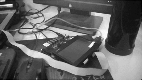
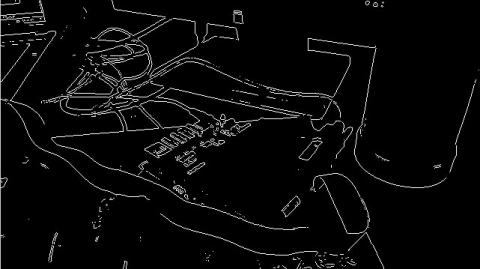
FPGA resources consummated due to our proposed design in Xilinx Kintex-7 number XC7K160T, that DSP48 slices is 2% in Gaussian kernel size 3x3 and 5% in Gaussian kernel size 5x5. Also umber of number of Digital Clock Manager (DCM) and other resources almost the same. Finally The main target is to see the both low level different kernel algorithm deals with real image with the size of 256x256 in figure 4-a and the output image result from applying Gaussian filter 3x3 shown in figure 4-b and edge filter result image in 4-c.
(c) Edge filter
Figure 4. Result of successive processing
The great advantage in our design implementation on FPGA is that whatever the kernel size and more usage of DSP48 slice the time difference is slightly change not the same as if we were using C language Programming technique, designing fast image algorithm main concerns is accuracy and reducing the time as minimum as possible which we applied the high accuracy by using DSP slice 18bit by 18 bit in multiplication and 48 bit in addition, in the other hand by using the implementation target is an FPGA instead of DSP we reduce the total image frame processing time.
The authors wish to thank National High Technology Research and Development Program. This work was supported in part by a grant from it.
1. W. J. MacLean, An Evaluation of The Suitability of Fpgas for Embedded Vision Systems, Proceedings of The 2005 IEEE Computer Society Conference On Computer Vision And Pattern Recognition (CVPR’05), vol.3, p. 131, California, USA, June 2005.
2. R. J. Petersen, B. L. Hutchings, An Assessment of the Suitability of FPGA-Based Systems for Use in Digital Signal Processing, 5th International Workshop on Field-Programmable Logic and Applications, pp. 293-302, Oxford, England, August 1995.
3. M. A. Vega-Rodriguez, J. M. Sanchez-Perez, J. A. Gomez-Pulido, Real Time Image Processing with Re-Configurable Hardware, 8th IEEE International Conference On Electronics, Circuits and Systems (ICECS2001), vol. 1, pp. 213-216, Malta, September 2001.
4. I. S. Uzun, A. Amira, A. Bouridane, FPGA Implementations of Fast Fourier Transforms for Real Time Signal and Image Processing, IEE Proceedings—Vision, Image and Signal Processing, 152(3), pp.283-296, 2005.
5. Edge Detection Using SOPC Builder and DSP Builder Tool Flow, Altera Technical Paper, AN-377-1.0, May 2005.
6. I. Y. Soon, C. K. Yeo, H. C. Ng, An Analogue Video Interface for General-Purpose DSP, Microprocessors and Microsystems 25, pp.33-39, 2001.