Shaina Gangadharan![]() | Ruqaiya Khanam*
| Ruqaiya Khanam*![]() | Veeraiyah Thangasamy
| Veeraiyah Thangasamy![]()
© 2024 The authors. This article is published by IIETA and is licensed under the CC BY 4.0 license (http://creativecommons.org/licenses/by/4.0/).
OPEN ACCESS
When it comes to the radio frequency (RF) frontend, power amplifier (PA) is one of the most important functional blocks for dependable wireless transmission. In order to provide the necessary output power, PAs boost and amplify the incoming signal, to ensure that the transmitter's signal reaches the receiver at the necessary distance. The PAs have not yet managed to find place within the transceiver circuit due to its bulky nature. Although rigorous efforts have been made to improve the linearity and efficiency of the PAs, it has come at the cost of increase in chip area. This paper focusses on design of an RFPA in an 18nm FinFET advanced node technology that is adaptable to the Sub-6 GHz frequency band of 5G communication standard so as to provide maximum output power at the operating frequency of 3.5GHz. The single stage PA, thus designed and simulated on Cadence Virtuoso provides a gain of 27.71 dB at a supply voltage of 1V. The bandwidth is 208 MHz, power gain is 25dB and the output power is 6.335 dBm. The simple design with a single transistor paves way for a considerable decrease in the chip area, thus making it possible to be placed within the transceiver chip.
radio frequency power amplifier, gain, output power, 5G, 3.5 GHz, bandwidth, Sub-6 GHz, 18nm FinFET technology
Since the first contemporary mobile phone systems were introduced, the wireless market has grown and developed remarkably, with a consistent rise in the number of subscribers, new application areas, and higher data rates. The effective high-level integration of electronic circuits in low-cost technologies is largely responsible for these achievements. Current trends in mobile communication system demands adaptability with the 5G and future communication systems while ensuring that the system parameters like the efficiency, output power, gain, bandwidth and operating frequency are within the standard limits and at the same time not compromising on the size of the frontend device. Mobile communication has been in a process of continuous evolution from decades and in its transformation from 4G to 5G various parameters has an impact on it and hence there is a need to adapt itself for the purpose of acceptability. One such block of the mobile communication system is the transceiver circuit in which the power amplifier plays a major role as it determines the efficiency of the transceiver. With evolution of future generation communication system, it has become necessary to design specification compatible circuits to work at low power. With inclusion of additional features and growing competition between mobile phone companies to gain market it has become necessary to enhance the technical performance of their products in terms of adaptability to the future generation communication system with wide bandwidths and high frequency bands of operation. Miniaturization is also a major aspect with a focus on improvement in the performance parameters. Technologies like FinFET, CNTFET, etc. are being proposed and continuous research is being carried out in this area to overcome the Moore’s theory. This paper aims at evaluating the performance parameters of analogue radio frequency (RF) power amplifier (PA) circuit designed using 18nm FinFET technology for mobile communication systems. Power Amplifier, the final stage of a transceiver circuit draws maximum power from the DC source thus reducing the efficiency of the entire circuit. With the advent of 5G, involving the sub-6GHz and mmW frequency ranges with bandwidth requirements around 200MHz, it has become a necessity to design low power high speed analog circuits using advanced technology [1]. PAs have to deal with high data rate signals due to which complex modulation techniques like Orthogonal Frequency Division Multiplexing (OFDM) has to be used, thus increasing the peak to average power ratio (PAPR). So reduced size and high PAPR pose constraints on improving the efficiency of the PA [2].
Another very important aspect is the miniaturization of the transmitter in RF communication, especially with the advent of 4G, due to which additional circuits supporting multimode multiband (MMMB) operation has been integrated. For 5G handsets, the RF front-ends pose three major constraints unlike the base station namely, limited circuit area, wideband operation and limited supply voltage [3]. To operate the PA at sub-6 GHz frequency for mobile communication low power CMOS techniques have been used with an intent of miniaturization. However, since the output power requirement is high, low node technologies pose constraints with respect to the permissible supply voltage, thus reducing the output power considerably. Over decades PA designs have been seen resorting to using efficiency enhancement methods to improve the drain efficiency and power added efficiency (PAE) while maintaining the linearity in circuit performance. Maintaining the efficiency while ensuring linearity in performance is a major challenge which has been a constraint while designing RF PAs. To overcome this designed various circuits to improve the efficiency and hence the PAE while maintaining the linearity [4-7], over a few decades CMOS technology has been used and there has been a revolution by scaling down from sub-micron to deep sub-micron (320nm to 45nm) for achieving low cost and high performance. However, scaling down CMOS gives rise to short channel effects and bulk CMOS gives rise to off-state leakage current [8]. Although CMOS transistors contribute to increased speed, it comes at the cost of degradation of transistors and in analog and RF circuits the decrease in intrinsic gain of the transistor adversely effects the performance [9]. Inspired by Hassanzadeh and Hadidi [10] for design of operational transconductance amplifier (OTA) and Singh et al. [11, 12] for power amplifier using FinFET, in this work we aim to improve the efficiency of the RFPA using conventional circuit with FinFET to operate in the sub-6 GHz frequency for 5G mobile communication.
The significance of this work lies in the design of an RF PA in an 18nm FinFET PDK available with Cadence Virtuoso, operating with VDD = 1 V. The reduction in supply voltage in comparison with the 3.3V requirement in CMOS technology, consequently reduces the power consumption. FinFETS have been extensively used for digital circuits and a few analog circuits. However, the work on design of RF PA is limited. The small size of FinFET will also reduce the die area required to fabricate the PA. The rest of the article is organised as follows. Section 2 describes the structure of FinFET Device and the drain current relationship with the various parameters of the physical structure of the FinFET. Section 3 provides a brief insight of the PA and the performance parameters associated with it. Sub section briefs about the small signal model and the extraction of the extrinsic and intrinsic elements which determine the performance of the PA at RF range of frequency. RF PA circuit design is covered in the subsequent subsection. Section 4 presents the results obtained by simulating the designed PA emphasising on the maximum gain at the operating frequency, the S parameters, bandwidth and output power. Section 5 summarises the outcome of the design and the possible recommendations to improve the performance parameters.
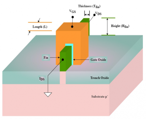
Unlike planar CMOS circuits, FinFETS are non-planar structures constructed on a silicon on insulator (SOI). Because of short channel effects and leakage when the gate length exceeds 22 nm, CMOS introduces noise and other unfavorable aspects. This results in a swing in the threshold voltage as well. A multigate device is used to replace this in order to precisely control the current flowing over the channel. A CMOS has a gate on only one side, whereas a FINFET, as depicted in Figure 1, has gates on three sides. These FETs are hence known as multigate FinFETs [13].
Figure 1. FinFET structure
The structure that resembles a fin and grows above the substrate is called a FinFET. They function far more efficiently than a conventional planar transistor for the same area because the "Fin" boosts the gate's control over current. Because the gate is long enough to govern the channel, it encircles the "Fin" and provides it additional authority over it. By reducing leakage current levels and improving electrostatic control over the channel area, this gate structure also helps to solve short-channel effect issues. Around a thin ridge of silicon of the order of 100nm in height a FinFET is built. Along this fin the carriers flow from source to drain. Since the gate electrode completely covers the underlying silicon nanowire, the electrostatic control of the gate voltage, VGS over the drain to source current, IDS is maximum. This further reduces the encroachment of the source to drain depletion region, thus reducing the SCEs [14].
The product of the fin height (Hfin) and fin thickness (Tfin) yields the effective width of the transistor Weff. Tfinis kept as narrow as possible to minimize the SCEs, resulting in an effective width that is almost equal to $2 H_{f i n}$. The portion of the fin which does not lie under the gate region is called the extension region and is considered to be a very important area as there is less possibility of the vertical side doping gradient to start from the highly doped source to drain region and finish at the lightly doped channel region [15].
$W_{e f f}=2 H_{f i n}+T_{\text {fin }}[15]$ (1)
Technology limitations pose constraints on changing the transistor height, thus the only possibility to increase the current is by increasing the number of fins. Hence if there are ‘n’ fins then, the effective width of the transistor is:
$W_{\text {eff }}=n \cdot 2 H_{\text {fin }}+n \cdot T_{\text {fin }}[15]$ (2)
Etching away the top gate side area of the transistor shown in Figure 1 results in two gates hence called Double gate transistor. Depending on how biasing is applied to the gates, a FinFET can operate in either an independent or symmetric driven mode. Due to their thin fin structure, the two gates in a double gate structure that receive biasing from one another also have an electrostatic influence on one another. The creation of a channel on the opposite side by the front gate may have an impact on the back gate's turn-on characteristics. The front gate bias voltage, Vthnf, is influenced by the rear gate bias voltage, Vgb, and vice versa. The relationship is depicted by Eq. (3).
$V_{t h n f}=V_{t h n}-r * V_{g b}[15]$ (3)
where, the gate-to-gate coupling coefficient, r is given in Eq. (4):
$r=\frac{3 * T_{o x f}}{3 * T_{o x b}+T_{s i}}[15]$ (4)
where Tsi indicates the silicon thickness and Toxf and Toxb, respectively, represent the oxide thickness of the front and rear gates. In low power mode, the back gate experiences a negative bias, raising the front gate's threshold voltage and lowering the transistor's leakage current as a result. Eq. (5) represents the subthreshold current of the FinFET:
$I_{d s}=\propto * \frac{W}{L} * e^{\frac{V_{G S} V_{t h n}-0.473 V_{g b}}{\beta}} *\left(1-e^{\left(\frac{-q_* V_{D S}}{k T}\right)}\right)[15]$ (5)
where 0.473 is derived by replacing the standard values of Toxf , Toxb and Tsi, in Eq. (4), α, β are the coefficient, k is the Boltzmann constant and T is the temperature. If the back gate is grounded then the current is only dependent on the gate to source voltage and the threshold voltage. For future VLSI technologies, involving both analog RF applications and digital circuits like non-volatile memories, FinFET has been considered and investigation is in progress in terms of its System-on-chip (SoC) possibilities. The most difficult challenge with RF power amplifiers is requiring high output power while keeping linearity and efficiency. It has also not been feasible to integrate the power amplifier into the transceiver circuit because of the large size of the inductors and the practicality of employing CMOS transistors with low scaling. The FinFET delivers greater SS and stronger drive strength for moderate gate voltages (0.2-0.4V) while maintaining the same IOFF (i.e. leakage) characteristics as a planar device. For low-voltage analog designs, this leads to better transconductance (gm) and improved switching speed for digital systems. This is helpful for low-frequency analog and digital designs, but it doesn't reveal anything about a FinFET process's mmWave and Sub-6 GHz frequency capabilities. The challenge in this work is to optimize the FinFET in order to obtain maximum drain current and thus the output power at 3.5 GHz frequency. The device's performance and local interconnect dependability are impacted by the temperature rise brought on by self-heating effects. Therefore, there must be a trade-off between reliability and performance when limiting the power across a device, either by running at lower current densities or supply voltages. Thankfully, this tradeoff is not as severe because the FinFET can continue to operate dynamically at lower supply voltages.
The last block in the transciever circuit is the power amplifier which is the most power consuming component, resulting in low efficiency. It has been a challenge to integrate all the blocks of the transciever on a single chip, due to the constraints on using same semiconductor material. PA's are normally designed using III-V compound semiconductors, irrespective of the high cost due to its capacity to deliver high linear output power with respect to silicon, while all the other blocks are designed in CMOS thus resulting in dual chip implementation [16]. In view of improving the gain, speed, efficiency and the PAE while reducing the area requirement and noise, downscaling of CMOS in the nanoscale range has been experimented over decades [17]. A large database of analog RF PA circuits is available which has been designed using various topologies in Class A, Class B, Class C, Class AB in linear mode and Class D, Class E, Class F etc. in the non linear mode. Power enhancement techniques like Doherty, Envelope Elimination and Restoration (EER) and Envelope Tracking (ET) are the most popularly used methods to improve the efficiency of the PA. There has also been a constant demand to integrate as many circuits into a single chip as possible for designing compact devices. Although a challenge, PA circuits have been designed in CMOS Technology using various topologies and enhancement methods as suggested by Bameri et al. [18-23] and many more papers depicting the same objectives. All these work focus on a frequency within the 4G communication range. With the advent of 5G and future generation communication it has become highly necessary to design circuits compatible to deliver standard results in the specific frequency bands.PA performance is assessed using a variety of factors. Linearity, power consumption, power added efficiency (PAE), output power, and power gain are the most significant features of a PA design. The tradeoff between the efficiency and linearity has been a concern while designing PA.
Common definitions of parameters under measurement:
$P_{\text {out }}=\frac{V_{\text {out }}^2}{R_L}$ (6)
where, Vout and RL are the output voltage load resistance respectively
$P_{\text {Total }}=P_S+P_D$ (7)
$G=10 \log _{10} \frac{P_{\text {out }}}{P_{\text {in }}} d B$ (8)
where, Pout and Pin are the output and input powers respectively.
Drain efficiency (DE): Is calculated by dividing the output RF power by the dissipated DC power.
$D E=\frac{P_{\text {out }}}{P_{(D C, \text { drain })}}$ (9)
Power Added Efficiency (PAE): Is measured by calculating the difference between the output and the input powers and dividing it by the dissipated DC power,
$P A E=\frac{\left(P_{\text {out }}-P_{\text {in }}\right)}{P_{(D C, \text { drain })}}$ (10)
3.1 Block diagram
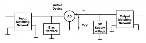
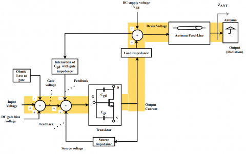
Figure 2 shows the generalized structure of the PA. The active device is the transistor and the matching network at the input and output side ensures maximum power transfer. Assuming that the output of the PA terminates into a load which is most often a transmission line connected to an antenna it is impossible to optimize the load impedance to ensure high efficiency and linearity. Thus, an output network like a tank circuit or a transformer is used to transform the real load impedance to the optimum output load resistance for amplifying devices.
Figure 2. Block diagram of PA
The bias network is responsible for providing the proper bias for operating the transistor as an amplifier. The operation of the PA is characterized by the output power, class of operation, intended frequency of operation and the circuit configuration. The individual power transistors available are capable of providing output power approximately equal to 150 W due to its inability to handle the current and voltage levels required for RF amplifications to higher levels and also the fact that the heat dissipation needs to be properly handled.
3.2 Analysis of the small signal model of FinFET
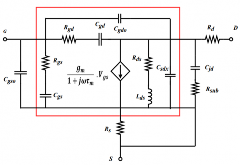
When building a PA at RF frequencies, it is imperative to analyze the corresponding model of the active device. The FinFET microwave model consists of three models: a small signal, noise, and large signal model. The small signal model serves as the foundational model and is generated from the other two models [24]. The circuit is separated into two sections, extrinsic and intrinsic (within the red box), according to their dependency or independence on the external bias, in Figure 3, which depicts a small signal equivalent of the 3D model of the FinFET. The extrinsic elements are Cgs0, Cgd0, Rs, Rd, Rgs and Rgd that are defined as gate-to-source/drain parasitic capacitance, source and drain resistances and distributed channel resistances respectively.
Figure 3. Small signal equivalent of 3D FinFET
Cgd and Cgs are the gate-to-drain/source intrinsic parasitic capacitances, Rds is the output resistance, Lds and τm are responsible for the transport delay between the source and drain in short channel devices [25]. DIBL results in Csdx, gm is the transconductance and Cjd and Rsub are the capacitance and resistance induced due to substrate loss which varies in accordance with the substrate bias.
It is advisable to extract the extrinsic parameters first and for this the transistors are biased under OFF state. The circuit in Figure 3 thus reduces to that shown in Figure 4.
The Y-parameter model is analyzed by Qin et al. [24] in the OFF state and the real and imaginary parts are represented as shown in Eqs. (11)-(14).
$\operatorname{Im}\left[Y_{12}\right]=\frac{N_{10} \omega+N_{11} \omega^3+N_{12} \omega^5}{1+M_{11} \omega^2+M_{12} \omega^4+M_{13} \omega^6}$ (11)
$\operatorname{Re}\left[Y_{12}\right]=\frac{N_{20} \omega^2+N_{21} \omega^4+N_{22} \omega^6}{1+M_{11} \omega^2+M_{12} \omega^4+M_{13} \omega^6}$ (12)
$\operatorname{RIm}\left[Y_{22}\right]=\frac{N_{30} \omega+N_{31} \omega^3+N_{32} \omega^5}{1+M_{11} \omega^2+M_{12} \omega^4+M_{13} \omega^6}$ (13)
$\operatorname{Re}\left[Y_{22}\right]=\frac{N_{40} \omega^2+N_{41} \omega^4}{1+M_{11} \omega^2+M_{12} \omega^4+M_{13} \omega^6}$ (14)
where, the coefficients Nij and Mij are all the functions of the elements shown in Figure 4. The coefficients N10 to N40 are defined as follows:
$N_{10}=C_{g d o}$ (15)
$N_{20}=C_{g d o}\left(C_{g d o}+C_{j d}\right) R_s$ (16)
$N_{30}=C_{g s o}+C_{j d}$ (17)
$N_{40}=\left(C_{g s o}+C_{j d}\right)^2 R_s+C_{j d}^2 R_{s u b}$ (18)
The symmetry of the device structure suggests that $C_{g s o}=C_{g d o}, R_s=R_d$ and the extrinsic parameters can be extracted as follows:
$C_{g s o}=C_{g d o}=N_{10}$ (19)
$C_{j d}=N_{30}-N_{10}$ (20)
$R_s=R_d=N_{20} / N_{10} N_{30}$ (21)
$R_{\text {sub }}={ }^{\left(N_{40}-\frac{N_{30}^2 N_{20}}{N_{10} N_{30}}\right)} /_{\left(N_{30}-N_{10}\right)^2}$ (22)
If the effect of the extrinsic parameters is excluded, then the Y-parameters of the intrinsic equivalent circuit:
Short circuit input admittance,
$Y_{11}=\frac{j \omega C_{g s} * \frac{1}{R_{g s}}}{j \omega C_{g s}+\frac{1}{R_{g s}}}+\frac{j \omega C_{g d} * \frac{1}{R_{g d}}}{j \omega C_{g d}+\frac{1}{R_{g d}}}$ (23)
Short circuit transfer admittance from output to input port,
$Y_{12}=\frac{j \omega C_{g d^*} \frac{1}{R_{g d}}}{j \omega C_{g d}+\frac{1}{R_{g d}}}$ (24)
Short circuit transfer admittance from input to output port,
$Y_{21}=\frac{g_m}{1+j \frac{\omega}{\omega_0}} e^{-j \omega \tau_m}-\frac{j \omega C_{g d^*} \frac{1}{R_{g d}}}{j \omega C_{g d}+\frac{1}{R_{g d}}}$ (25)
Short circuit output admittance,
$Y_{22}=j \omega C_{s d x}+\frac{1}{R_{d s}+j \omega L_{d s}}+\frac{j \omega C_{g d^*} \frac{1}{R_{g d}}}{j \omega C_{g d}+\frac{1}{R_{g d}}}$ (26)
The real and imaginary parts of the admittance parameters are derived with respect to the angular frequency, ω as shown in the Eqs. (27)-(34).
$\operatorname{Im}\left[Y_{11}+Y_{12}\right]=\frac{K_{10} \omega}{1+K_{11} \omega^2}$ (27)
$\operatorname{Re}\left[Y_{11}+Y_{12}\right]=\frac{K_{20} \omega^2}{1+K_{11} \omega^2}$ (28)
$\operatorname{Im}\left[-Y_{12}\right]=\frac{K_{30} \omega}{1+K_{31} \omega^2}$ (29)
$\operatorname{Re}\left[-Y_{12}\right]=\frac{K_{40} \omega^2}{1+K_{31} \omega^2}$ (30)
$\operatorname{Im}\left[Y_{21}-Y_{12}\right]=K_{50} \omega$ (31)
$\operatorname{Re}\left[Y_{21}-Y_{12}\right]=K_{60}+K_{61} \omega^2$ (32)
$\operatorname{Im}\left[Y_{12}+Y_{22}\right]=\frac{K_{70} \omega+K_{71} \omega^3}{1+\frac{L_{d s}^2}{R_{d s}} \omega^2}$ (33)
$\frac{1}{\operatorname{Re}\left[Y_{12}+Y_{22}\right]}=K_{80}+K_{90} \omega^2$ (34)
The coefficients represented as Kij are:
K_{10}=C_{g s} (35)
$K_{20}=C_{g s}^2 R_{g s}$ (36)
$K_{30}=C_{g d}$ (37)
$K_{40}=C_{g d}^2 R_{g d}$ (38)
$K_{50}=g_m \tau_m$ (39)
$K_{60}=g_m$ (40)
$K_{70}=C_{s d x}-\frac{L_{d s}}{R_{d s}^2}$ (41)
$K_{80}=R_{d s}$ (42)
$K_{90}=\frac{L_{d s}^2}{R_{d s}}$ (43)
From the simulation results obtained by Kang and Shin [25] and the Y-parameters the intrinsic small signal parameters can be depicted as:
$C_{g s}=K_{10}$ (44)
$R_{g s}=K_{20} / K_{10}^2$ (45)
$C_{g d}=K_{30}$ (46)
$R_{g d}=K_{40} / K_{30}^2$ (47)
$\tau_m=-K_{60} / K_{50}$ (48)
$g_m=K_{60}$ (49)
$C_{s d x}=N_{70}+\frac{\sqrt{K_{90} * K_{80}}}{K_{80}^2}$ (50)
$R_{d s}=K_{80}$ (51)
$L_{d s}=\sqrt{K_{90} * K_{80}}$ (52)
*All the expressions are from the analysis carried out by Qin et al. [24]:
Figure 4. Simplified equivalent circuit when no applied bias
This small signal model was tested by Qin et al. [24] for a 20nm FinFET and it was found that the model works perfectly for the frequency range from 10MHz to 300GHz in the linear region when Vgs = 1V and Vds = 0.1V and saturation region when both Vgs and Vds = 1V. With reference to the intrinsic parameters, it has been noticed that in the saturation region Cgs is much higher than Cgd, gm increases with increase in the drain voltage Vds and decreases with increase in gate voltage Vgs when the transistor moves towards the saturation region. Rds and Lds decreases with increasing values of Vgs, while $\tau_m$ increases for increasing values of Vds.
The intrinsic parameters are expected to improve the RF performance by substantially increasing the cutoff frequency fT, and the maximum frequency of oscillation fmax by reducing the values of Cgs, Cds, Rgs and Rgd. Scaling of FinFET is also an important aspect which contributes to the RF performance. The gate length Lg is responsible for increasing the Cgs and Cds due to the increasing plate area. This is compensated by the proportionality of the width to height of the fin such that the width is much smaller than twice the height of the fin. The increase in fin width and the value of Lg will also help to reduce Rgs and Rgd due to the change in effective cross-sectional area of the gate to source/drain. The cutoff frequency fT, increases as Lg decreases and decreases as Wfin increases.
3.3 Design of RFPA
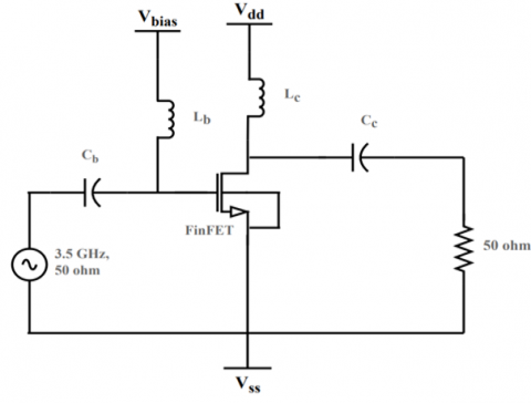
Of the various topologies available for the PA design the circuit here has been tested for a single stage transistor model. The major requirement for a PA is to minimize the tradeoff between efficiency and linearity which can be achieved by combining the properties of the Class A and Class B amplifiers [26]. Here in Figure 5, a single transistor model is designed to verify if the FinFET would be a suitable candidate to provide the required gain and power requirements. Figure 6 refers to the demonstration of the signal flow and the various parameters including parasitic that are present in the single transistor model of the PA.
The fundamental design factors pertain to the transistor's structure, including its channel length, gate width, suitable d.c. gate bias voltage, safe value of VDD for the chosen channel length, and a passive output matching network. Faster transistors have shorter channel lengths, which translate into greater maximum frequencies, or fmax, and maximum available gains (MAG) per stage. To ensure that the product is reliable, the value of VDD should guarantee Pout. The goal of reducing the d.c. gate bias is to increase the fmax and minimum gate width, which would be sufficient to add the Psat to the peak to average power ratio (PAPR) and total the Pout.
Figure 5. Single stage power amplifier circuit
Figure 6. Representation of signal flow and important parameters in a single-transistor PA stage
The Pout is limited by the safe value of VDD more than that of Imax. The design flow begins with the physical layout of the transistor in such a way that the extrinsic parasitic are controlled. In the process of d.c. to a.c. conversion in PA maximum PAE occurs only at Psat, but complex modulation techniques with high peak to average power ratio (PAPR) and error vector magnitude (EVM) requirements force a considerable backoff, thus causing the PAE to drop drastically. This can be improved by improving the ratio of Psat to the peak dissipated d.c power which depends on the technology, gate width, downscaling of safe Vdd with gate length. Static nonlinearities are exhibited by the voltage to current conversion of the transistor and the capacitances, Cgs and Cgd.
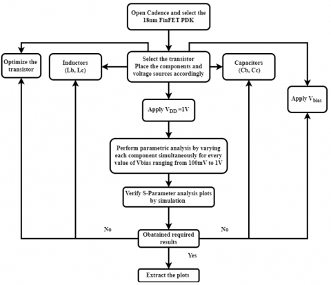
The flow diagram of the design process is shown in Figure 7.
Figure 7. Flow diagram of the design process
Table 1. Dimensions and parameters of simulated FinFET
|
Dimensions |
Values |
|
Transistor |
n1hvt |
|
Fin Pitch |
48nm |
|
Poly Pitch |
poly86 |
|
Gate Length |
18nm |
|
No. of Fingers |
1 |
|
Number of Fins per finger |
20 |
|
Multiplier |
70 |
Table 2. Values and dimensions of capacitance
|
Capacitor |
Dimensions |
Values |
|
Cc |
Plate capacitance |
1.025 mF |
|
Fringe capacitance |
242.5 pF |
|
|
Capacitor width |
1.019 µm |
|
|
Capacitor length |
3.6 µm |
|
|
Multiplier |
90 |
|
|
Capacitance |
6.00032 f F |
|
|
Cb |
Plate capacitance |
1.025 mF |
|
Fringe capacitance |
242.5 p F |
|
|
Capacitor width |
1.02 µm |
|
|
Capacitor length |
3.6 µm |
|
|
Multiplier |
15 |
|
|
Capacitance |
6.0045 f F |
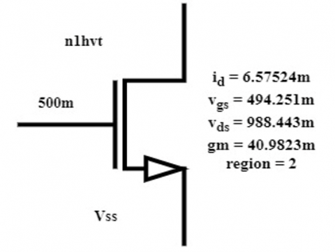
The PA is designed and simulated using Cadence Virtuoso design suite using 18nm FinFET technology. The n1hvt transistor characteristics are analysed using gm/Id method and the operating points are obtained. The transistor is biased so that it operates in region 2 with gm = 40.9823m, Vgs = 494.251mV and Id = 6.57524mA and Vds = 988.443mV. The main geometric parameters of the FinFET are fin length, fin width, oxide thickness and fin height. The FinFET is optimized by varying the number of fins and multiplier the simulated dimensions and parameters of which are shown in Table 1. The circuit is operated at supply voltage, VDD = 1V and bias voltage, Vbias = 500mV. Through parametric analysis the values of the inductors and capacitors in the input and output matching networks are determined in such a way that maximum gain is centered at 3.5GHz frequency. The input matching network comprises of a capacitor Cb and Lb and the output matching network comprises of Cc and Lc which are described in Table 2.
The capacitor that has been optimized for this design is from the same 18nm FinFET library. However, due to limitation on unavailability of the inductor in this library, this component has been taken from the analog library and optimized using parametric analysis for the input and output matching.
4.1 Simulation set up
The n1hvt transistor has been chosen and characterized in order for it to function in region 2, which is the amplifier's active region, before the PA can be designed. By applying a supply voltage of 1V and a bias voltage of 500mV, the gm, Id, Vgs, and Vds are extracted in this way. The circuit for the PA is designed once these values are extracted and the dc operating points are stored. The extracted operating points can be seen in Figure 8.
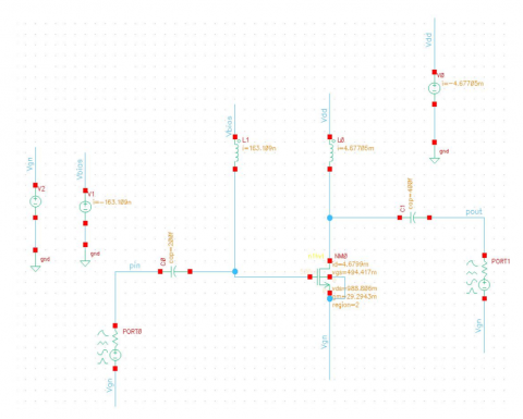
For designing the PA the components are placed as shown in the Figure 9. The signal is applied at Port 0 and the output is terminated at Port 1 with impedance of 50Ω. Initially transient analysis is carried out to check if there is proper amplification.
Figure 8. FinFET transistor parameters after dc biasing
Once it has been verified, the S-parameter analysis has been carried out to check proper matching of input and output at the operating frequency. Parametric analysis has been carried out for varying values of inductors and capacitors in order to achieve proper resonance.
4.2 Simulation results
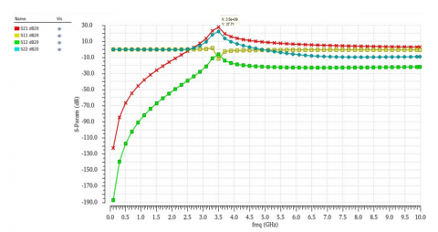
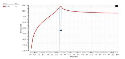
The FinFET single stage amplifier circuit exhibits the anticipated response to the applied RF signal. A 27.71dB gain is attained at the 3.5GHz center frequency. FinFET is a viable contender for 5G communication in the Sub-6 GHz frequency band, according to Figure 10's S-parameter curves. Based on what the simulator recorded, the power gain is 25dB and the obtained bandwidth is 208MHz. Proper matching of the S11, S21, S12, and S22 curves at 3.5GHz is demonstrated by the S-parameter curve plotted using the s-p analysis displayed in Figure 10. This guarantees optimal power transfer by matching the input and output impedance properly. The periodic steady state analysis is performed using the -3dB bandwidth that is computed from Figure 11. The output power is 4.3mW which is approximately equal to 6.335 dBm applying the formula:
$P_{(d B m)}=10 \log _{10}\left(P_{(m W)} / 1 \mathrm{~mW}\right)$ (53)
Figure 9. Simulation set up on Cadence Virtuoso
Table 3. Comparative analysis of the recent work in the area of designing RF PA in mmW and Sub-6 GHz frequency range
|
Reference |
Frequency Band (GHz) |
Topology |
Technology |
Gain (dB) |
Power Gain (dB) |
Bandwidth (MHz) |
Pout (dBm) |
VDD (V) |
|
[27] |
6 - 48 |
Two stages |
22nm FDSOI |
16.8 |
- |
42 |
13 |
2.2 |
|
[28] |
2.4 |
Doherty |
200nm CMOS |
- |
17.2 |
- |
23.2 |
3 |
|
[29] |
0.6 - 6 |
Switchable transformer |
14nm FinFET |
- |
- |
- |
6.5 |
1/1.8 |
|
[30] |
24.5 – 29.5 |
Differential three stack |
28nm CMOS FDSOI |
15 |
- |
- |
19.5 |
3 |
|
[31] |
26 - 30 |
2 stage Doherty PA |
150nm CMOS |
15.7 |
- |
14.6 |
36.1 - 36.5 |
24 |
|
This work |
3.5 |
Single stage |
18nm FinFET |
27.71 |
25 |
208 |
6.33 |
1 |
Figure 10. S-parameter curve obtained from Virtuoso
Figure 11. Bandwidth
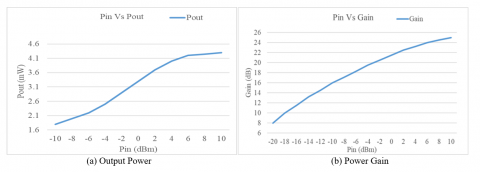
Figure 12. (a) Pin vs. Pout; (b) Pin vs. Power Gain
Plotting the power gain at Psat with a pin in the range of -20dBm to 10dBm reveals the linearity of the steady state analysis and the power gain of 25dB at Psat as shown in Figure 12. Even with switchable transformers in the circuit, the estimated chip area required for Yamaguchi et al. [31] is 3.5 mm2, whereas that Jung et al. [29] founded is 1.92 mm2. This indicates a significant reduction in die area when transitioning to the 14nm FinFET technology. The design offered in this study has the added benefit of not requiring any transformers, which take up a lot of space, and produces output power that is roughly equal to that of Jung et al.’s study [29]. Additionally, the inductor values are much smaller when compared to CMOS technology, which further lowers the needed area. It is thus assumed that the design presented here will require lesser die area. However, another concept explained by Moraes et al. [32] that reduction in area is not always the result of a lower fin count, increase in width and height may become necessary if the routability becomes problematic. Since it is possible to simulate only the components available in the library of Cadence, it is not possible to optimize the FinFET beyond a certain limit. With these limitations too, it was possible to obtain best results in terms of operating frequency, gain, bandwidth and output power at a supply voltage as low as 1V. In comparison to the CMOS technology, and various topologies referred in Table 3, FinFET results are quite encouraging in designing a PA with minimum chip area.
FinFET based PA has provided very promising results in terms of the 3.5GHz operating frequency of the Sub-6 GHz frequency range which is the frequency used in the recent 5G enabled mobile handsets. A high gain of 27.71dB at the operating frequency is much above the required 23dB. The output power is 6.33dBm when configured in a single stage topology and is only slightly lesser than the PA designed using 14nm FinFet Technology which employs a switchable transformer. The proposed design works at a single supply voltage of 1V in comparison with the two voltage levels of the design in Jung et al.’s study [29]. The potential application and benefits lie in the low supply voltage and low chip area. The objective of this work was to design a simplest form of PA with minimum chip area requirements and adaptable to the 5G specifications, which has been successful.
This work opens the door for further research in this area. The FinFET model optimization to provide maximum drain current at the device level can improve the results further. This can be done by modelling the FinFET using TCAD by making structural changes to the fin and gate as discussed by Ghai et al. [33]. If we take into account different topologies for power improvement, such as the Class AB or cascode PA, these results could be further enhanced. Another very important aspect of improving PAE can be by employing efficiency enhancement techniques of which envelope tracking method will be further examined.
|
RF |
Radio Frequency |
|
PA |
Power Amplifier |
|
PAE dB |
Power Added Efficiency decibel |
|
dBm |
decibel-milliwatts |
|
fT |
Cut-off frequency |
|
gm |
transconductance |
|
C |
Capacitance |
|
R |
Resistance |
|
Y |
Signal parameters |
|
Im |
Imaginary |
|
Re |
Real |
|
V |
Voltage |
|
I |
Current |
|
L |
Inductor |
|
H |
Height |
|
W |
Width |
|
P |
Power |
|
S |
Steady State |
|
K |
Small signal Constant |
|
Greek symbols |
|
|
µ |
micro |
|
ω |
angular frequency |
|
τ |
time constant |
|
Subscripts |
|
|
gs |
gate source |
|
ds |
drain source |
|
bias |
bias |
|
dd |
supply voltage |
|
fin |
Fin |
[1] Juneja, S., Pratap, R., Sharma, R. (2021). Semiconductor technologies for 5G implementation at millimeter wave frequencies - Design challenges and current state of work. Engineering Science and Technology, 24(1): 205-217. https://doi.org/10.1016/j.jestch.2020.06.012
[2] Park, B., Kim, J., Cho, Y., Jin, S., Kang, D., Kim, B. (2014). CMOS linear power amplifier with envelope tracking operation (Invited Paper). Journal of Electromagnetic Engineering and Science, 14(1): 1-8. https://doi.org/10.5515/jkiees.2014.14.1.1
[3] Mukai, K., Okabe, H., Tanaka, S. (2021). Recent Progress in Envelope Tracking Power Amplifiers for Mobile Handset Systems. IEICE Transactions on Electronics, E104.C(10): 516-525. https://doi.org/10.1587/transele.2021mmi0005
[4] Alsahali, S., Gecan, D., Alt, A., Chen, P., Woodington, S., Sheikh, A., Sheikh, P., Lees, J. (2020). Modulated rapid load pull system for the emulation of envelope tracking power amplifiers. Electronics Letters, 56(7): 325-328. https://doi.org/10.1049/el.2019.3896
[5] Daneshgar, S., Dasgupta, K., Thakkar, C., Chakrabarti, A., Levy, C.S., Jaussi, J.E., Casper, B. (2020). High-power generation for mm-wave 5G power amplifiers in deep submicrometer planar and FinFET bulk CMOS. IEEE Transactions on Microwave Theory and Techniques, 68(6): 2041-2056. https://doi.org/10.1109/TMTT.2020.2990638
[6] Hamidi, S.B., Dawn, D. (2021). Fully integrated CMOS tunable power amplifier using reconfigurable input/interstage/output matching networks. Analog Integrated Circuits and Signal Processing, 107(1): 73-82. https://doi.org/10.1007/s10470-020-01777-9
[7] Hassan, M., Larson, L.E., Leung, V.W., Asbeck, P.M. (2012). A Combined series-parallel hybrid envelope amplifier for envelope tracking mobile terminal rf power amplifier applications. IEEE Journal of Solid-State Circuits, 47(5): 1185-1198. https://doi.org/10.1109/JSSC.2012.2184639
[8] Mukku, P.K., Naidu, S., Mokara, D., Pydi Reddy, P., Sunil Kumar, K. (2020). Recent trends and challenges on low-power FinFET devices. Smart Innovation, Systems and Technologies, 160: 499-510. https://doi.org/10.1007/978-981-32-9690-9_55
[9] Wambacq, P., Verbruggen, B., Scheir, K., et al. (2007). The potential of FinFETs for analog and RF circuit applications. IEEE Transactions on Circuits and Systems I: Regular Papers, 54(11): 2541-2551. https://doi.org/10.1109/TCSI.2007.907866
[10] Hassanzadeh, A., Hadidi, S. (2021). Systematic approach for IG-FinFET amplifier design using gm/Id method. Analog Integrated Circuits and Signal Processing, 109(2): 379-385. https://doi.org/10.1007/s10470-021-01917-9
[11] Singh, J., Ciavatti, J., Sundaram, K., et al. (2017). 14-nm FinFET technology for analog and RF applications. IEEE Transactions on electron devices, 65(1): 31-37. https://doi.org/10.1109/TED.2017.2776838
[12] Claeys, C., Simoen, E. (2019). Advanced CMOS integration technologies for future mobile applications. In SBMicro 2019 - 34th Symposium on Microelectronics Technology and Devices, Sao Paulo, Brazil, pp. 1-7. https://doi.org/10.1109/SBMicro.2019.8919478
[13] Rajak, A. (2014). A Survey on FinFETs: Technology, pros, cons and improvement prospects. International Journal of Advanced Technology in Engineering and Science, 2: 229-237.
[14] Dančak, C. (2018). The FinFET: A tutorial. Semiconductor Nanotechnology: Advances in Information and Energy Processing and Storage, Springer, Cham, pp. 37-69. https://doi.org/10.1007/978-3-319-91896-9_2
[15] Kushwah, R.S., Akashe, S. (2013). FinFET based tunable analog Circuit: Design and analysis at 45 nm technology. Chinese Journal of Engineering, 2013: 1-8. https://doi.org/10.1155/2013/165945
[16] Mariappan, S., Rajendran, J., Noh, N.M., Ramiah, H., Manaf, A.A. (2020). Energy efficiency in CMOS power amplifier designs for ultralow power mobile wireless communication systems. Turkish Journal of Electrical Engineering and Computer Sciences, 28(1): 1-16. https://doi.org/10.3906/elk-1903-47
[17] Bhuiyan, M.A.S., Badal, M.T.I., Reaz, M.B.I., Crespo, M.L., Cicuttin, A. (2019). Design architectures of the CMOS power amplifier for 2.4 GHz ISM band applications: An overview. Electronics, 8(5): 477. https://doi.org/10.3390/electronics8050477
[18] Bameri, H., Hakimi, A., Movahhedi, M. (2011). A linear-high range output power control technique for cascode power amplifiers. Microelectronics Journal, 42(9): 1025-1031. https://doi.org/10.1016/j.mejo.2011.07.002
[19] Koo, B., Na, Y., Hong, S. (2012). Integrated bias circuits of RF CMOS cascode power amplifier for linearity enhancement. IEEE Transactions on Microwave Theory and Techniques, 60(2): 340-351. https://doi.org/10.1109/TMTT.2011.2177857
[20] Rahati Belabad, A., Masoumi, N., Ashtiani, S.J. (2013). A fully integrated 2.4GHz CMOS high power amplifier using parallel class A&B power amplifier and power-combining transformer for WiMAX application. AEU - International Journal of Electronics and Communications, 67(12): 1030-1037. https://doi.org/10.1016/j.aeue.2013.06.004
[21] Lee, C.I., Lin, W.C., Lin, Y.T. (2014). A 2.4 GHz high output power and high efficiency power amplifier operating at inductive breakdown in CMOS technology. Microelectronics Journal, 45(4): 449-453. https://doi.org/10.1016/j.mejo.2014.02.008
[22] Jeon, H., Lee, K.S., Lee, O., et al. (2013). A cascode feedback bias technique for linear CMOS power amplifiers in a multistage cascode topology. IEEE Transactions on Microwave Theory and Techniques, 61(2): 890-901. https://doi.org/10.1109/TMTT.2012.2235456
[23] Kayyil, A.V., Qiao, B., Allstot, D.J. (2021). Linearity improvement techniques for CMOS switched-capacitor power amplifiers. In 2021 IEEE International Symposium on Circuits and Systems (ISCAS), Daegu, Korea, pp. 1-5. https://doi.org/10.1109/ISCAS51556.2021.9401494
[24] Qin, M., Sun, Y., Li, X., Shi, Y. (2018). Analytical parameter extraction for small-signal equivalent circuit of 3D FinFET into Sub-THz range. IEEE Access, 6: 19752-19761. https://doi.org/10.1109/ACCESS.2018.2822672
[25] Kang, I.M., Shin, H. (2006). Non-quasi-static small-signal modeling and analytical parameter extraction of SOI FinFETs. IEEE Transactions on Nanotechnology, 5(3): 205-210. https://doi.org/10.1109/TNANO.2006.869946
[26] Ellinger, F. (2008). Radio Frequency Integrated Circuits and Technologies. Springer Science & Business Media. https://doi.org/10.1007/978-3-540-35790-2
[27] Le, Q.H., Huynh, D.K., Nayak, A., Kämpfe, T., Rudolph, M. (2022). A Performance Study of 22nm FDSOI CMOS for Wideband 5G Power Amplifier Applications. In 2022 14th German Microwave Conference (GeMiC), Ulm, Germany, pp. 61-64.
[28] Barmala, E. (2019). Design and simulate a Doherty power amplifier using GaAs technology for telecommunication applications. Indonesian Journal of Electrical Engineering and Computer Science, 15(2): 845-854. https://doi.org/10.11591/ijeecs.v15.i2.pp845-854
[29] Jung, W., Kang, S., Jeong, D., Son, K.Y., Lee, J., Lee, J., Paek, J.S. (2021). A Sub-6GHz 5G New Radio Multi-Band Transmitter with a Switchable Transformer in 14nm FinFET CMOS. In 2021 IEEE Radio Frequency Integrated Circuits Symposium (RFIC), Atlanta, GA, USA, pp. 163-166. https://doi.org/10.1109/RFIC51843.2021.9490416
[30] Bhagavatula, V., Zhang, F., Kuo, C., et al. (2022). A 5G FR2 power-amplifier with an integrated power-detector for closed-loop EIRP control. IEEE Journal of Solid-State Circuits, 57(5): 1257-1266. https://doi.org/10.1109/JSSC.2022.3146872
[31] Yamaguchi, Y., Nakatani, K., Shinjo, S. (2020). A wideband and high efficiency Ka-band GaN Doherty power amplifier for 5G communications. In 2020 IEEE BiCMOS and Compound Semiconductor Integrated Circuits and Technology Symposium (BCICTS), Monterey, CA, USA, pp. 1-4. https://doi.org/10.1109/BCICTS48439.2020.9392982
[32] Moraes, L.B., Zimpeck, A.L., Meinhardt, C., Reis, R. (2020). Robust FinFET Schmitt trigger designs for low power applications. In VLSI-SoC: New Technology Enabler: 27th IFIP WG 10.5/IEEE International Conference on Very Large Scale Integration, VLSI-SoC 2019, Cusco, Peru, pp. 45-68. https://doi.org/10.1007/978-3-030-53273-4
[33] Ghai, D., Mohanty, S.P., Thakral, G. (2013). Comparative analysis of double gate FinFET configurations for analog circuit design. In 2013 IEEE 56th International Midwest Symposium on Circuits and Systems (MWSCAS), Columbus, OH, USA, pp. 809-812. https://doi.org/10.1109/MWSCAS.2013.6674772