M. R. D. Al-Mothafar![]()
© 2023 IIETA. This article is published by IIETA and is licensed under the CC BY 4.0 license (http://creativecommons.org/licenses/by/4.0/).
OPEN ACCESS
This study investigates the application of peak current-mode control to a dual-module, independent-input, series-output boost DC-DC converter characterized by mismatched inductors. The converter, operating in continuous-conduction mode, incorporates non-identical modules, each supplied by a distinct voltage source while their outputs are interconnected in series. A small-signal state-space averaged model, useful for individual module control, is proposed. Utilizing this model, both direct and cross-coupling control-to-output voltage small-signal responses under inductor mismatch are generated with MATLAB assistance. A conventional Type-2 Proportional-Integral controller is designed for the module voltage loop, guided by the direct control-to-output voltage responses. The impact of inductor mismatch on the transient performance of the module input current and output voltage under step changes in the load current and module source voltage is examined. The cycle-by-cycle simulations conducted via PSIM demonstrate significant agreement with the model predictions.
small-signal modelling, current-mode control, state-space averaged model, independent-input series-output, modular boost DC-DC converter, inductor mismatch
Modular DC-DC power conversion architectures, which incorporate two or more individual modules in various series/parallel configurations, have been demonstrated to provide efficient and reliable solutions for a range of applications, including renewable energy systems, distributed power systems, and specialized switched-mode DC power supplies. Four fundamental connection arrangements for modular DC-DC converters have been extensively studied in existing literature: parallel-input/parallel-output (PIPO) [1-4], parallel-input/series-output (PISO) [5-9], series-input/parallel-output (SIPO) [10-18], and series-input/series-output (SISO) [12, 14, 19, 20]. These studies [1-20] offer a snapshot of recent publications on these four fundamental arrangements, which also serve as a gateway to earlier works. Besides these configurations, more advanced modular structures have been explored, such as independent-input/parallel-output (IIPO) [21-26], independent-input/series-output (IISO) [27-36], and series-input/independent-output (SIIO) [37]. Research has also extended to more complex configurations, such as series-parallel-input/series-output [38], series-input/series-parallel-output [39], and series-parallel-input/series-parallel-output [40].
Various control methods have been proposed for the regulation of modular DC-DC converters, and many of these methods have been classified and reviewed in studies [41, 42]. One method, known as peak current-mode control (PCMC), is favored by many researchers due to its established advantages including fast response, stable current sharing, and precise output voltage regulation [42]. This control technique has been applied to PIPO [1, 3], PISO [8], SIPO [10], SISO [12], IIPO [24, 26], IISO [35, 36], and SIIO [37] converters. Preliminary analysis of the dynamics of PCMC converters is typically performed using linearized small-signal (SS) models. Deriving these models becomes straightforward when the modular converter can be replaced by an equivalent single module. However, in instances where the converter is powered from independent sources, such as those employing the IISO and IIPO structures, or when a parametric mismatch exists between the converter’s constituent modules, a reduced-order model may not be feasible. In such cases, detailed SS models are required.
The primary aim of this research is to devise a SS model that can be used for the design of voltage feedback controllers in the presence of inductor mismatch for an IISO PCMC boost converter. A converter with the IISO structure is powered from separate energy sources, achieving higher output voltages by series-connecting the outputs from two or more single-cell converters. Over the past three decades, numerous studies have been published on IISO converters for various applications, particularly focusing on renewable and distributed energy systems, and high-voltage DC power supplies [27-36]. While various control methodologies have been utilized, only two works [35, 36] have implemented PCMC. However, in these studies, the current-mode control SS analysis has only been conducted for the case of identical modules. To date, no published work has reported a state-space SS model for an IISO boost converter comprising non-identical modules nor investigated the impact of mismatch in inductance values on the control of this converter. It will be demonstrated in the following sections that this mismatch influences the location of the module right-half-plane zero, thereby impacting the design of the voltage feedback loop controller.
The contributions of this work are threefold:
(1) A small-signal model is developed for a PCMC IISO boost DC-DC converter consisting of two non-identical modules.
(2) Direct and cross-coupling control-to-output voltage frequency responses of the converter are generated and studied in the presence of inductor mismatch.
(3) Voltage feedback loop controllers for the mismatched modules are designed, and closed-loop transient responses are produced and studied under step changes in the load current and module input voltage.
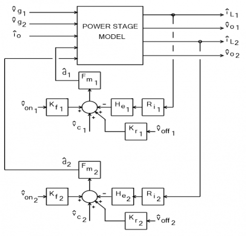
The converter schematic is depicted in Figure 1 where two separately-fed and independently-controlled PCMC boost cells working in the continuous-conduction mode are connected in series at their outputs to supply the load. A voltage attenuator $K_v$ and a type-2 controller represented by $F_v$ are used in each voltage feedback loop.
Figure 1. Representation of the two-module IISO converter
The PCMC of the individual module resembles that of the single boost converter. Transistor ON time and switching cycle T is initiated by a constant-frequency clock. Sensed inductor current which has a rising slope (Sn=Ri*Vg/L) is compared to control voltage Vc and an external ramp slope Se. The comparison result determines the transistor duty ratio D. The external ramp is used to ensure stability of the current loop when D is greater than 0.5 [43].
In order to design the module voltage feedback loop controller under inductor mismatch, a SS model is established. The model takes into account the sampling effect of the current loops and is suitable to use up to half the switching frequency.
The module PCMC stage is modelled using a modified “new continuous-time technique” [43, 44]. The PCMC-stage law of each of the mismatched modules is augmented with the power-stage state-space equations to allow generating the direct and cross-coupling control-to-output voltage SS responses under inductor mismatch conditions. The module voltage-loop controller is designed based on the direct control-to-output voltage frequency response when the inductance has its maximum value. Closed-loop time-domain responses under step changes in the load current and module input voltage are produced using MATLAB/SIMULINK to assess the effect of inductor mismatch.
For an assumed mismatch of ±25% between inductor values, the major findings of this study are: the mismatch causes small changes to the overshoot/undershoot values of the module inductor current and output voltage closed-loop transient responses; the change in power losses due to inductor-current ripple mismatch is insignificant; and the dc load voltage remains equally distributed between the two modules. The entire model predicted responses correlate well with PSIM cycle-by-cycle simulations.
Small-signal models are useful tools for the initial investigation of the dynamics of complex interconnected converter systems and also for feedback control design.
2.1 Power stage
Assuming ideal components, the SS model of the power stage can be characterized [36] by:
$\dot{\hat{x}}=\frac{d}{d t}\left[\begin{array}{c}\hat{\imath}_{L 1} \\ \hat{v}_{o 1} \\ \hat{\imath}_{L 2} \\ \hat{v}_{o 2}\end{array}\right]=[A]\left[\begin{array}{c}\hat{\imath}_{L 1} \\ \hat{v}_{o 1} \\ \hat{\imath}_{L 2} \\ \hat{v}_{o 2}\end{array}\right]+[B]\left[\begin{array}{c}\hat{d}_1 \\ \hat{d}_2 \\ \hat{v}_{g 1} \\ \hat{v}_{g 2} \\ \hat{\imath}_o\end{array}\right]$ (1a)
where,
$[A]=\left[\begin{array}{cccc}0 & \frac{-D_1^{\prime}}{L_1} & 0 & 0 \\ \frac{D_1^{\prime}}{C_1} & \frac{-1}{R C_1} & 0 & \frac{-1}{R C_1} \\ 0 & 0 & 0 & \frac{-D_2^{\prime}}{L_2} \\ 0 & \frac{-1}{R C_2} & \frac{D_2^{\prime}}{C_2} & \frac{-1}{R C_2}\end{array}\right]$ (1b)
$[B]=\left[\begin{array}{ccccc}\frac{V_{g 1}}{D_1^{\prime} L_1} & 0 & \frac{1}{L_1} & 0 & 0 \\ \frac{-2 V_{g 1}}{D_1^{\prime 2} R C_1} & 0 & 0 & 0 & \frac{1}{C_1} \\ 0 & \frac{V_{g 2}}{D_2^{\prime} L_2} & 0 & \frac{1}{L_2} & 0 \\ 0 & \frac{-2 V_{g 2}}{D_2^{\prime 2} R C_2} & 0 & 0 & \frac{1}{C_2}\end{array}\right]$ (1c)
The symbol (^) denotes SS changes and $D^{\prime}=1-D$.
2.2 PCMC stage
The module PCMC stage can be modelled in a way similar to that of the single-stage boost cell [43]. The SS model is illustrated in Figure 2 and consists of:
Table 1. Small-signal model parameters
|
Modulator Gain |
$\begin{aligned} F_{m 1}= & \frac{1}{\left(S_{n 1}+S_{e 1}\right) T}=\frac{L_1}{M_{c 1} R_{i 1} V_{g 1} T} \\ F_{m 2}= & \frac{1}{\left(S_{n 2}+S_{e 2}\right) T}=\frac{L_2}{M_{c 2} R_{i 2} V_{g 2} T} \\ & \text { where } M_{c 1}=1+s_{e 1} / s_{n 1} \\ & \text { and } M_{c 2}=1+s_{e 2} / s_{n 2}\end{aligned}$ |
|
Sampling Gain |
$H_{e 1}=H_{e 2} \cong\left(1+\frac{s}{\omega_n Q_z}+\frac{s^2}{\omega_n^2}\right)$ where $Q_z=-2 / \pi$ and $\omega_n=\pi / T$ |
|
Feedforward Gain of Input Voltage |
$\begin{aligned} & K_{f 1}=\frac{-D_1 T R_{i 1}\left(1-0.5 D_1\right)}{L_1}+\frac{D_1^2 T^2 R_{i 1}\left(3-2 D_1\right)}{12 L_1} s \\ & K_{f 2}=\frac{-D_2 T R_{i 2}\left(1-0.5 D_2\right)}{L_2}+\frac{D_2^2 T^2 R_{i 2}\left(3-2 D_2\right)}{12 L_2} s\end{aligned}$ |
|
Feedforward Gain of Output Voltage |
$\begin{aligned} & K_{r 1}=\frac{\left(1-D_1\right)^2 T R_{i 1}}{2 L_1} \\ & K_{r 2}=\frac{\left(1-D_2\right)^2 T R_{i 2}}{2 L_2}\end{aligned}$ |
|
Inductor Voltage During the ON and OFF Times |
$\begin{aligned} & \hat{v}_{o n 1}=\hat{v}_{g 1} ; \hat{v}_{o f f 1}=\hat{v}_{o 1}-\hat{v}_{g 1} \\ & \hat{v}_{o n 2}=\hat{v}_{g 2} ; \hat{v}_{o f f 2}=\hat{v}_{o 2}-\hat{v}_{g 2}\end{aligned}$ |
Using Figure 2, the duty ratio laws can be expressed as:
$\hat{d}_1=F_{m 1}\left(\hat{v}_{c 1}-R_{i 1} H_{e 1} \hat{\imath}_{L 1}+K_{f 1} \hat{v}_{o n 1}+K_{r 1} \hat{v}_{o f f 1}\right)$ (2a)
$\hat{d}_2=F_{m 2}\left(\hat{v}_{c 2}-R_{i 2} H_{e 2} \hat{\imath}_{L 2}+K_{f 2} \hat{v}_{o n 2}+K_{r 2} \hat{v}_{o f f 2}\right)$ (2b)
Figure 2. Small-signal model with only current loops closed
After the application of Laplace transforms to (1) and the substitution for the duty ratios from (2), we can write:
$\begin{aligned} & {\left[\begin{array}{c}s \hat{\imath}_{L 1} \\ s \hat{v}_{o 1} \\ s \hat{\imath}_{L 2} \\ s \hat{v}_{o 2}\end{array}\right]=\left[\begin{array}{cccc}A_{11} & A_{12} & 0 & 0 \\ A_{21} & A_{22} & 0 & A_{24} \\ 0 & 0 & A_{33} & A_{34} \\ 0 & A_{42} & A_{43} & A_{44}\end{array}\right]\left[\begin{array}{c}\hat{\imath}_{L 1} \\ \hat{v}_{o 1} \\ \hat{\imath}_{L 2} \\ \hat{v}_{o 2}\end{array}\right]} +\left[\begin{array}{ccccc}B_{11} & 0 & B_{13} & 0 & 0 \\ B_{21} & 0 & B_{23} & 0 & B_{25} \\ 0 & B_{32} & 0 & B_{34} & 0 \\ 0 & B_{42} & 0 & B_{44} & B_{45}\end{array}\right]\left[\begin{array}{c}\hat{v}_{c 1} \\ \hat{v}_{c 2} \\ \hat{v}_{g 1} \\ \hat{v}_{g 2} \\ \hat{\imath}_0\end{array}\right]\end{aligned}$ (3)
The $A$ and $B$ elements of (3) are presented in Table 2, and the parameters $F_m, H_e, K_r$ and $K_f$ are as given in Table 1 .
In summary, augmenting the power-stage SS model with the PCMC law of each module produced Eq. (3) which characterizes the converter model with closed current loops. By using (3) the SS transfer function expressions of an IISO PCMC boost converter consisting of two non-identical modules can be found.
Table 2. Elements of Eq. (3)
|
A11 |
$\frac{-V_{O 1} R_{i 1} H_e F_{m 1}}{L_1}$ |
B11 |
$\frac{V_{o 1} F_{m 1}}{L_1}$ |
|
A12 |
$\frac{-D_1^{\prime}+V_{o 1} F_{m 1} K_{r 1}}{L_1}$ |
B13 |
$\frac{1+V_{o 1} F_{m 1}\left(K_{f 1}-K_{r_1}\right)}{L_1}$ |
|
A21 |
$\frac{D_1^{\prime}+I_{L 1} R_{i 1} H_e F_{m 1}}{C_1}$ |
B21 |
$\frac{-I_{L 1} F_{m 1}}{C_1}$ |
|
A22 |
$\frac{-1}{C_1}\left(\frac{1}{R}+I_{L 1} F_{m 1} K_{r 1}\right)$ |
B23 |
$\frac{-I_{L 1} F_{m 1}\left(K_{f 1}-K_{r 1}\right)}{C_1}$ |
|
A24 |
$\frac{-1}{R C_1}$ |
B25 |
$\frac{1}{C_1}$ |
|
A33 |
$\frac{-V_{o 2} R_{i 2} H_e F_{m 2}}{L_2}$ |
B32 |
$\frac{V_{o 2} F_{m 2}}{L_2}$ |
|
A34 |
$\frac{-D_2^{\prime}+V_{o 2} F_{m 2} K_{r 2}}{L_2}$ |
B34 |
$\frac{1+V_{o 2} F_{m 2}\left(K_{f 2}-K_{r 2}\right)}{L_2}$ |
|
A42 |
$\frac{-1}{R C_2}$ |
B42 |
$\frac{-I_{L 2} F_{m 2}}{C_2}$ |
|
A43 |
$\frac{D_2^{\prime}+I_{L 2} R_{i 2} H_e F_{m 2}}{C_2}$ |
B44 |
$\frac{-I_{L 2} F_{m 2}\left(K_{f 2}-K_{r_2}\right)}{C_2}$ |
|
A44 |
$\frac{-1}{C_2}\left(\frac{1}{R}+I_{L 2} F_{m 2} K_{r 2}\right)$ |
B45 |
$\frac{1}{C_2}$ |
The direct and cross-coupling control-to-output voltage SS transfers denoted by $\left(\hat{v}_{o 1} / \hat{v}_{c 1}\right)$ and $\left(\hat{v}_{o 2} / \hat{v}_{c 1}\right)$ respectively are obtained from Eq. (3) and programmed into MATLAB software using the parameters:
$\begin{gathered}V_{g 1}=V_{g 2}=24 \mathrm{~V} ; V_{o 1}=V_{o 2}=96 \mathrm{~V} ; R=64 \Omega ; T=10 \mu \mathrm{s} ; \\ C_1=C_2=24 \mu \mathrm{F} ; R_{i 1}=R_{i 2}=0.1 \Omega ; \\ L_1=100 \mu \mathrm{H} \pm 25 \% ; L_2=100 \mu \mathrm{H}\end{gathered}$
Three cases of inductance values are considered:
A mismatch of ±25% is chosen because the tolerance in inductance values can typically vary from several percent up to 15% according to the study [45], and gets worse in time due to aging.
MATLAB generated Bode plots of $\left(\hat{v}_{o 1} / \hat{v}_{c 1}\right)$ and $\left(\hat{v}_{o 2} / \hat{v}_{c 1}\right)$ are compared with PSIM “ac sweep” results. The “ac sweep” command is enabled after implementing the IISO converter of Figure 1 with voltage feedback loops left open.
Figure 3 shows the model predictions of $\left(\hat{v}_{o 1} / \hat{v}_{c 1}\right)$ responses for the three cases mentioned above with external ramp amplitude $V_{\text {ramp }}$=0.34 V, while Figure 4 gives the responses with $V_{\text {ramp }}$=0.86 V. The ramp values are selected to inspect the under-damped and damped responses. These figures also show the results found using PSIM “ac sweep”. It can be seen that PSIM results correlate well with those predicted by the proposed model up to ½ the switching frequency region. Figures 3 and 4 show that the low-frequency responses (up to≈900 Hz) are slightly affected by the ±25% mismatch in inductance values. A more noticeable change can be seen as frequency increases. The zero-pole locations of $\left(\hat{v}_{o 1} / \hat{v}_{c 1}\right)$ predicted by MATLAB are given in Table 3 which shows that when $V_{\text {ramp }}$=0.34 V, the low-frequency response is influenced by a real right-half s-plane (RHSP) zero, and two real left-half s-plane (LHSP) poles sandwiching a real zero. At half the switching frequency, a complex pair of poles appears because of the current-loop sampling action, and hence the peaking observed in Figure 3. Similar to the single-cell PCMC boost converters, this peaking can be reduced or eliminated by increasing the slope ratio $S_e / S_n$. For the selected parameters and the nominal value of inductances (i.e., $L_1$=$L_2$=100 µH) critical damping is achieved with $V_{\text {ramp }}$≈0.86 V which is equivalent to slope ratio $S_e / S_n$=3.6.
Table 3 also shows that the RHSP zero of $\left(\hat{v}_{o 1} / \hat{v}_{c 1}\right)$ moves to lower frequencies as inductance is increased (more on this in Section 4). The location of this zero can be expressed as:
$\omega_{r h s p z}=R(1-D)^2 /\left(2 L_1\right)$ (4)
Figure 3. Direct control-to-output voltage (Vramp=0.34 V): Top Bode plots: model prediction; Bottom plots: PSIM
Figure 4. Direct control-to-output voltage (Vramp=0.86 V): Top Bode plots: model prediction; Bottom plots: PSIM
Figures 5 and 6 show the responses of the cross-coupling control-to-output voltage $\left(\hat{v}_{o 2} / \hat{v}_{c 1}\right)$ when Vramp=0.34 V and Vramp=0.86 V respectively, while Table 4 gives the corresponding zero-pole locations. $\left(\hat{v}_{o 2} / \hat{v}_{c 1}\right)$ has the same poles and RHSP zero observed in the direct transfer function $\left(\hat{v}_{o 1} / \hat{v}_{c 1}\right)$ but the low-frequency LHSP zero is absent. The response of $\left(\hat{v}_{o 2} / \hat{v}_{c 1}\right)$ is affected by the external ramp in a similar fashion. Also, the effect of inductance mismatch on $\left(\hat{v}_{o 2} / \hat{v}_{c 1}\right)$ resembles that observed with $\left(\hat{v}_{o 1} / \hat{v}_{c 1}\right)$ in the sense that it causes slight changes in the magnitude and phase responses at low frequencies.
Table 3. Direct control-to-output voltage pole-zero locations in (rad/sec)
|
|
Vramp=0.34 V |
Vramp=0.86 V |
||||
|
|
L1=L2=100 µH |
L1=75 µH L2=100 µH |
L1=125 µH L2=100 µH |
L1=L2= 100 µH |
L1=75 µH L2=100 µH |
L1=125 µH L2=100 µH |
|
Zeros |
-45298+3.0613e+05i -45298-3.0613e+05i -2090 20000 |
-45298+3.0613e+05i -45298-3.0613e+05i -2090 26667 |
-45298+3.0613e+05i -45298-3.0613e+05i -2090 16000 |
-3.8164e+05 -2.5909e+05 -2254.5 20000 |
-3.8164e+05 -2.5909e+05 -2254.5 26667 |
-3.8164e+05 -2.5909e+05 -2254.5 16000 |
|
Poles |
-45296+3.0613e+05i -45296-3.0613e+05i -45300+3.0613e+05i -45300-3.0613e+05i -2745.2 -1434.8 |
-45298+3.0613e+05i -45298-3.0613e+05i -9497.3+3.0937e+05i -9497.3-3.0937e+05i -2751.4 -1441.7 |
-45298+3.0613e+05i -45298-3.0613e+05i -87240+2.9706e+05i -87240-2.9706e+05i -2743.7 -1432.5 |
-3.8166e+05 -3.8162e+05 -2.5906e+05 -2.5912e+05 -1593.3 -2915.8 |
-2.0347e+05+2.3533e+05i -2.0347e+05-2.3533e+05i -3.8164e+05 -2.5909e+05 -1595.9 -2916 |
-3.8164e+05 -7.6548e+05 -2.5909e+05 -1.34e+05 -1592.8 -2918 |
Figure 5. Cross-coupling control-to-output voltage (Vramp=0.34 V): Top Bode plots: model prediction; Bottom plots: PSIM
Figure 6. Cross-coupling control-to-output voltage (Vramp=0.86 V): Top Bode plots: model prediction; Bottom plots: PSIM
Table 4. Cross-coupling control-to-output voltage pole-zero locations in (rad/sec)
|
|
Vramp=0.34 V |
Vramp=0.86 V |
||||
|
|
L1=L2=100 µH |
L1=75 µH L2=100 µH |
L1=125 µH L2=100 µH |
L1=L2=100 µH |
L1=75 µH L2=100 µH |
L1=125 µH L2=100 µH |
|
Zeros |
-45361+3.071e+05i -45361-3.071e+05i 20000 |
-45361+3.071e+05i -45361-3.071e+05i 26667 |
-45361+3.071e+05i -45361-3.071e+05i 16000 |
-3.6807e+05 -2.7276e+05 20000 |
-3.6807e+05 -2.7276e+05 26667 |
-3.6807e+05 -2.7276e+05 16000 |
|
Poles |
-45296+3.0613e+05i -45296-3.0613e+05i -45300+3.0613e+05i -45300-3.0613e+05i -2745.2 -1434.8 |
-45298+3.0613e+05i -45298-3.0613e+05i -9497.3+3.0937e+05i -9497.3-3.0937e+05i -2751.4 -1441.7 |
-45295+3.0607e+05i -45295-3.0607e+05i -87243+2.9713e+05i -87243-2.9713e+05i -2743.6 -1432.3 |
-3.8166e+05 -3.8162e+05 -2.5906e+05 -2.5912e+05 -1593.3 -2915.8 |
2.0347e+05+2.3533e+05i -2.0347e+05-2.3533e+05i -3.8164e+05 -2.5909e+05 -1595.9 -2916 |
-3.8164e+05 -7.6548e+05 -2.5909e+05 -1.34e+05 -1592.8 -2918 |
This section studies the impact of mismatch on the transient behaviour of the module inductor (= input) current and output voltage when all the current and voltage feedback loops are closed. Figure 7 shows the MATLAB/SIMULINK model used for this purpose. The module voltage feedback loop is comprised of an attenuator Kv and a type-2 compensator Fvwhose design is based on the direct control-to-output voltage response when the inductance has its maximum value (i.e., when L=125 μH) with no peaking present at ½ the switching frequency (i.e., with Vramp=0.86 V). The maximum inductance case is chosen as basis for the design in order to ensure system stability. This is so, because the module RHSP zero moves to lower frequencies as the inductance increases. With other parameters of (4) kept unchanged, the RHSP zero locates at≈2.55 kHz when L=125 μH. Traditional compensator design rules for single DC-DC converters [46] are applied; a crossover frequency of 850 Hz (≈ 1/3 of the RHSP zero location), and a phase margin of 60° are chosen as design data for PSIM “smart control” which is a controller-design software for converter circuits. PSIM response of $\left(\hat{v}_{o 1} / \hat{v}_{c 1}\right)$ is exported to “smart control” to get the compensator transfer function according to the mentioned design rules. The expression for the module compensator transfer function is:
$F_{v 1}=F_{v 2}=8804 \frac{(1+s / 1718)}{s(1+s / 16595)}$ (5)
Figure 7. Matlab/Simulink model for generating the time-domain transients
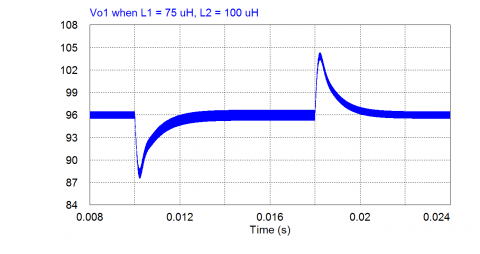
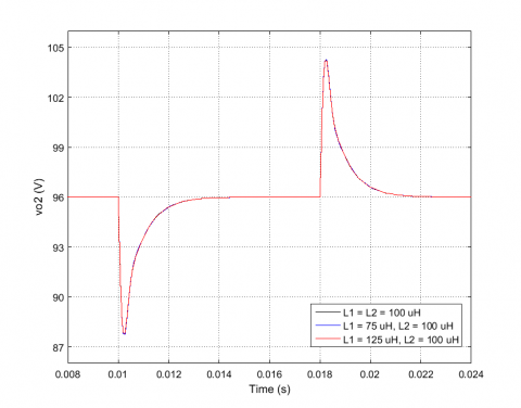
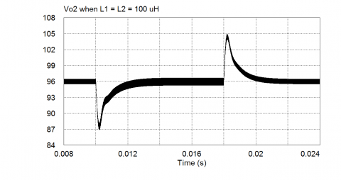
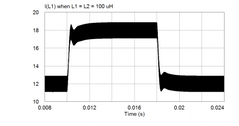
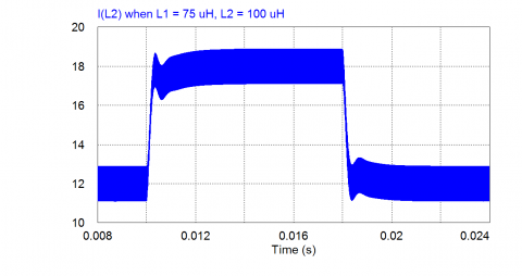
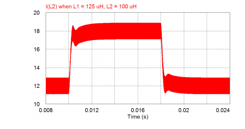
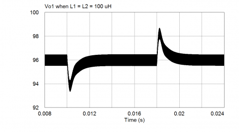
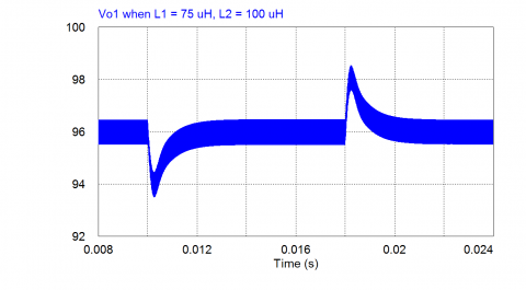
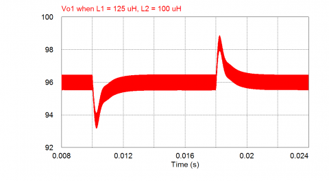
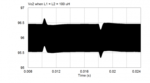
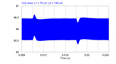
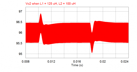
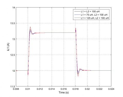
Figures 8 and 9 respectively show the closed-loop output voltage transient responses of modules 1 and 2 under ± 50% step disturbances in load current for the same cases of inductor values: (L1=L2=100 µH), (L1=75 µH, L2=100 µH), and (L1=125 µH, L2=100 µH). Each figure shows the predictions of the MATLAB/SIMULINK averaged model and PSIM cycle-by-cycle simulation results. Two step changes are considered: These are from 3 A to 4.5 A at 10 msec and from 4.5 A to 3 A at 18 msec. From Figures 8 and 9 the following can be stated: (a) the effect of inductance mismatch appears only in the output voltage of the module whose inductance value deviates from the nominal value (module 1 in this case); less than 1% change in the overshoot/undershoot values is observed with the mismatch of ±25% in inductance values; (b) the module average output voltage is not affected by the inductor mismatch and is controlled at the required value of 96 V, with a settling time of about 4.5 msec and overshoot/undershoot values of no more than 10% of the dc output voltage.
(a)
(b)
(c)
(d)
Figure 8. Output voltage responses of module 1 due to step disturbances in load current: (a) Model predictions. (b), (c) and (d) PSIM verification
(a)
(b)
(c)
(d)
Figure 9. Output voltage responses of module 2 due to step disturbances in load current: (a) Model predictions. (b), (c) and (d) PSIM verification
(a)
(b)
(c)
(d)
Figure 10. Inductor current responses of module 1 due to step disturbances in load current: (a) Model predictions. (b), (c) and (d) PSIM verification
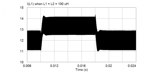
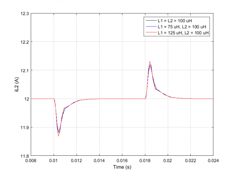
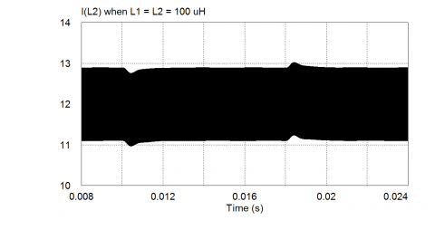
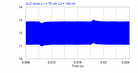
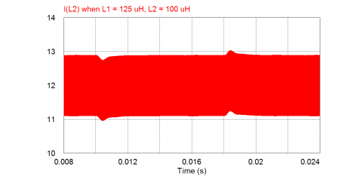
Figures 10 and 11 respectively show the closed-loop inductor current transient responses of modules 1 and 2 under ± 50% step disturbances in load current for the three cases under consideration. From these figures the following can be stated: (a) the effect of inductance mismatch can only be noticed in the behaviour of the current of module 1; MATLAB model predicts an overshoot/undershoot in this current of around 1.2% of the steady-state value when inductance is increased from 100 µH to 125 µH, but settling time is hardly affected; (b) cycle-by-cycle simulation results indicate that the transient and steady-state inductor-current ripple of module 1 are affected by the inductor mismatch; current ripple amplitude drops by≈22.2% as inductance value is increased from 100 µH to 125 µH, and goes up by≈33.3% when inductance value is changed from 100 µH to 75 µH. At steady state this current ripple mismatch will result in different rms values and hence different power losses when circuit resistance non-idealities are taken into consideration. The change in the rms value, however, is very small as predicted by PSIM (less than 0.1% for an inductor mismatch of 25%). It is worth mentioning here that power imbalance between modules can have serious effect on the performance of battery-based energy-storage systems employing the bidirectional type of the IISO converter; because the converter charging and discharging modes are decided by the battery state of charge (SOC). Therefore, a battery management system is necessary to ensure SOC equalization.
(a)
(b)
(c)
(d)
Figure 11. Inductor current responses of module 2 due to step disturbances in load current: (a) Model predictions. (b), (c) and (d) PSIM verification
Figures 12 and 13 respectively show the closed-loop output voltage responses of modules 1 and 2 under ±10% step disturbances in the input voltage of module 1, while Figures 14 and 15 depict the corresponding responses of the inductor currents for the three cases under investigation: (L1=L2=100 µH), (L1=75 µH, L2=100 µH), and (L1=125 µH, L2=100 µH). Unlike the responses in Figures 8 to 11, it can be observed here that the step changes impact both modules even when there is no inductance mismatch. With mismatched inductors the module output voltage experiences a small increase in overshoot/undershoot value as inductance value is increased (less than 1% when inductance is changed from 100 µH to 125 µH). A considerable effect of the mismatch appears in the transient and steady-state inductor current ripple of the disturbed module. The change in ripple amplitude is the same as previously mentioned when the load current is step changed. As for the steady-state output voltage, both modules are regulated at the required 96 V; No effect of inductor mismatched has been observed.
(a)
(b)
(c)
(d)
Figure 12. Module 1 output voltage responses due to step changes in its input voltage: (a) Model predictions. (b), (c) and (d) PSIM verification
(a)
(b)
(c)
(d)
Figure 13. Module 2 output voltage responses to step changes in module 1 input voltage: (a) Model predictions. (b), (c) and (d) PSIM verification
Figure 14 also shows that following to the disturbance at 10 msec, the inductor currents of modules 1 and 2 settles at≈13.3 A and 12 A respectively. Due to this difference, the module 1 will have more power losses than module 2. This rise in the current of the disturbed module is not related to inductor mismatch but to the 10% drop in its input voltage. In all the previous figures, the averaged model predictions correlate well with the cycle-by-cycle simulations.
(a)
(b)
(c)
(d)
Figure 14. Inductor current responses of module 1 resulting from step changes to its input voltage: (a) Model predictions. (b), (c) and (d) PSIM verification
(a)
(b)
(c)
(d)
Figure 15. Module 2 inductor current responses resulting from step changes to module 1 input voltage: (a) Model predictions. (b), (c) and (d) PSIM verification
In this study, the peak current-mode control (PCMC) method is applied to a dual-module, independent-input, series-output boost DC-DC converter, operating in continuous-current mode with mismatched inductors. With the current loops closed and the voltage feedback loops open, the results derived from the mathematical, state-space-based small-signal model, in conjunction with PSIM simulations, suggest that a 25% mismatch between the inductor values of the two modules has insignificant impact on the magnitude and phase of the direct and cross-coupling control-to-output voltage small-signal responses at low frequencies (up to approximately 900 Hz). However, the effect becomes more pronounced as the frequency increases.
A conventional compensator is designed for the module voltage feedback loop control, predicated on the frequency response of the direct control-to-output voltage when the inductance has the maximum value. Upon closing all feedback loops and applying step disturbances to the load current and module input voltage, it is observed that a 25% mismatch in inductor values induces minor deviations, not exceeding 1.2%, in the overshoot/undershoot values of the module inductor current and output voltage.
Despite the 25% mismatch eliciting a relatively large variation in the inductor-current ripple, reaching 33%, the consequent change in power losses due to this inductor-current ripple mismatch is less than 0.1%. Furthermore, the module DC output voltage following the step disturbances remains unaffected by the inductor mismatch, and the load voltage is equally distributed among the constituent modules.
Future research should focus on three main areas: 1) extending the derived small-signal model to account for circuit parasitics; 2) examining the effect of inductor mismatch under varying operating conditions; and 3) exploring alternative control strategies that may enhance the system’s dynamic performance.
[1] Geetha, M.R., Malar, R.S.M., Ahilan, T. (2016). Current sharing in parallel connected boost converters. IET Journal of Engineering, 2016(12): 444-452. https://doi.org/10.1049/joe.2016.0238
[2] Xia, Y., Li, Y., Peng, Y., Yu, M., Wei, W. (2017). Circulating currents suppression based on two degrees of freedom control in DC distribution networks. IEEE Transactions on Power Electronics, 33(12): 10815-10825. https://doi.org/10.1109/TPEL.2017.2777186
[3] Radaydeh, N.M., Al-Mothafar, M.R. (2020). Small-signal modeling of current-mode controlled modular DC-DC converters using the state-space algebraic approach. International Journal of Electrical & Computer Engineering, 10(1): 139-150. http://doi.org/10.11591/ijece.v10i1.pp139-150
[4] Lu, F., He, L., Tan, Q., Zhou, H. (2021). Efficiency optimization of IPOP DC/DC system for HEV. IEEE Access, 9: 31553-31561. https://doi.org/10.1109/ACCESS.2021.3060018
[5] Wang, P., Zhou, L., Zhang, Y., Li, J., Sumner, M. (2017). Input-parallel output-series DC-DC boost converter with a wide input voltage range, for fuel cell vehicles. IEEE Transactions on Vehicular Technology, 66(9): 7771-7781. https://doi.org/10.1109/TVT.2017.2688324
[6] Li, T., Parsa, L. (2018). Design, control, and analysis of a fault-tolerant soft-switching DC-DC converter for high-power high-voltage applications. IEEE Transactions on Power Electronics, 33(2): 1094-1104. https://doi.org/10.1109/TPEL.2017.2684832
[7] You, J., Cheng, L., Fu, B., Deng, M. (2019). Analysis and control of input-parallel output-series based combined dc/dc converter with modified connection in output filter circuit. IEEE Access, 7: 58264-58276. https://doi.org/10.1109/ACCESS.2019.2914558
[8] Radaydeh, N. M., Al-Mothafar, M. R. (2019). Extended research on small-signal modeling of current-mode controlled parallel-input/series-output buck-based converters. Jordan Journal of Electrical Engineering, 5(2): 91-108.
[9] Gruner,V. F., Horn, T. P., Schmitz, L., Martins, D., Coelho, R. (2020). Forward-based high step-up DC–DC converter with input current sharing and output filter reduction: Design, modeling, and control. Journal of Control, Automation and Electrical Systems, 31(1): 21-30. https://doi.org/10.1007/s40313-019-00540-4
[10] Qu, L., Zhang, D., Zhang, B. (2018). Input voltage sharing control scheme for input series and output parallel connected DC–DC converters based on peak current control. IEEE Transactions on Industrial Electronics, 66(1): 429-439. https://doi.org/10.1109/TIE.2018.2829691
[11] Chen, W., Fu, X., Xue, C., Ye, H., Syed, W., Shu, L., Ning, G., Wu, X. (2019). Indirect input-series output-parallel DC–DC full bridge converter system based on asymmetric pulse width modulation control strategy. IEEE Transactions on Power Electronics, 34(4): 3164-3177. https://doi.org/10.1109/TPEL.2018.2855205
[12] Yang, J., Zhang, Z., Sun, K., Yang, W., Yang, S., Li, F., Yao, Y. (2019). Series input multiple outputs flyback auxiliary power supply for input series–output parallel/input series–output series system. IET Power Electronics, 12(9): 2285-2294. https://doi.org/10.1049/iet-pel.2018.6227
[13] Abrehdari, M., Sarvi, M. (2019). Comprehensive sharing control strategy for input‐series output‐parallel connected modular DC-DC converters. IET Power Electronics, 12(12): 3105-3117. https://doi.org/10.1049/iet-pel.2019.0054
[14] Duan, J., Zhang, D., Wang, L., Zhou Z., Gu, Y. (2019). Active voltage sharing module for input-series connected modular DC/DC converters. IEEE Transactions on Power Electronics, 35(6): 5987-6000. https://doi.org/10.1109/TPEL.2019.2951731
[15] Liu, F., Zhou, G., Ruan, X., Ji, S., Zhao, Q., Zhang, X. (2020). An input-series-output-parallel converter system exhibiting natural input-voltage sharing and output-current sharing. IEEE Transactions on Industrial Electronics, 68(2): 1166-1177. https://doi.org/10.1109/TIE.2020.2967669
[16] Kim, S.H., Kim, B.J., Park, J.M., Won, C.Y. (2020). Decentralized control method of ISOP converter for input voltage sharing and output current sharing in current control loop. Energies, 13(5): 1114. https://doi.org/10.3390/en13051114
[17] Xiao, Z., He, Z., Guan, R., Li, Z., Zhou, B., Luo, A. (2021). A three-terminal submodule based high DC conversion ratio system with self-balance feature. IEEE Transactions on Power Electronics, 37(5): 5650-5663. https://doi.org/10.1109/TPEL.2021.3131795
[18] Lu, Z., Xu, G., Su, M., Liao, Y., Liu, Y., Sun, Y. (2022). Stability analysis and design of common phase shift control for input series output parallel dual active bridge with consideration of dead-time effect. IEEE Journal of Emerging and Selected Topics in Power Electronics, 10(6): 7721-7732. https://doi.org/10.1109/JESTPE.2022.3163286
[19] Qu, L., Zhang, D. (2018). Input voltage sharing control scheme for input series and output series dc/dc converters using paralleled MOSFETs. IET Power Electronics, 11(2): 382-390. https://doi.org/10.1049/iet-pel.2017.0519
[20] Pagliosa, M.A., Lazzarin, T.B., Barbi, I. (2018). Modular two-switch flyback converter and analysis of voltage-balancing mechanism for input-series and output-series connection. IEEE Transactions on Power Electronics, 34(9): 8317-8328. https://doi.org/10.1109/TPEL.2018.2886072
[21] Shebani, M.M., Igbal, T., Quaicoe, J.E. (2018). Modified droop method based on master current control for parallel-connected DC-DC boost converters. Journal of Electrical and Computer Engineering, 2018: 9819787. https://doi.org/10.1155/2018/9819787
[22] An, F., Song, W., Yang, K., Luo, S., Feng, X. (2019). Optimised power control and balance scheme for the output parallel dual-active-bridge DC-DC converters in power electronic traction transformer. IET Power Electronics, 12(9): 2295-2303. https://doi.org/10.1049/iet-pel.2018.5056
[23] Shebani, M.M., Iqbal T., Quaicoe, J.E. (2020). Control algorithm for equal current sharing between parallel-connected boost converters in a dc microgrid. Journal of Electrical and Computer Engineering, 2020: 6876317. https://doi.org/10.1155/2020/6876317
[24] Wu, C.C., Chen, T.L. (2020). Design and experiment of a power sharing control circuit for parallel fuel cell modules. Energies, 13(11): 2838. https://doi.org/10.3390/en13112838
[25] Abdullahi, S, Jin, T., Lingom, P.M. (2021). Robust control strategy for inductive parametric uncertainties of DC/DC converters in islanded DC microgrid. Journal of Modern Power Systems and Clean Energy, 11(1): 335-341. https://doi.org/10.35833/MPCE.2021.000241
[26] Zhang, H., Ren, H., Yi, C., Dong, D. (2022). Ripple-based matrix modeling and cross-coupling effect analysis of double-input DC-DC boost converters. Science China Technological Sciences, 65: 1878-1890. https://doi.org/10.1007/s11431-021-1979-3
[27] Caricchi, F., Crescimbini, F., Napoli, A.D., Honorati, O., Santini, E. (1993). Testing of a new DC/DC converter topology for integrated wind-photovoltaic generating systems. In 5th European Conference on Power Electronics and Applications, Brighton, pp. 83-88.
[28] Palma, L., Enjeti, P.N. (2009). A modular fuel cell, modular DC-DC converter concept for high performance and enhanced reliability. IEEE Transactions on Power Electronics, 24(6): 1437-1443. https://doi.org/10.1109/TPEL.2009.2012498
[29] Siri, K. (2014). System maximum power tracking among distributed power sources. IEEE Aerospace Conference, Big Sky, MT, USA, pp. 1-15. https://doi.org/10.1109/AERO.2014.6836200
[30] Thang, T., Thao, N., Jang, J., Park, J. (2013). Analysis and design of grid-connected photovoltaic systems with multiple-integrated converters and a pseudo-DC-link inverter. IEEE Transactions on Industrial Electronics, 61(7): 3377-3386. https://doi.org/10.1109/TIE.2013.2281153
[31] Mukherjee, N., Strickland, D. (2015). Control of cascaded DC–DC converter-based hybrid battery energy storage systems—Part I: Stability issue. IEEE Transactions on Industrial Electronics, 63(4): 2340-2349. https://doi.org/10.1109/TIE.2015.2509911
[32] Jin, H., Liu, J., Jiao, D., Delta Electronics Inc. (2017). High-voltage medical power supply device and controlling method thereof. U.S. Patent 9,642,587.
[33] Li, X., Zhu, M., Su, M., Ma, J., Li, Y., Cai, X. (2019). Input-independent and output-series connected modular DC–DC converter with intermodule power balancing units for MVdc integration of distributed PV. IEEE Transactions on Power Electronics, 35(2): 1622-1636. https://doi.org/10.1109/TPEL.2019.2924043
[34] Chowdhury, S., Shaheed, M.N.B., Sozer, Y. (2021). State-of-charge balancing control for modular battery system with output DC bus regulation. IEEE Transactions on Transportation Electrification, 7(4): 2181-2193. https://doi.org/10.1109/TTE.2021.3090735
[35] Al-Mothafar, M.R. (2021). Control of n-connected current-programmed independent-input series-output boost dc-dc converters. In IEEE Industrial Electronics and Applications Conference, Penang, Malaysia, pp. 201-206. https://doi.org/10.1109/IEACon51066.2021.9654529
[36] Al-Mothafar, M.R.D. (2022). Direct and cross-coupling audio-susceptibilities of the peak current-mode controlled independent-input series-output boost converter. Journal Européen des Systèmes Automatisés, 55(4): 495-502. https://doi.org/10.18280/jesa.550408
[37] Meng, T., Song, Y., Wang, Z., Ben, H., Li, C. (2017). Investigation and implementation of an input-series auxiliary power supply scheme for high-input-voltage low-power applications. IEEE Transactions on Power Electronics, 33(1): 437-447. https://doi.org/10.1109/TPEL.2017.2669211
[38] Lian, Y., Adam, G.P., Holliday, D., Finney, S.J. (2015). Active power sharing in input-series-input-parallel output-series connected dc/dc converters. IEEE Applied Power Electronics Conference & Exposition, Charlotte, C, USA, pp. 2790-97. https://doi.org/10.1109/APEC.2015.7104745
[39] Ochoa, D., Barrado, A., Lázaro, A., Vázquez, R., Sanz, M. (2018). Modeling, control & analysis of input-series-output-parallel-output-series architecture with common-duty-ratio and input filter. IEEE 19th Workshop on Control and Modeling for Power Electronics, Padua, Italy, pp. 1-6. https://doi.org/10.1109/COMPEL.2018.8460043
[40] ElMenshawy, M., Massoud, A. (2021). Development of modular DC-DC converters for low-speed electric vehicles fast chargers. Alexandria Engineering Journal, 60(1): 1067-1083. https://doi.org/10.1016/j.aej.2020.10.031
[41] Luo, S., Ye, Z., Lin, R.L., Lee, F.C. (1999). A classification and evaluation of paralleling methods for power supply modules. In 30th IEEE Power Electronics Specialists Conference, Charleston, SC, USA, pp. 901-908. https://doi.org/10.1109/PESC.1999.785618
[42] Ma, D., Chen, W., Ruan, X. (2020). A review of voltage/current sharing techniques for series–parallel-connected modular power conversion systems. IEEE Transactions on Power Electronics, 35(11): 12383-12400. https://doi.org/10.1109/TPEL.2020.2984714
[43] Ridley, R.B. (1991). A new, continuous-time model for current-mode control (power convertors). IEEE Transactions on Power Electronics, 6(2): 271-280. https://doi.org/10.1109/63.76813
[44] Johansson, B. (2002). A comparison and an improvement of two continuous-time models for current-mode control. 24th Annual International Telecommunications Energy Conference, Montreal, QC, Canada, pp. 552-559. https://doi.org/10.1109/INTLEC.2002.1048711
[45] Liu, H., Zhang, D., Wang, D. (2016). Design considerations for output capacitance under inductance mismatches in multiphase buck converters. IEEE Transactions on Power Electronics, 32(7): 5004-5015. https://doi.org/10.1109/TPEL.2016.2605700
[46] Mohan, N. (2003). First Course on Power Electronics and Drives. MNPERE, Minneapolis, 4.10-4.21.