Djamel Sebbar*![]() | Bouzid Boudjema
| Bouzid Boudjema![]() | Abdelali Boukaoud
| Abdelali Boukaoud![]() | Younes Chiba
| Younes Chiba![]()
© 2023 IIETA. This article is published by IIETA and is licensed under the CC BY 4.0 license (http://creativecommons.org/licenses/by/4.0/).
OPEN ACCESS
This numerical study scrutinizes the impact of both the thickness of layers and an externally applied magnetic field on the optical absorption coefficient and alterations in the refractive index pertaining to the intersubband optical transition (1-2) within an asymmetric double parabolic structure, utilizing GaAs/AlGaAs quantum wells as a basis. Energy levels and their corresponding wave functions have been ascertained through the use of the shooting method. The findings of this investigation suggest a pronounced sensitivity of the optical absorption coefficient and changes in the refractive index to the thickness of the layers and the applied external magnetic field. It has been observed that the intensification of the magnetic field results in a resonant peak position shifting towards higher energy values, whereas the thickness of the layers exerts an influence on the resonance peak magnitude. The insights derived from this study hold considerable potential for application, particularly in the development of optical devices predicated on intersubband electronic transitions.
quantum wells, thickness of layers, magnetic field, absorption coefficient, refractive index changes
Since the advent of the thin film structure of semiconductors, significant theoretical and experimental advancements have been made in physics and various other scientific and technological disciplines [1-3]. Recently, the emergence of contemporary fabrication techniques has sparked interest among researchers, particularly material scientists, in low-dimensional semiconductor structures. These structures restrict either one or all three spatial directions (x, y, z) and include quantum dots (QDs), quantum wires (QWWs), and quantum wells (QWs), all of which have been both theoretically and experimentally validated [4-6].
Quantum wells, with their intersubband transitions, present promising electrical properties, such as a large electronic transition interval and an extensive dipole moment. It is well-established that the optical properties of quantum well structures, based on intersubband transitions, can be leveraged in the development of various optoelectronic devices. These include optical switches [7], far-infrared photodetectors [8], and semiconductor optical amplifiers like quantum cascade lasers [9], among others.
The linear and nonlinear properties of semiconductor heterostructures have been the focus of numerous theoretical and experimental investigations. Most of the published studies have primarily concentrated on the theoretical calculation of intersubband optical absorption coefficients (OAC) and refractive index changes (RICs) [10]. Experimental measurements have also been reported [11]. The linear and nonlinear OAC in single quantum wells under the influence of both electric and magnetic fields have been explored in the literature [12, 13].
Various confined potential profiles of quantum wells have been studied, including triangular, parabolic, semi-parabolic, inverse parabolic [14], Gaussian potential [15], and semi-V-shaped quantum wells [16], among others. The impact of symmetry and asymmetry has also been examined, either under the application of electric and magnetic fields or solely under an electric field [17-21]. Several authors have evaluated the response of specific structures, based on intersubband transitions, to electromagnetic radiation in the terahertz range. For instance, Ozturk and Sokmen [22] conducted a numerical investigation into the effects of barrier widths for different well shapes on the linear OAC and RICs in triple quantum wells, finding that both OAC and RICs are sensitive to the barrier width.
This study aims to examine the control of linear optical properties, such as OAC and RICs, in asymmetric double parabolic quantum wells by altering the size of the structure and applying only a magnetic field.
The eigenenergy of the confinement the electrons in the quantum well’s structure is determined through a solving the one dimensional time independent Schrödinger equation. The Schrödinger equation for one electron is given by:
$\left(\frac{-\hbar^2}{2 m^*(z)} \frac{\partial^2}{\partial z^2}+V(z)\right) \psi(z)=E \psi(z)$ (1)
where, z is the growth axis of the layers in the structure, $\hbar$ is the Planck’s constant, $\psi(z)$ is the wave function, E is the electron’s energy, V(z) is the potential energy of the electron and m*(z) is the effective mass of the electron which is position in layer dependent.
We apply a constant magnetic field B(x) along the x direction on the structure which is perpendicular to the growth direction z, so, we can write [23, 24]:
$V(z)=V_0(z)+\frac{e^2 B^2}{2 m^*(z)} z^2$ (2)
The confinement potential V0(z) in the conduction band discontinuity between AlGaA sand GaAs along the growth axis z is given as following:
$V_0(z)$=$\left\{\begin{array}{l}V_0, 0 \leq z \leq L_{b 1} \\ 4 V_0\left(\frac{z-L_{b 1}-\frac{L_{W 1}}{2}}{L_{W 1}}\right)^2, L_{b 1} \leq z \leq L_{b 1}+L_{W 1} \\ V_0, L_{b 1}+L_{W 1} \leq z \leq L_{b 1}+L_{W 1}+L_{b 2} \\ 4 V_0\left(\frac{z-L_{b 1}-L_{W 1}-L_{b 2}-\frac{L_{W 2}}{2}}{L_{W 2}}\right)^2, L_{b 1}+L_{W 1}+L_{b 2} \leq z \leq L_{b 1}+L_{W 1}+L_{b 2}+L_{W 2} \\ V_0, L_{b 1}+L_{W 1}+L_{b 2}+L_{W 2} \leq z \leq L_{b 1}+L_{W 1}+L_{b 2}+L_{W 2}+L_{b 3}\end{array}\right.$ (3)
where, V0 is the conduction band edge offset.
We refer to the parameter xp as the thickness of layers of the structure, which can be varied as follows: 0, 6, 12 and 18Å, respectively. The thickness of the central barrier localized between the first well Lw1and the second one Lw2 is reduced by xp as shown in the following transformation: Lb2→Lb2-xp. At the same time, the wells of thickness, Lw1 and Lw2, are increased by adding xp/2 to each of them i.e., we make these transfers $L_{W 1} \rightarrow L_{W 1}+x_p / 2$ and $L_{W 1} \rightarrow L_{W 2}+x_p / 2$. It is important to mention that, in all these transformations, the total thickness of the structure remains constant.
To solve Eq. (1), we discretized the structure on all z-axis into N points uniformly distance and use the following finite difference formulas, and after a few mathematical manipulation we find:
$\begin{gathered}\frac{\psi(z+\delta z)}{m^*\left(z+\frac{\delta z}{2}\right)}=\left\{\frac{2(\delta z)^2}{\hbar^2}[V(z)-E]+\frac{1}{m^*\left(z+\frac{\delta z}{2}\right)}+\right. \\ \left.\frac{1}{m^*\left(z-\frac{\delta z}{2}\right)}\right\} \psi(z)-\frac{\psi(z-\delta z)}{m^*\left(z-\frac{\delta z}{2}\right)}\end{gathered}$ (4)
Initially, we take ψ(0) =0 and ψ(1) =1 where δz=zi+1- zi is the distance between two adjacent points.
At the beginning, we calculate the energy levels and their corresponding wave functions by solving Schrödinger’s equation using the shooting method which based to find Suitable values of energy for vanishing the wave function in the boundary of the structure [25]. Note that the wave functions obtained from this numerical method are not normalized, which can easily be achieved with the following transformation:
$\psi(z) \rightarrow \frac{\psi(z)}{\sqrt{\int_{-\infty}^{+\infty} \psi(z)^* \psi(z) d z}}$ (5)
Then, we calculate the linear OAC and RICs using the previously published expressions in reference [26]:
$\alpha(\omega)=\frac{\omega \mu c e^2}{n_r}\left|Z_{f i}\right|^2 \frac{m^* k_B T}{L_{e f f} \pi \mathrm{\hbar}^2} \operatorname{Ln}\left\{\frac{1+\exp \left[\left(E_F-E_i\right) / k_B T\right]}{1+\exp \left[\left(E_F-E_f\right) / k_B T\right] \ }\right\} \frac{\mathrm{\hbar} / \tau_{\text {in }}}{\left(E_f-E_i-\mathrm{\hbar} \omega\right )\ ^2+\left(\mathrm{\hbar} / \tau_{\text {in }}\right)^2}$ (6)
$\frac{\Delta n(\omega)}{n_r}=\frac{e^2}{2 n_r^2 \varepsilon_0}\left|Z_{f i}\right|^2 \frac{m^* k_B T}{L_{e f f} \pi \mathrm{\hbar}^2} \operatorname{Ln}\left\{\frac{1+\exp \left[\left(E_F-E_i\right) / k_B T\right]}{1+\exp \left[\left(E_F-E_f\right) / k_B T\right]\ }\right\} \frac{\left(E_f-E_i-\mathrm{\hbar} \omega\right)}{\left(E_f-E_i-\mathrm{\hbar} \omega\right)\ ^2+\left(\mathrm{\hbar} / \tau_{\text {in }}\right)^2}$ (7)
The expression of dipole moment matrix element is given by:
$Z_{f i}=\int_{-\infty}^{+\infty} \quad \psi_f^*(z) z \psi_i(z) d z$ (8)
where, e is the electronic charge, $\omega$ is the photon frequency, µ denotes a magnetic constant, ԑ0 is the vacuum dielectric constant, T is the absolute temperature, kB is the Boltzmann’s constant, c is the speed of light in a vacuum, Leff is the effective long of electrons in the structure, $n_r$ is the refractive index, $\tau_{\text {in }}$ is the intersubband relaxation time and EF is the Fermi energy obtained by solving the neutrality equation under the equilibrium condition as flowing.
$\frac{m^* K_B T}{\pi \hbar^2} \sum_i \quad \operatorname{Ln}\left(1+\exp \left(\frac{E_F-E_i}{K_B T}\right)\right)=N_S$ (9)
Here index i denotes to ith subband correspond energy level Ei and Ns is the total free electron sheet charge density of the structure.
As a special case, we consider quantum wells structure of GaAs/AlGaAs consisting of three barriers (Lb1, Lb2 and Lb3) and two wells of thickness (Lw1 and Lw2) where initially, Lw1=70Å, Lw2=60Å, Lb2=30 Å and Lb1=Lb3=150Å.The numerical value of $\tau_{\text {in }}$ is 0.14 ps [26]. The electron effective mass m* of GaAs in the well is 0.067 m0 while for AlGaAs material in the barrier is 0.1002m0 (m0 =9.1 10-31Kg) and the conduction band edge offset (V0=300meV) are calculated when the concentration of Al is 40%, EF (Fermi energy) is calculated for the sheet doping concentration NS=5.1016m-2at T=300 K, and nr=3.2. In this regard the time independent Schrodinger equation is solved numerically with and without applied external magnetic field by using the formalism of the shooting method.
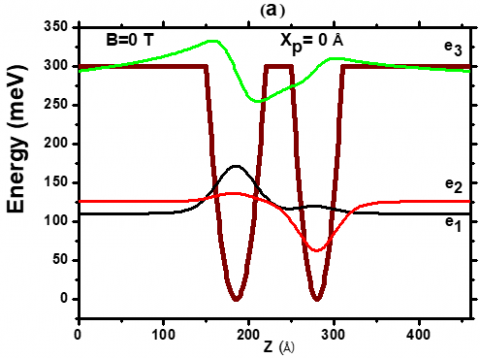
Figure 1. The variation of the confinement potential profile the conduction band, ground, first and second excited states and their wave functions for different values of the thickness step xp and magnetic field
Figure 1 depicts schematically the confinement potential profile and the energy levels with their wave functions along the z direction for different values of applied external magnetic field and thickness step xp. For example, for the step xp=6Å the thickness of layers of the structure becomes as follows: Lw1=73Å, Lw2=63Å, Lb2=24Å, Lb1=Lb3=150Å. From Figure 1 (a), (b), (c), (d), one can clearly see that the magnetic field affects strongly on the confined potential, which consequently leads to a direct effect on the energies and their wave functions. This can be explained by the effect of the potential V(z) on the solutions of Schrödinger equation. The sharp parts in the confinement potential profile at interfaces between layers (see Figure 1 (c), (d),) where these sharp parts are resulting from the change of the effective mass in each layer and depends the term $\frac{e^2 B^2}{2 m^*(z)} Z^2$ in Eq. (2). It is also worth mentioning that an increase in magnetic field B leads to the augmentation of the confinement potential profile along the z direction and the top of the conduction band takes parabolic form. In addition, we see that in the case of the absence of magnetic field the wave function of the ground state has a greater localization in the first well (left well) than the second well (right well), while the wave function of the first excited state has a greater localization in the second well (right well) than the first well (left well). But in the case of the presence of the magnetic field we note that the wave function of the ground state most their distribution is localized in first well, unlike the case of the wave function of the first excited state most their distribution is localized d in the second well. This means that the greater localization appeared in the left well is due to the probability of the existence of an electron in the level 1, unlike in level 2 (first excited state) where the greater probability is in the right well.
Figure 2. The variation of energy separation between grand state and the first excided state as a function of (a) thickness step xp; (b) magnetic field
Figure 2 displays the variation of the energy transition E2-E1 as a function of thickness step xp and magnetic field. In Figure 2 (a), we present the energy transition as a function of the $x_p$ parameter for four different values of the magnetic field 0, 4, 8 and 12T respectively, this Figure 2, clearly indicates that the effect of the thickness layers (xp) on the energy transition is not significant, especially for B=0 and B=4T, and we can be see that for B>4T with the augmentation of xp parameter leads to reduce the values of E2- E1. Whereas Figure 2 (b), presents the transition energy as a function of the magnetic field for four values of the thickness step parameter which equal to 0, 6, 12 and 18Å respectively. This Figure 2 (b), shows clearly that the energy separation dependence with magnetic field, this latter (magnetic field) when increase, we note that the difference energy becomes larger. In addition, the curves are staying close each other for different values of the thickness step xp, so, the energy transition E2- E1 is almost insensitive to variations of thickness of layers. Therefore, we can be concluding that the potential is more affected by the magnetic field than the thickness of the structure, and its variation modifies strongly the energy level values of the quantum system. The behavior of E2 - E1 is explained by the following reason, the magnetic field has an important effect and contribution on the potential profile as seen in Figure 1.
Figure 3 represents the evolution of the absolute value of dipole matrix element as a function of the thickness step parameter and magnetic field. In Figure 3 (a), we depict the variation of the absolute value of dipole matrix element as a function of the thickness step for different values of magnetic field, from this Figure 3 (a), we see that the values of dipole matrix element increase on quasi linear manner with thickness step parameter, while in Figure 3(b), we draw the variation of the absolute value of dipole matrix element as a function of the magnetic field for different values of the thickness step, which indicate that it is decreasing rapidly with increasing the magnetic field, but when reaches a small certain value is decreasing very slowly. And thus, from the Figure 3, we see clearly that both the magnetic field and thickness of layers of the structure take a dominant role in the dipole matrix element. This behavior is related to the overlap between the eigenfunctions corresponding to ground and the first excited electronic states.
Figure 3. The variation of absolute value of dipole matrix element for (1-2) ISBT as a function a) thickness step; b) magnetic field
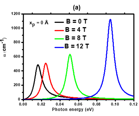
Figure 4 displays the variation of optical absorption coefficient, for four different values of external applied magnetic field (0, 4, 8, and 12T) corresponding to four values of the thickness step (0, 6, 12, and 18Å), as a function of the incident photon energy. It is remarkable that the resonant peak position of OAC moves to higher energies by increasing the applied magnetic field, and its magnitude increases nonlinearly. This behavior of OAC is strongly related to difference energy. We see also when we increment the values of xp in a way mentioned in theoretical section, that the magnitude of OAC increases, for example, when B=0T with varying the parameter xp from 0 to 18Å that leads to increases the OAC from 485.4 to 2215.25 cm-1 respectively (see Figure 4 (a), (c)), but the corresponding resonant peak position is slightly shifted compared with the effect of magnetic field which we can be considered it constant(remains almost at the same position for different values of thickness step parameter). According to Eq. (6) we can be note easily that the optical absorption coefficient is related strongly to a square of the dipole matrix element and also with a square of energy separation in Lorentzian term in the same Eq. (7).
Figure 4. The variation of the optical absorption coefficient as a function of photon energy for different values of magnetic field and thickness step
Figure 5. The variation of refractive index changes as a function of the incident photon energy as a function of photon energy for different values of the magnetic field and thickness step
In Figure 5, we show schematically the variation of RICs as a function of the incident photon energy in the range from 0 to 120meV corresponding the transition (1-2) occurs between the ground and first excited states for cases with and without the magnetic field with xp values of 0, 6, 12, and 18Å, respectively. According to Figure 5 (a), (b), (c), (d), we can also observe obviously that the increasing of the magnetic field leads to significant variation of the peak position the RICs and as shifting in toward higher energies (blue shift) with decrease the magnitude of the resonant peak. Whereas, we can notice that the magnitude of the resonant peak increases when the xp parameter increases. In addition, the parameter xp has a too small effect on the position of the resonant peak compared to the resulting effect of the magnetic field. This behavior can be explained by the more sensibility of E2-E1 to B than xp parameter as can be seen in Figure 2.
In this research, we have treated numerically the effects of both the thickness of layers and magnetic field from 0 to 12T on the linear OAC and RICs for intersubband electronic transition (1-2) of the AlGaAs/GaAs double parabolic quantum wells. The first important result shows that the peak positions, in both cases of OAC and RICs are more sensitive to the effect of the applied magnetic field than to the effect of thickness step xp. It has also been shown that for both OAC and RICs, the resonant peak positions are insensitive to the thickness of layers and considerably shifted toward higher energies when increasing applied magnetic field. On the other hand, for both the OAC and RICs, the resonant peak magnitudes are strongly affected by the thickness of layers when varying the step xp from 0 to 18Å. These numerical results indicate that the thickness of layers and magnetic field play a major role in tuning of the OAC and RICs and their controlling.
The authors would like to thank the (DGRSDT) of the Algerian Ministry of Higher Education and Scientific Research for the support and encouragement the scientific research.
[1] Kazarinov, R.F. (1971). Possibility of application of electromagnetic waves in a semiconductor with a superlattice. Soviet Physics Semiconductors Ussr, 5(4): 707-709.
[2] Capasso, F., Mohammed, K., Cho, A.Y. (1986). Electronic transport and depletion of quantum wells by tunneling through deep levels in semiconductor superlattices. Physical Review Letters, 57(18): 2303. http://dx.doi.org/10.1103/PhysRevLett.57.2303
[3] Miller, D.A. (1990). Quantum well optoelectronic switching devices. International Journal of High Speed Electronics and Systems, 1(1): 19-46. http://dx.doi.org/10.1142/S0129156490000034
[4] Chang, L.L., Esaki, L., Howard, W.E., Ludeke, R., Schul, G. (1973). Structures grown by molecular beam epitaxy. Journal of Vacuum Science and Technology, 10(5): 655-662. http://dx.doi.org/10.1116/1.1318408
[5] Hasenberg, T.C., Day, P.S., Shaw, E.M., Magarrell, D.J., Olesberg, J.T., Yu, C., Flátte, M.E. (2000). Molecular beam epitaxy growth and characterization of broken-gap (type II) superlattices and quantum wells for midwave-infrared laser diodes. Journal of Vacuum Science & Technology B: Microelectronics and Nanometer Structures Processing, Measurement, and Phenomena, 18(3): 1623-1627. http://dx.doi.org/10.1116/1.591440
[6] Qi, X.H., Kong, X.J., Liu, J.J. (1998). Effect of a spatially dependent effective mass on the hydrogenic impurity binding energy in a finite parabolic quantum well. Physical Review B, 58(16): 10578. http://dx.doi.org/10.1103/PhysRevB.58.10578
[7] Waag, A., Fischer, F., Lugauer, H.J., Litz, T., Laubender, J., Lunz, U., Landwehr, G. (1996). Molecular‐beam epitaxy of beryllium‐chalcogenide‐based thin films and quantum‐well structures. Journal of Applied Physics, 80(2): 792-796. http://dx.doi.org/10.1063/1.362888
[8] Levine, B.F., Choi, K.K., Bethea, C.G., Walker, J., Malik, R.J. (1987). New 10 μm infrared detector using intersubband absorption in resonant tunneling GaAlAs superlattices. Applied Physics Letters, 50(16): 1092-1094. http://dx.doi.org/10.1063/1.97928
[9] Kazarinov, R.F., Suris, R.A. (1972). Electric and electromagnetic properties of semiconductors with a superlattice. Soviet Physics Semiconductors Ussr, 6(1): 120-131.
[10] Ahn, D., Chuang, S.L. (1987). Calculation of linear and nonlinear intersubband optical absorptions in a quantum well model with an applied electric field. IEEE Journal of Quantum Electronics, 23(12): 2196-2204. http://dx.doi.org/10.1109/JQE.1987.1073280
[11] Harwit, A., Harris Jr, J.S. (1987). Observation of Stark shifts in quantum well intersubband transitions. Applied Physics Letters, 50(11): 685-687. http://dx.doi.org/10.1063/1.98066
[12] Ungan, F., Mora-Ramos, M. E., Kasapoglu, E., Sari, H., Sökmen, I. (2019). Nonlinear optical properties of triple δ-doped quantum wells: the impact of the applied external fields. Optik, 180: 387-393. http://dx.doi.org/10.1016/j.ijleo.2018.11.120
[13] Sari, H., Ungan, F., Sakiroglu, S., Yesilgul, U., Sökmen, I. (2018). The effects of intense laser field on optical responses of n-type delta doped GaAs quantum well under applied electric and magnetic fields. Optik, 162: 76-80. http://dx.doi.org/10.1016/j.ijleo.2018.02.092
[14] El Kadadra, A., Fellaoui, K., Abouelaoualim, D., Oueriagli, A. (2016). Optical absorption coefficients in GaN/Al (Ga) N double inverse parabolic quantum wells under static external electric field. Modern Physics Letters B, 30(25): 1650165. http://dx.doi.org/10.1142/S0217984916501657
[15] Guo, A., Du, J. (2013). Linear and nonlinear optical absorption coefficients and refractive index changes in asymmetrical Gaussian potential quantum wells with applied electric field. Superlattices and Microstructures, 64: 158-166. http://dx.doi.org/10.1016/j.spmi.2013.08.030
[16] Yesilgul, U. (2012). Linear and nonlinear intersubband optical absorption coefficients and refractive index changes in symmetric double semi-V-shaped quantum wells. Journal of Luminescence, 132(3): 765-773. http://dx.doi.org/10.1016/j.jlumin.2011.10.016
[17] Kasapoglu, E.S.İ.N., Duque, C.A., Mora-Ramos, M.E., Restrepo, R.L., Ungan, F.A.T.İ.H., Yesilgul, U., Sökmen, I. (2015). Combined effects of intense laser field, electric and magnetic fields on the nonlinear optical properties of the step-like quantum well. Materials Chemistry and Physics, 154: 170-175. http://dx.doi.org/10.1016/j.matchemphys.2015.01.010
[18] Zhu, J., Ban, S.L., Ha, S.H. (2013). A simulation of intersubband absorption in ZnO/MgxZn1-xO quantum wells with an external electric field. Superlattices and Microstructures, 56: 92-98. http://dx.doi.org/10.1016/j.spmi.2012.11.011
[19] Ozturk, E.M.İ.N.E., Sokmen, I. (2013). Electric field effect on the nonlinear optical absorption in double semi-graded quantum wells. Optics Communications, 305: 228-235. http://dx.doi.org/10.1016/j.optcom.2013.05.021
[20] Alaydin, B.O., Altun, D., Ozturk, E. (2022). Linear and nonlinear optical properties of semi-elliptical InAs quantum dots: Effects of wetting layer thickness and electric field. Thin Solid Films, 755: 139322. http://dx.doi.org/10.1016/j.tsf.2022.139322
[21] Sayrac, M., Kaynar, E., Ungan, F. (2023). The effect of structure parameters and static electric field on the nonlinear optical properties of triple InGaAs/GaAs quantum well. Journal of Molecular Structure, 1273: 134252. http://dx.doi.org/10.1016/j.molstruc.2022.134252
[22] Ozturk, E.M.İ.N.E., Sokmen, I. (2010). Intersubband optical absorption coefficients and refractive index changes in triple quantum well with different well shapes. The European Physical Journal-Applied Physics, 51(1): 10303. http://dx.doi.org/10.1051/epjap/2010068
[23] Aytekin, O., Turgut, S., Tomak, M. (2012). Nonlinear optical properties of a Pöschl-Teller quantum well under electric and magnetic fields. Physica E: Low-dimensional Systems and Nanostructures, 44(7-8): 1612-1616. http://dx.doi.org/10.1016/j.physe.2012.04.005
[24] Dakhlaoui, H., Nefzi, M. (2019). Tuning the linear and nonlinear optical properties in double and triple δ- doped GaAs semiconductor: Impact of electric and magnetic fields. Superlattices and Microstructures, 136: 106292. http://dx.doi.org/10.1016/j.spmi.2019.106292
[25] Harrison, P. (2005). Quantum wells, wires and dots: Theoretical and computational physics of semiconductor nanostructures. John Wiley & Sons. http://dx.doi.org/10.1002/0470010827
[26] Ahn, D., Chuang, S.L. (1987). Nonlinear intersubband optical absorption in a semiconductor quantum well. Journal of Applied Physics, 62(7): 3052-3055. http://dx.doi.org/10.1063/1.339369