Asma Benchiheb*![]() | Samira Dib
| Samira Dib![]() | Nedjoua Benchiheb
| Nedjoua Benchiheb![]() | Yasmina Saidi
| Yasmina Saidi![]() | Hamza Lidjici
| Hamza Lidjici![]()
© 2023 IIETA. This article is published by IIETA and is licensed under the CC BY 4.0 license (http://creativecommons.org/licenses/by/4.0/).
OPEN ACCESS
This study delves into the pervasive role of Auger recombination as an intrinsic carrier recombination process in silicon solar cells, critically influencing their performance parameters such as short circuit current density, open circuit voltage, efficiency, and fill factor. The objective is to attenuate this effect by optimizing the doping level and the emitter's scattering depth in an N+PP+-type silicon solar cell. The COMSOL software was utilized for simulations, assessing the impacts of varied doping levels and emitter thicknesses. It was observed that Auger recombination effects are insignificant at low doping levels but become predominant at higher doping levels, particularly with increased emitter thicknesses. Notably, a substantial enhancement in performance parameters was achieved by reducing the emitter thickness to approximately 0.4-0.6 µm and heavily doping the emitter surface to the order of ~1020 cm-3. The optimal performance was realized at a thickness of 0.4 µm, and it was found that the implications of the Auger recombination effect surpassed those of the Shockley-Read-Hall recombination effects. These findings bear significant implications for optimizing solar cell design, enabling the production of solar panels with superior electrical efficiency.
silicon solar cells, auger recombination, doping optimization, emitter thickness, simulation, COMSOL software
The quest for novel energy sources, ignited by the 19th-century industrial revolution, has precipitated the emergence of a competitive sector fraught with challenges for many nations. Presently, fossil fuels account for 80% of the world's energy supply. Regrettably, these sources not only pose environmental concerns, but their progressive depletion is also increasingly evident. This has been substantiated by the Energy Watch Group and the International Energy Agency, indicating that over half of the world's crude oil reserves have been exhausted [1, 2]. Consequently, numerous nations have adopted the exploitation of renewable resources, particularly photovoltaics, as a mitigation strategy.
Silicon-based solar panels, owing to the abundance of silicon in the form of quartz, continue to command the photovoltaic industry. Nonetheless, their efficiency is constrained to 20-30%, presenting a significant limitation [3].
Various solutions have been proposed to circumvent this issue, including perovskite-silicon tandems or multi-junction technologies [4-6], double-sided cell architectures [7-11], and emitter region optimization approaches [12-14]. Upon scrutiny, multi-junction structures' most glaring disadvantage is their relatively high-cost compared to unijunction cell technologies. However, cell models premised on emitter region optimization have facilitated the manufacture of solar panels with continually increasing efficiencies, particularly for silicon-based cells. Indeed, Redfield and Dziewior's work [15, 16] established that solar cell performance degradation is principally attributed to Auger recombination, which ensues when the transmitter's doping level exceeds a certain threshold. Subsequently, research by Stem and Cid [17], Subramanian et al. [13], and Thirunavukkarasu et al. [12] demonstrated that efficiency and open-circuit voltage could be maximized and the solar cell's blue response improved by optimizing the emitter doping level [13, 18].
In this paper, we propose a novel optimization approach for the silicon solar cell structure, considering the doping level and diffusion depth of the emitter to minimize the effect of Auger recombination. This effect, typically found in semiconductors with high doping levels and an indirect gap, induces a reduction in carrier minority lifetime and their diffusion length in the emitter region, resulting in a degradation of the output parameters and electrical characteristics [16, 18].
The optimization of the emitter layer is based on simulations that help understand and predict the performance of the electronic device while varying the semiconductor material's electrical and physical properties. Given that the emitter formation phase in the solar cell manufacturing process is complex and costly, it is always advisable to perform simulations ahead of any experimental verification of the performance of the optimized emitter configurations [19].
COMSOL Multiphysics software [20], renowned for modeling and solving diverse scientific and engineering problems, was employed for the study. It allows for the processing of various physical phenomena simultaneously, thanks to pre-integrated models and physical parameters, or those implemented to solve a specific problem [20-23]. Despite requiring no extensive knowledge of mathematics and physics, COMSOL provides interfaces to describe the mathematical application modes of the PDE, facilitating different analyses, including stationary and temporal analyses.
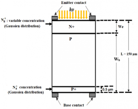
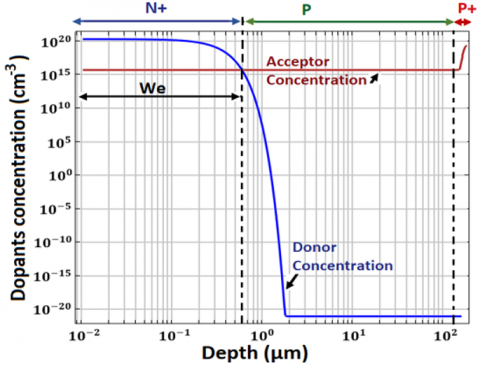
The overall structure and the doping profile of the investigated solar cell are illustrated in Figure 1 and Table 1, respectively. The parameters are carefully selected using the literature [12, 13, 18, 19, 24, 25].
The device is composed of three layers:
(a) General structure
(b) Doping profile
Figure 1. General structure and doping profile of the studied silicon solar cells
According to the literature, the doping concentration of monocrystalline silicon wafers varies from 1×1012 cm-3 to 1× 1020cm-3 [19]. Even though a high level of the P-type substrate’s doping improves the open circuit voltage (Voc) [26], it reduces the lifetime and carrier mobility. Hence the efficiency decreases. Furthermore, a low P-type doping concentration has a negative consequence [19]. For this purpose, moderate doping of the P-type silicon wafers is essential. Thus, the doping concentration of the silicon wafer was adjusted to 5×1015 cm-3 [24].
The introduction of a highly doped layer (P+) on the back side of the wafer allows the production of a back surface field (BSF). This BSF is used as a means to improve the performance of the solar cell by reducing the surface recombination velocity (SRV) [27-29].
The key to improving the efficiency of solar cells lies in increasing the lifetime of the minority carriers [30]. Indeed, in these structures, the carriers are continuously generated, and for this purpose, the lifetime value determines the stable population of electrons and holes. This population should be desirably as large as possible to maximize the voltage produced by the structure [31]. As in references [12, 13, 18], a minority-carrier lifetime of 100 µs was assumed, but much longer carrier lifetimes have been achieved, thanks to the combined effects of gettering, hydrogenation, and improved ingot growth technologies [18].
Table 1. Values of technological and physical parameters
|
Solar Cell Parameter |
N+- P – P+ |
|
|
Emitter doping profile |
Gaussian |
|
|
Surface concentration |
Nd+ (variable) |
|
|
Thickness |
We (variable) |
|
|
Substrate concentration Thickness |
Na=5 ×1015 cm-3 (Uniform distribution) |
[24] |
|
|
L=150 µm |
[18, 24] |
|
P+ diffusion: doping profile |
Gaussian |
|
|
Back surface concentration |
Na+=3.6 ×1019 cm-3 |
[12, 25] |
|
Thickness |
WNa+=0.5 µm |
[18] |
|
T |
25℃ |
|
|
Recombination lifetime in the Bulk |
100 µs |
[12, 13, 18] |
The DDM model (Drift-Diffusion Model) is used by COMSOL to simulate the electronic structure. This software's simulation of solar cells is based on the numerical resolution using the finite element method [20] of the continuity and transport equations as well as the Poisson equation [14, 32]:
$\operatorname{div}(\epsilon \cdot \overrightarrow{\operatorname{grad}} V)=-\rho$ (1)
$g_n-r_n=-\frac{1}{q} \vec{\nabla} \overrightarrow{J_n}$ (2)
$g_p-r_p=\frac{1}{q} \vec{\nabla} \overrightarrow{J_p}$ (3)
$\overrightarrow{J_n}=q n \mu_n \vec{E}+q D_n \vec{\nabla} n$ (4)
$\overrightarrow{J_p}=q p \mu_p \vec{E}-q D_p \vec{\nabla} p$ (5)
where,
$\rho=q \cdot\left(p-n+d o p+n_t\right)$ (6)
where, $\mu_n$ and $\mu_p$ are calculated according to the Arora model [33].
Regarding the recombination term, two types of recombination are considered: Auger and Shockley–Read–Hall (SRH) recombination.
Auger recombination is traditionally described as a nonradiative band-to-band event involving three particles. In this process, an electron and hole from the conduction and valence bands recombine, and the surplus energy is transmitted to a third free electron or hole, which is moved to a higher energy level.
Commonly, the following equation is used to simulate Auger recombination [15, 34]:
$r_{\text {Auger }}=C_n\left(p n^2-n n_{i e}^2\right)+C_p\left(n p^2-p n_{i e}^2\right)$ (7)
In an SRH-type recombination process, electron–hole pairs recombine through impurities or deep-level traps, and the liberated energy is dissipated by lattice vibrations or phonons. The bulk SRH recombination rate is given [32].
$r_{S R H}=\frac{n \cdot p-n_i^2}{\tau_p \cdot\left(n+n_1\right)+\tau_n \cdot\left(p+p_1\right)}$ (8)
where,
$\begin{gathered}n_1=n_i \cdot \exp \left[\left(E_T-E_i\right) / k_B T\right] \\ p_1=n_i \cdot \exp \left[-\left(E_T-E_i\right) / k_B T\right]\end{gathered}$ (9)
Under illumination, the following equation [32] is used to compute the photo-generation rate for each wavelength:
$G(\lambda, x)=\alpha(\lambda) \cdot F(\lambda) \cdot(1-R(\lambda)) \cdot e^{-\alpha(\lambda) \cdot x}$ (10)
$\alpha(\lambda)$ is the absorption coefficient at wavelength $\lambda, F(\lambda)$ is the number of incident photons/cm2/s per unit bandwidth, and R(λ) is the proportion of photons reflected off the surface.
The overall photo-generation rate $G(x)$ is the integral of Eq. (10) across all sun spectrum wavelengths.
The results presented in this section illustrate the impact of modifications in doping and emitter layer thickness on the various solar cell parameters. This analysis examines two instances:
Table 2. The thickness of the various layers taken into account
|
j |
We (µm) |
|
1 |
2 |
|
2 |
1.5 |
|
3 |
1 |
|
4 |
0.6 |
|
5 |
0.4 |
In this study, we considered different emitter layer thicknesses (We) between 0.4 µm and 2 µm. Each layer thickness is identified by an index j, as indicated in Table 2.
4.1 Effects on short-circuit current density
4.1.1 In the ideal case
Figure 2 illustrates the short-circuit current density variation in the ideal case versus the emitter surface doping concentration (Nd+) for different emitter thicknesses We.
These curves are a result of the photo-generation effects that occur when a solar cell is exposed to light. Under illumination, electron-hole pairs are produced precisely where photons are absorbed. If this phenomenon occurs within or close to the depletion zone, where an electric field prevails, this field will contribute to separating the positive charges from the negative charges so that the electrons are repelled towards the n-type layer and the holes to the p-type layer.
The electrons still seeking to recombine with the holes are then forced to pass through the external circuit to join them, thus creating a photo-current.
Reducing the emitter thickness, We, will allow:
Figure 2. Variation in the short-circuit current density at the ideal case versus the surface emitter doping, $N_d^{+}$, at different emitter thicknesses We: 0.4 µm, 0.6 µm, 1 µm, 1.5 µm, 2 µm
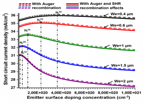
4.1.2 With Auger and SHR recombination
Figure 3 illustrates the short-circuit current density variation in which Auger recombination effects are taken into account.
In this case, the curves reveal a minor rise in the $J_{sc}$ current density as a function of surface emitter doping $N_d^{+}$, followed by a reduction from a specific threshold emitter surface doping level $N_J$.
For each $j^{t h}$ emitter thickness layer, the threshold $N_J^{(j)}$ is chosen at the point where the short-circuit current density is maximum. The (maximum) current density at this point is denoted $J_{s c}\left(d o p=N_J^{(j)}\right)$.
Thus, at the point of surface emitter doping $N_d^{+}$ equal to 1021cm-3, the corresponding short-circuit density is denoted $J_{s c}\left(d o p=10^{21} \mathrm{~cm}^{-3}\right)$.
For each $j^{t h}$ emitter thickness layer, we define the decay rate in current density $\Delta J_{sc}$ as:
$\Delta J_{s c}=J_{s c}\left(d o p=N_J^{(j)}\right)-J_{s c}\left(d o p=10^{21} \mathrm{~cm}^{-3}\right)$ (11)
Taking into account only Auger-type recombination effects, Figure 3 demonstrates a slight increase in $J_{s c}$ values for doping levels below the threshold $N_J^{(j)}$ and a drop when the emitter surface doping is above this threshold.
Moreover, as shown in Table 3, we note that:
Figure 3. Variation in the short-circuit current density with Auger and SRH recombination effects versus the surface emitter doping, $N_d^{+}$, at different emitter thicknesses We: 0.4 µm, 0.6 µm, 1 µm, 1.5 µm, 2 µm
Table 3. Short-circuit current density parameters in the presence of Auger recombination
|
j |
NJ(j) |
Jsc(dop=NJ(j)) |
Jsc(dop=1021cm-3) |
ΔJsc |
|
|
(cm-3) |
mA/cm2 |
mA/cm2 |
mA/cm2 |
|
1 |
2.00×10¹⁹ |
31.152289 |
27.294474 |
3.857815 |
|
2 |
3.80×10¹⁹ |
32.271672 |
29.285420 |
2.986252 |
|
3 |
8.20×10¹⁹ |
33.691673 |
31.762171 |
1.929502 |
|
4 |
2.13×10²⁰ |
35.198529 |
34.257704 |
0.940826 |
|
5 |
3.34×10²⁰ |
36.125018 |
35.707377 |
0.417640 |
If, in addition to the effects of Auger recombination, the impacts of SRH recombination are taken into account, it is noted that for each thickness j, another modest additional drop in the short-circuit current density can be observed. Moreover, Table 4 shows that the threshold $N_J^{(j)}$ remains relatively unchanged.
These results demonstrate that in a solar cell, Auger recombination reduces the number of minority carriers participating in the photocurrent. However, this phenomenon only occurs from a certain determined level of doping. This explains the shape of the curve of the short-circuit current density which decreases from a certain threshold doping level $N_J^{(j)}$. It is also noted that the presence of SHR recombination also reduces the number of minority carriers, which results in an additional drop in the photocurrent and, therefore, in the short-circuit current density.
By reducing the thickness of the emitter layer to the order of 0.4 - 0.6 µm, a significant improvement in the short-circuit current is observed. This result agrees with the results of the work of Ghosh et al. [35]. Furthermore, Stem and Cid [17] also confirmed that the best $J_{sc}$ is obtained for an emitter thickness of around 0.4 µm.
Table 4. Short-circuit current density parameters in the presence of Auger and SHR recombination
|
j |
NJ(j) |
Jsc (dop=NJ(j)) |
Jsc(dop=1021cm-3) |
ΔJsc |
|
|
(cm-3) |
mA/cm2 |
mA/cm2 |
mA/cm2 |
|
1 |
2.00×10¹⁹ |
31.018552 |
27.159568 |
3.858984 |
|
2 |
3.50×10¹⁹ |
32.135581 |
29.148162 |
2.987419 |
|
3 |
8.40×10¹⁹ |
33.55034 |
31.617932 |
1.932408 |
|
4 |
1.92×10²⁰ |
35.050800 |
34.110544 |
0.940256 |
|
5 |
3.37×10²⁰ |
35.978421 |
35.560789 |
0.417632 |
4.2 Effects on open-circuit voltage
4.2.1 In the ideal case
Regarding the variations of the open-circuit voltage, in the ideal case, Figure 4 shows that the increase in ${N}_d{ }^{+}$ doping concentration induces an increase in the Voc values. For doping levels, less than the threshold value $N_{v o c}$ of about $2 \times 10^{20} \mathrm{~cm}^{-3}$, Voc increases significantly before reaching a steady state. Indeed, beyond $N_{v o c}$, Voc does not increase much further. In addition, increasing the emitter layer thickness improves the Voc values only for surface doping concentration, ${N}_d{ }^{+}$, below $N_{v o c}$. Above this threshold value, an opposite behaviour is observed.
Figure 4. Variation in the open circuit voltage density at the ideal case versus the surface emitter doping (for different emitter thicknesses We: 0.4 µm, 0.6 µm, 1 µm, 1.5 µm, 2 µm)
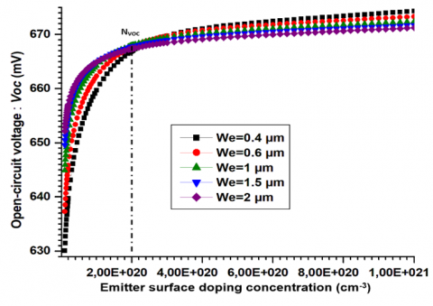
4.2.2 With Auger and SHR recombination
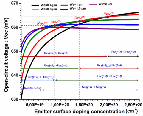
Figure 5 shows the open-circuit voltage variation in which Auger recombination effects are taken into account. In this case, we observe that:
As specified in Figure 6 and Table 5, if we define Nvoc(j1) at the intersection point of two Voc curves corresponding to two consecutive thicknesses j1 and j2 such that: j2=j1+1 and Voc(j1)=Voc(j2).
We notice that:
Figure 5. Variation in the open circuit voltage density with Auger and SRH recombination effects versus the surface emitter doping at different emitter thicknesses We: 0.4 µm, 0.6 µm, 1 µm, 1.5 µm, 2 µm
Table 5. Voc parameters in the presence of Auger recombination
|
Nvoc (j)(cm-3) |
Voc (mV) |
|
Nvoc(1)=5.21083172×10¹⁹ |
659.791183 |
|
Nvoc(2)=7.96131528×10¹⁹ |
660.881674 |
|
Nvoc(3)=1.27208253×10²⁰ |
662.552201 |
|
Nvoc(4)=1.85278315×10²⁰ |
664.431555 |
Figure 6. Zoom on the variation in the open circuit voltage density with Auger recombination effects versus the surface emitter doping (at different emitter thicknesses We: 0.4 µm, 0.6 µm, 1 µm, 1.5 µm, 2 µm) with Auger recombination effect
Figure 7. Zoom on the variation in the open circuit voltage density with Auger and SRH recombination effects versus the surface emitter doping (at different emitter thicknesses We: 0.4 µm, 0.6 µm, 1 µm, 1.5 µm, 2 µm) with Auger recombination effect
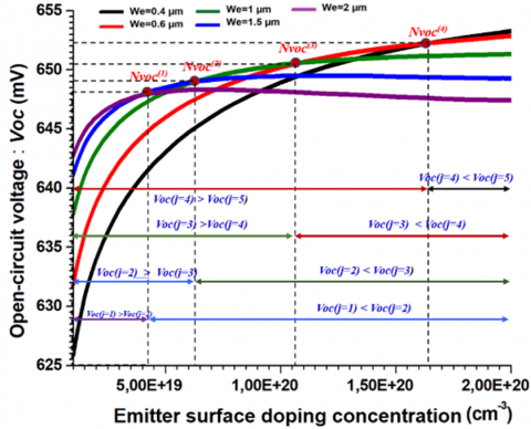
If SRH recombination are considered in addition to the Auger-type recombination effects, a reduction in Voc of the order of 13 mV is obtained without a little modification in Nvoc (j) for a given thickness (We) as confirmed by Figure 7 and the Table 6. Thus, in this case, the optimal value of We remains identical to that chosen in the case of the presence of Auger recombination only.
Table 6. Voc parameters in the presence of Auger and SHR recombination
|
Nvoc(j) (cm-3) |
Voc (mV) |
|
Nvoc(1)=3.8757790×10¹⁹ |
647.832077 |
|
Nvoc(2)=6.2830432×10¹⁹ |
649.066125 |
|
Nvoc(3)=1.08091554×10²⁰ |
650.585847 |
|
Nvoc(4)=1.66827853×10²⁰ |
652.320186 |
4.3 Effects on fill factor
4.3.1 In the ideal case
Concerning the variations of the fill factor in the ideal case, Figure 8 shows the following:
4.3.2 With Auger and SHR recombination
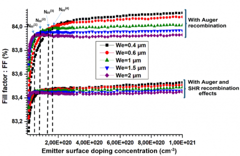
By considering Auger recombination, Figure 9 shows that this effect causes an overall drop in the FF compared to the ideal case and that the threshold doping value NFF is no longer unique or constant but instead depends on the considered emitter layer thickness.
As specified in Table 7, if we define NFF(j1) at the intersection point of two Voc curves corresponding to two consecutive thicknesses j1 and j2 such that: j2=j1+1 and Voc(j1)=Voc(j2).
We notice that:
If SRH recombination effects are included in addition to Auger-type recombination effects, the FF reduces by around 0.5%, without a little modification in NFF(j) for a given thickness (We) as confirmed by Table 8. Thus, in this case, the optimal value of We remains identical to that chosen in the case of the presence of Auger recombination only.
Figure 8. Variation in the fill factor at the ideal case versus the surface emitter doping at different emitter thicknesses We: 0.4 µm, 0.6 µm, 1 µm, 1.5 µm, 2 µm
Figure 9. Variation in the fill factor with Auger and SRH recombination effects versus the surface emitter doping at different emitter thicknesses We: 0.4 µm, 0.6 µm, 1 µm, 1.5 µm, 2 µm
Table 7. Fill factor parameters in the presence of Auger recombination
|
NFF(j) (cm-3) |
FF (%) |
|
NFF(1)=5.33247367×10¹⁹ |
83.9307425 |
|
NFF(2)=9.39952719×10¹⁹ |
83.9570766 |
|
NFF(3)=1.29194068×10²⁰ |
83.9784803 |
|
NFF(4)=1.96039115×10²⁰ |
84.0109774 |
Table 8. Fill factor parameters in the presence of Auger recombination and SHR recombination
|
NFF(j) (cm-3) |
FF (%) |
|
NFF(1)=3.0199226×10¹⁹ |
83.4399594 |
|
NFF(2)=4.84487427×10¹⁹ |
83.4547506 |
|
NFF(3)=1.03411992×10²⁰ |
83.4652523 |
|
NFF(4)=1.49357834×10²⁰ |
83.4747187 |
4.4 Effects on conversion efficiency
4.4.1 In the ideal case
Figure 10 illustrates the variations of the conversion efficiency versus the emitter surface doping concentration (${N}_d{ }^{+}$) in the ideal case. It is observed that the efficiency $\eta$ is proportional to the emitter surface doping ${N}_d{ }^{+}$ but inversely proportional to its layer thickness We.
To interpret this result, it suffices to consider the theoretical equation which makes it possible to calculate this term. This equation is given [26]:
$\eta=\frac{F F \cdot V o c \cdot J_{S c}}{P_i}$ (11)
Since the three terms $J_{s c}, Voc$, and FF depend on doping and reducing the emitter thickness layer makes it possible to improve them, this explains, why this conversion factor increases with the doping and can also be enhanced by lowering We.
Figure 10. Variation in the conversion efficiency at the ideal case versus the surface emitter doping (for different emitter thicknesses We: 0.4 µm, 0.6 µm, 1 µm, 1.5 µm, 2 µm)
4.4.2 With Auger and SHR recombination
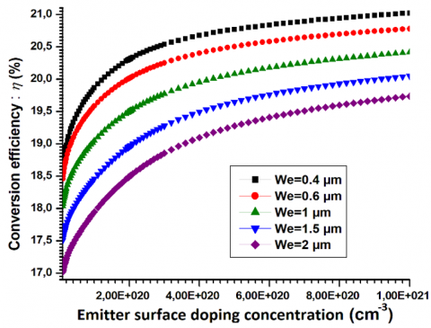
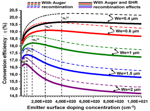
Figure 11 shows the variations of the conversion efficiency versus the emitter surface doping concentration (${N}_d{ }^{+}$) for different emitter thicknesses We and with the presence of recombination effects.
For each $j^{ {th }}$ emitter thickness layer, the threshold Nƞ (j)is chosen at the point where the conversion efficiency is maximum. The (maximum) the conversion efficiency at this point is denoted ƞ (dop=Nƞ (j)).
Thus, at the point of surface emitter doping ${N}_d{ }^{+}$ equal to 1021cm-3, the corresponding conversion efficiency is denoted $\eta$ (dop=1021cm-3)
For each $j^{ {th }}$ emitter thickness layer, we define the decay rate in conversion efficiency $\Delta \eta$ as:
$\Delta \eta=\eta\left(d o p=N_{\mathrm{\eta}}^{(j)}\right)-\eta\left(d o p=10^{21} c m^{-3}\right)$ (12)
Figure 11. Variation in the conversion efficiency with Auger and SRH recombination effects versus the surface emitter doping (for different emitter thicknesses We: 0.4 µm, 0.6 µm, 1 µm, 1.5 µm, 2 µm)
Taking into account only Auger-type recombination effects, Figure 11 demonstrates a slight increase in ƞ values for doping levels below the threshold Nƞ(j)and a drop when the emitter surface doping is above this threshold.
As shown in Table 9, the following observations are also made:
Table 9. Conversion efficiency parameters in the presence of Auger
|
j |
Nƞ(j) |
ƞ (dop=Nƞ (j)) |
ƞ (dop=1021cm-3) |
Δƞ |
|
|
(cm-3) |
% |
% |
% |
|
1 |
3.6×10¹⁹ |
17.193501 |
15.111630 |
2.081871 |
|
2 |
5.5×10¹⁹ |
17.858131 |
16.277215 |
1.580916 |
|
3 |
1.1×10²⁰ |
18.718527 |
17.744468 |
0.974059 |
|
4 |
2.5×10²⁰ |
19.668842 |
19.252838 |
0.416003 |
|
5 |
4.2×10²⁰ |
20.285696 |
20.155714 |
0.129982 |
Table 10. Conversion efficiency parameters in the presence of Auger and SHR recombination
|
j |
Nƞ(j) |
ƞ (dop=Nƞ (j)) |
ƞ (dop=1021cm-3) |
Δƞ |
|
|
(cm-3) |
% |
% |
% |
|
1 |
3.0×10¹⁹ |
16.740882 |
14.674279 |
2.066604 |
|
2 |
5.0×10¹⁹ |
17.382161 |
15.805496 |
1.576665 |
|
3 |
1.0×10²⁰ |
18.207211 |
17.226840 |
0.980371 |
|
4 |
2.4×10²⁰ |
19.106923 |
18.681007 |
0.425917 |
|
5 |
4.0×10²⁰ |
19.685409 |
19.554035 |
0.131374 |
If the effects of SRH recombination are added to the effects of Auger recombination, an additional drop in efficiency is noticed. However, its influence remains very moderate as compared to that of Auger recombination effects when evaluated alone. Nevertheless, as reported in the Table 10, the variation of the threshold Nƞ(j)associated with the layer thickness j remains very limited.
These results demonstrate that the presence of Auger-type recombination contributes to reducing the conversion efficiency. However, this phenomenon only occurs from a certain determined level of doping. This explains the shape of the conversion efficiency curves, which decrease from a certain threshold doping level Nƞ(j) passing from the ideal case to the case where the Auger recombination effect is considered. Moreover, by involving the SHR recombinations, a slight additional reduction in conversion efficiency is observed.
Here too, as in the case of $J_{s c}$, reducing the thickness of the emitter layer to around 0.4 µm makes it possible to achieve the best conversion efficiency.
The Wolf curve confirms the general shape of the conversion efficiency [36]. These results also agree with Ghosh et al. [35] and Stem et al. 's work [17].
In this paper, we have succeeded in reducing the effects of Auger recombination occurring in an N+PP+ type silicon solar cell and this by resorting to an optimization of the doping level and the diffusion depth of the emitter.
This study was based on simulations using the COMSOL software to establish a link between the technology of the studied structure, the recombination phenomena, and the different characteristics and parameters obtained at the output. For this purpose, different surface doping levels (${N}_d^{+}$) and thicknesses (We) for the emitter layer have been considered. The results enabled us to demonstrate that at doping levels of the order of 1019cm-3, the influence of Auger effects remains relatively negligible. However, at higher doping levels, all the characteristics obtained revealed the presence of a doping threshold from which Auger recombination disturbs the proper functioning of the cells. The value of this threshold depends on the doping level and the thickness of the emitter layer.
The characteristics of the short-circuit current density and the conversion efficiency showed that when the doping increases but with a value maintained below thresholds: $N_J$ (for the current density) and $N_\eta$ (for the conversion efficiency), a slight increase in these two parameters is obtained. However, when the doping becomes greater than these thresholds, a decrease in these characteristics is observed, with rates of decline ($\Delta J_{s c}$ and $\Delta \mathrm{\eta}$) all the more pronounced as We increase.
We have also demonstrated that choosing an emitter diffusion depth between 0.4 and 0.6 µm, significantly improves these two parameters.
Regarding the characteristics of the open circuit voltage and the fill factor, we have observed that for each of these two parameters, three different behavior zones can be distinguished:
Zone 1: Zone of the average doping levels of the emitter $N_d^{+}<N_{v o c, F F} \approx 3 \times 10^{19} \mathrm{~cm}^{-3}$ and where an increase in the thickness of the emitter improves these two parameters and the best value for $W e$ is $2 \mu \mathrm{m}$.
Zone 2: Zone of very high levels of doping of the emitter $N_d^{+}>N_{v o c, F F} \approx 10^{20} \mathrm{~cm}^{-3}$ and where a reduction in the thickness of the emitter to the order of 0.4-0.6 µm improves these two parameters.
Zone 3: Zone of high doping levels of the emitter $N_{v o c, F F} \leq$ $N_d^{+} \leq N_{v o c, F F}$; this is a transition zone where the choice of $W e$ becomes more critical.
The results of this study allow us to affirm that limiting the diffusion thickness of the emitter to the order of 0.4-0.6 µm, with a very heavily doped emitter to the order of ~1020 cm-3, makes it possible to ensure good characteristics and output parameters of the NPP+ type cell.
In addition to Auger recombination, SRH recombination has also been introduced. The obtained results revealed a further drop in the various characteristics and output parameters; however, their effects are relatively dominated by those induced by Auger recombination.
Therefore, we can conclude that the best performance of the NPP+ type solar cell is obtained for doping of the order of ~1020 cm-3 for a thickness of 0.4 µm. This result confirms the result of Stem and Cid [17].
Finally, we emphasize that this investigation presumes that the solar cell ever operates at 25 degrees Celsius, which is not always true. To this end, as a perspective to this work consists in optimizing the doping level and the thickness of the emitter to minimize the effect of Auger recombination’s but at variable temperatures. For this, it would be appropriate to consider the physical quantities and parameters (such as lifetime, Auger coefficients, etc.) as a function of these temperatures.
|
$C_{n, p}$ |
Auger coefficient for electrons, holes, m6. s-1 |
|
$D_{n, p}$ |
Diffusion constant for electrons, holes, m2. s-1 |
|
dop |
Doping impurity concentration, m-3 |
|
E |
Electric field, V. m-1 |
|
$\mathrm{E}_{\mathrm{G}}$ |
Energy band gap, J |
|
$\mathrm{E}_{\mathrm{V}}$ |
Valence band edge, J |
|
$\mathrm{E}_{\mathrm{i}}$ |
Intrinsic Fermi level, J |
|
$\mathrm{E}_{\mathrm{T}}$ |
Energy level of the trap state, J |
|
FF |
Fill factor |
|
$g_{n, p}$ |
Generation rate for electrons, holes, m-3. s-1 |
|
$J_{n, p}$ |
Current density for electrons, holes, A. m-2 |
|
$\mathrm{J}_{\mathrm{sc}}$ |
Short-circuit current density, A. m-2 |
|
$\mathrm{k}_{\mathrm{B}}$ |
Boltzmann constant, J. °K-1 |
|
L |
Wafer thickness, m |
|
n,p |
Density of electrons, holes, m-3 |
|
$\mathrm{N}_{\mathrm{a}}$ |
Substrate doping concentration, m-3 |
|
$\mathrm{N}_{\mathrm{a}}{ }^{+}$ |
Back surface doping concentration, m-3 |
|
$\mathrm{N}_{\mathrm{d}}{ }^{+}$ |
Emitter surface doping concentration, m-3 |
|
$\mathrm{n}_{\mathrm{i}}$ |
Intrinsic concentration, m-3 |
|
$\mathrm{n}_{\mathrm{ie}}$ |
Effective intrinsic concentration, m-3 |
|
NJ(j) |
Doping threshold for short-circuit current density, m-3 |
|
$\mathrm{N}_{\mathrm{J}}{ }^{\mathrm{(j)}}$ |
Doping threshold for short-circuit current density for jth emitter thickness layer, m-3 |
|
$\mathrm{n}_{\mathrm{t}}$ |
Trap concentration, m-3 |
|
$\mathrm{N}_{\text {voc }}$ |
Doping threshold for open-circuit voltage, m-3 |
|
Nvoc (j) |
Doping threshold for open-circuit voltage for jth emitter thickness layer, m-3 |
|
$\mathrm{N}_\eta{ }$ |
Doping threshold for conversion efficiency, m-3 |
|
Nƞ(j) |
Doping threshold for conversion efficiency for jth emitter thickness layer, m-3 |
|
$\mathrm{N}_{\mathrm{FF}}$ |
Doping threshold for fill factor, m-3 |
|
NFF(j) |
Doping threshold for fill factor, for jth emitter thickness layer, m-3 |
|
q |
Electric charge, C |
|
Pi |
Total power in the light incident on the cell per unit area, W/m² |
|
$r_{\mathrm{Auger}}$ |
Auger recombination rate, m-3. s-1 |
|
$r_{n, p}$ |
Recombination rate for electrons, holes, m-3. s-1 |
|
$r_{\mathrm{SRH}}$ |
Recombination rate of the Shockley–Read–Hall model, m-3. s-1 |
|
T |
Temperature, °K |
|
$\mathrm{V}_{\mathrm{oc}}$ |
Open-circuit voltage, V |
|
$\mathrm{W}_{\mathrm{b}}$ |
Base thickness, m |
|
$\mathrm{W}_{\mathrm{e}}$ |
Emitter thickness, m |
|
$\mathrm{W}_{\mathrm{Na}^{+}}$ |
P+ diffusion thickness, m |
|
Greek symbols |
|
|
$\varepsilon$ |
Material permittivity, f. m-1 |
|
$\eta$ |
Conversion efficiency, % |
|
$\rho$ |
Charge density, m-3 |
|
$\tau_{\mathrm{n}, \mathrm{p}}$ |
Recombination lifetime for electrons, holes, s |
|
$\mu_{n, p}$ |
Mobility of electrons, holes, m2. V-1. s-1 |
|
$\Delta \mathrm{J}_{\mathrm{sc}}$ |
Decay rate in current density, A. m-2 |
|
$\Delta \eta$ |
Decay rate in conversion efficiency, % |
|
Subscripts |
|
|
DDM |
Drift-Diffusion Model |
|
PDE |
Partial Differential Equation |
|
SRH |
Shockley–Read–Hall |
[1] Rifkin, J. (2011). The third industrial revolution: how lateral power is transforming energy, the economy, and the world. New York: Palgrave Macmillan, 2011.
[2] Schindler, J., Zittel, W. (2008). Crude oil-The supply outlook. Energy Watch Group.
[3] Blakers, A., Zin, N., McIntosh, K.R., Fong, K. (2013). High efficiency silicon solar cells. Energy Procedia, 33: 1-10. https://doi.org/10.1016/j.egypro.2013.05.033
[4] Verma, A., Pethe, A. (2020). Modelling and analysis of multi-junction photovoltaic cells. In 2020 IEEE 17th India Council International Conference (INDICON), New Delhi, India, pp. 1-6. https://doi.org/10.1109/INDICON49873.2020.9342293
[5] Mumtaz, A., Milanova, M., Sandall, I., Cheetham, K., Cao, Z., Bilton, M., Piana, G., Fleck, N., Phillips, L., Hutter, O., Donchev, V., Durose, K. (2020). GaAsSbN for multi-junction solar cells. In 2020 47th IEEE Photovoltaic Specialists Conference (PVSC), Calgary, AB, Canada, pp. 1799-1803. https://doi.org/10.1109/PVSC45281.2020.9300524
[6] Zyoud, S.H., Zyoud, A.H., Abdelkader, A., Ahmed, N.M. (2021). Numerical simulation for optimization of ZnTe-based thin-film heterojunction solar cells with different metal chalcogenide buffer layers replacements: SCAPS-1D simulation program. International Review on Modelling and Simulations, 14: 79-88. https://doi.org/10.15866/iremos.v14i2.19954
[7] Kim, S.M., Jung, S.H., Choi, R.W., Kim, Y.B., Kang, M.G., Sonp, H.E., Choi, G.S. (2017). A study of performance characterization with rear light source in conventional bifacial solar cells. In 2017 IEEE 44th Photovoltaic Specialist Conference (PVSC), Washington, DC, USA, pp. 2723-2727. https://doi.org/10.1109/PVSC.2017.8366708
[8] Sun, X., Khan, M.R., Hanna, A., Hussain, M.M., Alam, M.A. (2017). The potential of bifacial photovoltaics: A global perspective. In 2017 IEEE 44th Photovoltaic Specialist Conference (PVSC), Washington, DC, USA, pp. 1055-1057. https://doi.org/10.1109/PVSC.2017.8366353
[9] Tonita, E.M., Lewis, A.R., Valdivia, C.E., Hinzer, K. (2019). Optimizing bifacial silicon heterojunction solar cells for high-latitude. 2019 Photonics North (PN), Quebec City, QC, Canada. https://doi.org/10.1109/PN.2019.8819568
[10] Islam, R., Abrar, M.M. (2020). Comparative analysis of a bifacial and a polycrystalline solar cell device performance by optimizing effective parameters using PC1D. In 2020 International Conference on Smart Grid and Clean Energy Technologies (ICSGCE), Kuching, Malaysia, pp. 16-20. https://doi.org/10.1109/ICSGCE49177.2020.9275602
[11] Tillmann, P., Jäger, K., Katz, E.A., Becker, C. (2021). Relaxed current-matching constraints by bifacial operation and luminescent coupling in perovskite/silicon tandem solar cells. In 2021 IEEE 48th Photovoltaic Specialists Conference (PVSC), Fort Lauderdale, FL, USA, pp. 1086-1088. https://doi.org/10.1109/PVSC43889.2021.9518891
[12] Thirunavukkarasu, G.S., Seyedmahmoudian, M., Chandran, J., Stojcevski, A., Subramanian, M., Marnadu, R., Alfaify, S., Shkir, M. (2021). Optimization of mono-crystalline silicon solar cell devices using PC1D simulation. Energies, 14(16): 4986. https://doi.org/10.3390/en14164986
[13] Subramanian, M., Nagarajan, B., Ravichandran, A., Subhash Betageri, V., Thirunavukkarasu, G.S., Jamei, E., Seyedmahmoudian, M., Stojcevski, A., Mekhilef, S., Minnam Reddy, V.R. (2022). Optimization of effective doping concentration of emitter for ideal c-Si solar cell device with PC 1 D simulation. Crystals, 12(2): 244. https://doi.org/10.3390/cryst12020244
[14] Benchiheb, A., Benchiheb, N., Saidi, Y., Dib, S. (2022). Effects of doping profile and temperature on the bifacial solar cell performances. In 2022 19th International Multi-Conference on Systems, Signals & Devices (SSD), Sétif, Algeria, pp. 425-428. https://doi.org/10.1109/SSD54932.2022.9955903
[15] Dziewior, J., Schmid, W. (1977). Auger coefficients for highly doped and highly excited silicon. Applied Physics Letters, 31(5): 346-348. https://doi.org/10.1063/1.89694
[16] Redfield, D. (1981). Heavy-doping effects in silicon: The role of Auger processes. Solar Cells, 3(4): 313-326. https://doi.org/10.1016/0379-6787(81)90022-3
[17] Stem, N., Cid, M. (2004). Physical limitations for homogeneous and highly doped n-type emitter monocrystalline silicon solar cells. Solid-State Electronics, 48(2): 197-205. https://doi.org/10.1016/j.sse.2003.08.005
[18] Battaglia, C., Cuevas, A., De Wolf, S. (2016). High-efficiency crystalline silicon solar cells: status and perspectives. Energy & Environmental Science, 9(5): 1552-1576. https://doi.org/10.1039/C5EE03380B
[19] Hashmi, G., Akand, A.R., Hoq, M., Rahman, H. (2018). Study of the enhancement of the efficiency of the monocrystalline silicon solar cell by optimizing effective parameters using PC1D simulation. Silicon, 10: 1653-1660. https://doi.org/10.1007/s12633-017-9649-3
[20] Angelov, G., Dobrichkov, B., Liou, J.J. (2019). Thermal analysis of ESD diode in FDSOI technology using COMSOL multiphysics. In 2019 IEEE XXVIII International Scientific Conference Electronics (ET), Sozopol, Bulgaria, pp. 1-3. https://doi.org/10.1109/ET.2019.8878662
[21] Tripathi, R.P., Aggarwal, T., Das, A., Verma, R.K. (2019). Simulation and analysis of single layer silicon 2D PiN solar cell using comsol. In 2019 4th International Conference on Internet of Things: Smart Innovation and Usages (IoT-SIU), Ghaziabad, India, pp. 1-3. https://doi.org/10.1109/IoT-SIU.2019.8777702
[22] Zandi, S., Saxena, P., Razaghi, M., Gorji, N.E. (2020). Simulation of CZTSSe thin-film solar cells in COMSOL: Three-dimensional optical, electrical, and thermal models. IEEE Journal of Photovoltaics, 10(5): 1503-1507. https://doi.org/10.1109/JPHOTOV.2020.2999881
[23] Amar, A., Radi, B., El Hami, A. (2021). Reliability based design optimization applied to the high electron mobility transistor (HEMT). Microelectronics Reliability, 124: 114299. https://doi.org/10.1016/j.microrel.2021.114299
[24] Shetty, K.D., Boreland, M.B., Shanmugam, V., Cunnusamy, J., Wu, C.K., Iggo, S., Antoniadis, H. (2013). Lightly doped emitters for high efficiency silicon wafer solar cells. Energy Procedia, 33: 70-75. https://doi.org/10.1016/j.egypro.2013.05.041
[25] Moehlecke, A., Osório, V.D.C., Zanesco, I. (2014). Analysis of thin bifacial silicon solar cells with locally diffused and selective back surface field. Materials Research, 17(5): 1328-1335. https://doi.org/10.1590/1516-1439.294614
[26] Green, M.A. (1982). Solar cells: Operating principles, technology, and system applications. Englewood Cliffs, NJ: Prentice-Hall.
[27] Choe, K.S. (2014). Parametric simulation of the back-surface field effect in the silicon solar cell. Solid State Sciences, 29: 48-51. https://doi.org/10.1016/j.solidstatesciences.2014.01.005
[28] Von Roos, O. (1978). A simple theory of back surface field (BSF) solar cells. Journal of Applied Physics, 49(6): 3503-3511. https://doi.org/10.1063/1.325262
[29] Gu, X., Yu, X., Yang, D. (2012). Efficiency improvement of crystalline silicon solar cells with a back-surface field produced by boron and aluminum co-doping. Scripta Materialia, 66(6): 394-397. https://doi.org/10.1016/j.scriptamat.2011.11.044
[30] Dimitriadis, C.A. (1986). Effect of doping concentration on the performance of large-grain polycrystalline silicon solar cell. Journal of Applied Physics, 59(6): 2259-2261. https://doi.org/10.1063/1.336373
[31] Kalogirou, S.A. (2017). McEvoy’s Handbook of Photovoltaics Fundamentals and Applications. Third Edit. Academic Press. https://doi.org/10.1016/C2015-0-01840-8
[32] Sze, S.M. (1981). Physics of Semiconductor Devices. 2nd ed. John Wiley & Sons.
[33] Arora, N.D., Hauser, J.R., Roulston, D.J. (1982). Electron and hole mobilities in silicon as a function of concentration and temperature. IEEE Transactions on Electron Devices, 29(2): 292-295. https://doi.org/10.1109/T-ED.1982.20698
[34] Snowden, C.M. (1988). Semiconductor Device Modelling. Peter Peregrinus Ltd.
[35] Ghosh, B.K., Khairul, A.M., Afishah, A., Saad, I., Rani, A.I.A., Ghosh, S.K. (2018). Analysis of emitter layer diverse effects on electrical performance for prospective Si hybrid solar cell. 5th IET International Conference on Clean Energy and Technology (CEAT2018). https://doi.org/10.1049/cp.2018.1298
[36] Wolf, M. (1986). The influence of heavy doping effects on silicon solar cell performance. Solar Cells, 17(1): 53-63. https://doi.org/10.1016/0379-6787(86)90058-X