Assad I. Al-Shueli![]()
© 2023 IIETA. This article is published by IIETA and is licensed under the CC BY 4.0 license (http://creativecommons.org/licenses/by/4.0/).
OPEN ACCESS
The current study proposes three electrode-channels with time delay of artificial nerve signals generator utilized with only a active low pass filter and a Field Programmable Gate Array (FPGA). The XC3S100E FPGA board adopted to design a novel and real-time artificial transmembrane action potential (TMAP). The implementation of one bit Sigma Delta Modulation (SDM) method with linearized technique could be very expensive and complicated products with other technologies option currently available such as a microcontroller due to the fabrication requirements. This technique could employ in many biomedical applications and testing efficiently, especially, in evaluating the multi-electrode cuff system without requiring use of real nerves spike from animal models and saving time and effort, and cost. Moreover, this approach is adopted for further improvement to the signal performances such as resolution, accuracy, differential linearity monotonic DAC, and settling time of the signal waveform without extra hardware or cost required. In addition, the design included three channels of white Gaussian noise uncorrelated for each TMAP signal to simulate the real nerve noise environment, which surrounds the electrode cuff in experimental cases. A noise channels with adjustment level is added to the nerve spike using three sets of taps are employed to provide three channels of noise sources. The Xilinx ISE platform and Mentor Graphics ModelSim tool are used to simulate and implement this, and the results produced are compared. The power consumption of conventional technology is 31 mW, which is significantly higher than the power consumed (21mW) in modern technology. Furthermore, as compared to the usual way, the proposed solution conserved around 10% of the FPGA resources. This technique offers reuse in other applications where delay time, low amplitude voltage signals, and multichannel generator is needed. Moreover, this system offers adjustable waveform signal, noise level, conduction velocity and time delay easily to adequate different applications and tests.
TMAP signal modelling, artificial TMAP signal, multi-electrode cuff, FPGA, sigma delta modulation
Previously, Multielectrode cuff electrodes (MEC) were implemented and bespoke cuffs must be created for specific purpose depend on individual application needs. Many aspects influence the electroneurogram (ENG) nerve activity recorded with the MEC, including cuff size, electrodes number, cuff closure procedures, and recording arrangement [1-3]. A thorough examination of all application alternatives is a time consuming procedure that necessitates extensive animal experimentation, and the results are sometimes difficult to replicate.
Andreasen et al. [4] suggested a synthetic nerve axon for use in evaluating nerve cuff electrodes. In order to create single axon Action potentials (AP) signals, the idea behind this study was to electro-mechanically determine the transfer function from a single nerve axon to the cuff electrode. However, this method only creates a single fiber AP, making it unsuitable for testing velocity selective recording (VSR) systems. A multi-channel TMAP generator made out of a personal computer (PC) and some additional hardware has been described by Sheu et al. [5]. But this technology unable to produce APs with various conduction velocities, making it unsuitable for VSR work.
This paper explains how to create an artificial three transmembrane action potential (TMAP) signals generator using three artificial nerve spike signals contaminated with white Gaussian noise, within the same system, both the noise and signals generators are merged. A Field Programmable Gate Array (FPGA) and a few external components are all that are required to build the system. FPGA board is adopted to implement and evaluate the system because it is widely recognized for signal generating design activities [6]. This is mostly because of their programmability and configurability. Furthermore, one-bit sigma delta outputs and exact refinements to these outputs may be easily created using FPGAs [7].
A technique for data weight averaging (DWA) that includes a scramble for a Pulse-width modulation (PWM), and sigma delta modulation for Digital to Analog Converter (DAC) has been published in earlier research [8-13]. However, these techniques used more than eight bit for the word length, consequently, the hardware and power consumption is high compare with the propose study. The Sigma Delta modulation is employed for the design and modification the DAC requires of this idea in this work. Additionally, the FPGA is employed to develop a new, linearized sigma delta modulation method that is not viable with other alternatives technologies like a microcontroller. Without the use of an actual nerve, this signal generator has been utilized to evaluate three-electrode cuff systems with tripole amplifiers. To increase signal waveform accuracy without raising costs or complicating the hardware, these techniques have been devised one bit sigma delta modulation digital to analogue converter (DAC) technique. Furthermore, this system allows users to simply alter the waveform signal shape, time delay, and noise level to suit various applications and testing.
The requirement for reducing experimental effort and complexity, and hardware design cost the artificial TMAP stimulator is employed for the assessment of VSR method based on MEC approaches is the main target for this study. The significant benefits of this model is a step forward to convert from employing animals in experiments into utilizing artificial nerve activity signal generator. Consequently, this technique could lead for significant reduction in animals required for experiments. Moreover, this approach offers a quicker assessment of multi-cuff functionality; improved results reliability; lower test difficulty and expenses.
However, the result can be as precise exactly as the model itself because the signals produced by this system are based on (TMAP) simulating model. On the other hand, the outcomes of this approach are a potent and helpful guide, there is ultimately no alternative for laboratory-based experimental validation (i.e. using animals).
The signal generator in this design employs a novel one bit Sigma Delta architecture, which substitutes traditional multi-bit DACs to minimize practical DAC complexity and expense. The proposed system provides a 10-bit resolution utilizing just one bit Sigma Delta DAC, a scrambler method, and a linearisation mechanism to reduce bit error rate in the conventional Sigma Delta output.
Furthermore, this system allows users to change the signal waveform, amplitude, noise level, propagation velocity and time delay to meet the varied applications without the requirement for a multi-DAC. This system is constructed as a prototype utilizing on one FPGA board and three active low pass filter and might be manufactured in CMOS technologies to achieve additional area, cost, and power consumption reductions.
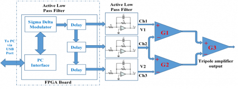
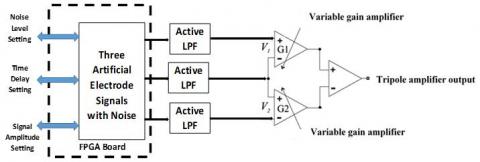
Figure 1 depicts the system's blockdagram design, which is utilized to create a three-channel synthetic TMAP signal from a MEC without additive noise. The multi-channel TMAP generator architecture shown in Figure 1 (a) consists of FPGA Board and active low pass filter. The digital controller for the emulated nerve spike generation system is FPGA-based, and it connects to a desktop PC via USB. The device uses on bit Sigma Delta DAC bit stream sequence that corresponds to the intended nerve activity waveform to operate three channels through active LPF. In order to mimic the impact of the TMAP traveling through the nerve bundle as it passes through the MEC, each channel is time-shifted relative to the preceding channel.
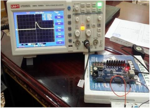
The controller uses a Digilent Basys 2 board that is readily available off the market and has a USB interface. The simulated signal outputs from the Basys 2 are uncommitted digital outputs.
Using a three-stage computational model, we investigated the stimulation recording nerve cuff electrode designs. The model's first stage was a reshaping technique that estimated the locations of the nerve and fibers within the cuff. This model was used in the second stage to calculate the action potentials produced by the nerve cuffs in a tripole amplifiers recognition of the nerve and surrounding tissue. The potentials were then connected to a cable prototype of a mammalian, myelinated axon in the third stage to determine stimulation thresholds for axonal induction in the peripheral nerves trunk.
(a)
(b)
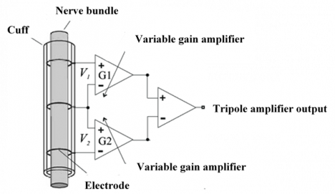
Figure 1. a). Simulated three electrode Cuff with tripole amplifiers; b). Actual three electrode Cuff with tripole amplifiers
2.1 Implementation method
The Xilinx ISE platform is used to synthesis the digital hardware component of the system, which is written in Verilog hardware description language (HDL). Bench testing and modelling is employ the Mentor Graphics ModelSim to simulate and evaluate the design. The sigma delta generator has timing reference is 100 MHz built-in frequency. The sampling frequency of sigma delta is maintained at slightly under 100 kHz (99 kHz, to be precise), which is sufficient for the creation of TMAP signals while maintaining the needed 10 bit data accuracy. Only 30% of the FPGA slices resource are used by the entire system, indicating that more cost reduction would be possible if the design were to be fully implemented in custom CMOS technology.
2.2 Active low pass filter design
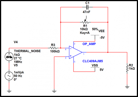
Figure 2 displays active low pass filter using operation amplifier, which is made up of a basic feedback resistance paired with input resistance connected to simple RC filter to lower the amplitude and reject the high frequency range even more. To generate the TMAP waveform, each sigma delta signal is sent via one of these filter for waveform smoothing and gain adjustment.
Figure 2. Active LPF with OP_Amp stage
2.3 Verilog HDL coding
This section presents a brand-new linearized signal generator design strategy based on the segma delta method, which consists of one bit sigma delta modulator and a linearization procedure based on the scrambler technique. In addition, a phase shift register is used to generate a white Gaussian noise and incorporated to the system. The synthesis and design of the entire device throughout implementation on the FPGA board were done using the Verilog HDL. Moreover, this approach gives the researcher freedom to reconfiguration the design using a NAND gats array library for a suitable silicon progression, like the 0.35-m CMOS technology from Austria microsystems that was previously employed.
The typical TMAP pattern given by Eq. (1) [14]:
$V_m(t)= \begin{cases}A t^n e^{-B t} & t \geq 0 \\ 0 & t<0\end{cases}$ (1)
where, A and B are constants and n is an integer (typical values used are A = 4.08x101Vs-1, B = l.5x104s-1 and n = 1).
Additionally, the user may alter the waveform, amplitude, and time period by changing the values of the parameters A, B, and n. This provides the user with various alternatives to switch TMAPs more quickly and easily without having to change the software or hardware architecture. Additionally, a USB interface controller port has been provided in this design to ensure it very simple for the operator to operate the FPGA board using a PC.
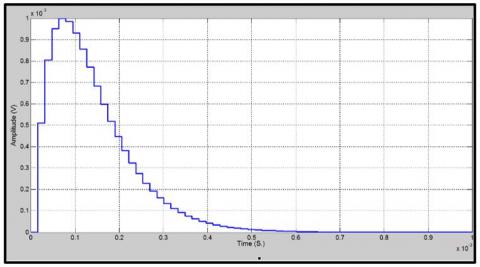
The TMAP function in Eq. (1) has a length of around 0.7 ms, and 64 sample points equate to a sampling frequency is 100k sample/sec., as illustrated in Figure 3.
Figure 3. The template function for TMAP with 64 samples
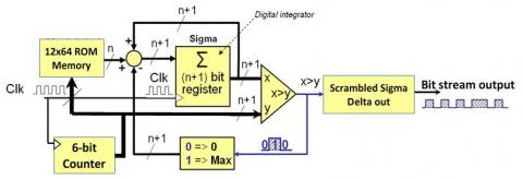
Figure 4. The scrambled sigma delta modulator architecture
The 64 x 12 ROM has been built on the FPGA for representing each sampling of the digital TMAP signal with 12 bit binary value that has been resized to the device output range (3.3V). This value used added to Delta section as input signal with sigma delta feedback signal. The counter is used as memory index value for calling each sample. The Sigma Delta output applied to creambler unit for linearization process and minimizing the voltage ripple of the outputs. The active RC LPF (attenuator) is used for smoothing the waveform as mentioned in the low pass filter design section. The output impedance of the LPF is set to be around 15 kΩ, with a -3dB point at roughly 100 kHz. The electrode cuff prob interface approach recorded the TMAPs generally in a band between roughly 1 Hz and 5 kHz [14], which results in a smooth response into the desired frequency band.
The scrambled Delta Sigma modulator exposed in Figure 4 involve four stages:
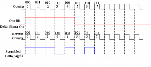
The scrambler in the output simply affects the bit order of output values arrive, each period's duty cycle is divided, or "scrambled," into a number of smaller pulses. To minimize times when all channels are off, the pulses of each channel will work together. scrambler -Sigma-Delta provides 12-bit, which enhances the clarity and sharpness of the waveform. Since the counter cycles through the whole value range that the 12 bit output. The advantage is that it disperses the produced noise to higher frequencies, which are subsequently filtered by the active LPF at the output. Figure 5 the output counting using scrambler-Sigma-Delta and traditional sigma-Delta algorithms are explained in the examples that follow. The output duty cycle remains intact, but the scrambling results provided a very uniform distribution of high and low of the bit stream output across the duration of the sigma delta sequence. The LPF smoothing in this graphic was purposefully chosen to highlight the modification of scrambler sigma delta output approach. In the actual device, the LPF time constant (RC) could ideally be bigger than illustrated below, however this is constrained by the necessity to maintain a high frequencies signal component.
Figure 5. The scrambler-sigma-delta and traditional sigma-delta algorithms
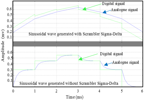
Additional simulations with Matlab Simulink have already been utilized to confirm the behaviour of the system algorithm as shown in Figure 6. In this simulation, the RC smoothing has been used to show how the output of the scrambled and unscrambled Sigma Delta differs for sinusoidal wave. The simulation plot clearly displays the results of each stage in addition to the substantial improvement in signal quality at the scrambler's output.
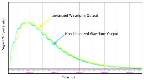
The TMAP waveform may be detected as an analogue signal once the FPGA's Sigma Delta output has been processed by the Active LPF to create it. The low pass filter's capacitor's charging curve is still visible because the sampling frequency is 100 k Sample/s and the LPF's cut-off frequency is 338 Hz. A TMAP signal produced with this method is shown on ModelSim SE 6.3a Simulation trace in Figure 7. The trace clearly shows the ripple associated with RC charging.
Figure 6. Sinusoidal wave generated with and without scrambler sigma-delta
Figure 7. The TMAP waveform ripple with and without linearization method
The scrambling Sigma Delta generator has been altered in order to eliminate voltage ripple in the nerve spike waveform and create a straight line between points for all samples locations. The new module employs the scrambling technique, which distributes the output values of 1 and 0 throughout the whole Sigma Delta period. This enables varying reference magnitude input to be supplied into the output comparison. The reference value is changed to provide a constant voltage difference across the smoothing capacitor's input resistor, which results in a linear change in voltage as shown in Eq. (2):
$V_{\text {out }}=((V i * T p) / T c)+$ Vripple (2)
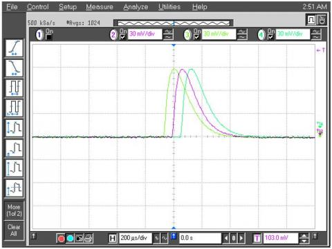
where, Vi is the input voltage and Tp is Active high pulse time period, Tc is the Sigma Delta time period and Vripple is the voltage ripple appear in Vout. Figures 8 and 9 illustrate the linearized ripple that was generated using oscilloscope trace and ModelSim SE 6.3a Simulation respectively.
It is important to note that, from the standpoint of simulation, the addition of delays essentially converts the TMAP function into a propagating wave (AP) (function of time only) with the given MEC's spatial characteristics.
According to Figure 9, every output has a temporal delay in relation to the one before it. The time delay may be precisely determined based on the desired apparent propagation velocity and need not be an integer multiple of the sample delay when using programmable circuitry.
Figure 10 shows the FPGA synthesis of the entire system, which includes a scrambler and a linearization unit. The adjustments weren't expensive in terms of additional logic gates and were integrated into same FPGA board as the nerve spik generator.
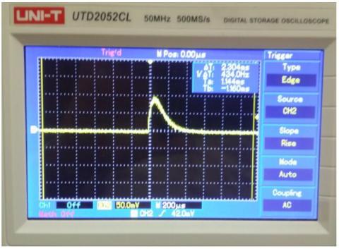
Figure 8. Oscilloscope trace output three channels outputs for the system after linearization
Figure 9. ModelSim SE 6.3a Simulation three channels outputs for the system after linearization
Figure 10. The completed configuration system with linearization modification
Additionally, employing one bit Sigma-Delta rather than multiple bits reduces the number of FPGA I/O ports needed for the design. The most significant performance for this system is the ability to build short delay time for high speed nerve spike such as 100 m/s.
Therefore, using a different strategy with the same hardware size would make doing these features is difficult. Furthermore, this linearization approach works with various signal processing methods as well as sigma delta, including one-bit sigma delta modulators, with relative ease.
A background noise is added for each channel for further performance improvement to the system to be more accurate and useful for different testing cases.
This technique is being developed to increase the signal waveform's accuracy while keeping the hardware's complexity and size constant. The FPGA board is organised via a USB port, making it simple to change the noise ratio (SNR), conduction velocity, and TMAPs waveforms.
A Linear Feedback Shift Registers (LFSRs), is a common technique for producing a one-bit bit stream of random digital output for white Gaussian noise generator.
The only additional hardware required for a shift register to produce binary random numbers is programmable clock dividers, three exclusive-OR gates, and three shift registers. The output of the LFSR has a level shifter attached to it to map the ones to VDD and zeros to -VDD in order to eliminate the DC offset and get a roughly zero mean output [9]. The level shifter's output is pass through the active LPF, as seen in Figure 11.
Figure 11. Block diagram of the simulated TMAP system with white Gaussian noise
The three-channel system's circuit schematic is shown in Figure 11. It is intended to provide uncorrelated white noise for each unique TMAP signal in order to imitate the actual conditions of each electrode in the actual experimental setting. The necessary adjustable noise sources are provided via three sets of taps and an eight bit noise level input.
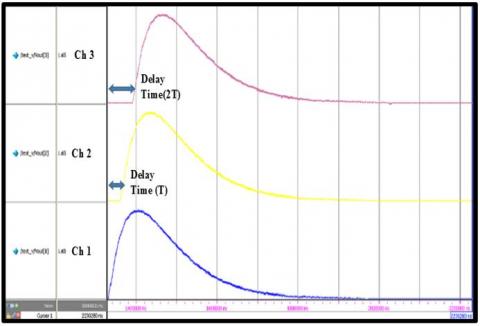
The analogue TMAP signals are combined with a different, uncorrelated noise source for each signal as the process of signal synthesis comes to a close. The TMAP signal and noise are combined to complete this stage, as demonstrated in oscilloscope traces in Figure 12.
The capability of this method to imitate extremely high TMAP with propagation velocities as high as 100 m/s is by far its greatest benefit. With regard to the conduction velocity, this offers a very broad range of data that may be gathered for testing and evaluation of the VSR at very small step. Moreover, this design minimize hardware, and expensive as demonstrated in Table 1.
Figure 12. The Oscilloscope traces of TMAP signals with noise
Table 1. Xilinx Spartan 3E utilisation summary
|
Device Utilization Summary |
|||
|
Logic Utilization |
Used |
Available |
Utilization |
|
Number of Slice Flip Flops |
30 |
1,920 |
1% |
|
Number of 4 input LUTs |
550 |
1,920 |
28% |
|
Number of occupied Slices |
300 |
960 |
31% |
|
Number of Slices containing only related logic |
300 |
343 |
87% |
|
Number of Slices containing unrelated logic |
0 |
343 |
0% |
|
Total Number of 4 input LUTs |
557 |
1,920 |
29% |
|
Number used as logic |
30 |
|
|
|
Number used as a route-thru |
15 |
|
|
|
Number used as Shift registers |
500 |
|
|
|
Number of bonded IOBs |
5 |
83 |
6% |
|
IOB Flip Flops |
1 |
|
|
|
Number of BUFGMUXs |
1 |
24 |
4% |
|
Average Fanout of Non-Clock Nets |
1.2 |
|
|
Table 2. Equivalent gate counts and power consumption data for each approach
|
Method |
Power Consumption |
|
Scrambler Delta_Segma Method |
Consumed total gate number: 953,177 |
|
Consumed current: 19 mA |
|
|
Consumed Power(measured):21.5 mW |
|
|
Consumed Power(measured):21.23 mW |
|
|
Traditional Deltad_Segma Method |
Consumed total gate number: 1,012,112 |
|
Consumed current: 38 mA |
|
|
Consumed Power(measured):32.2 mW |
|
|
Consumed Power(measured):31.85 mW |
Table 2 displays the device's total power consumption as well as the measured and anticipated power usage for each strategy. The results show the traditional Sigma Delta technique used around 10% more FPGA resources compare with proposed method in both terms gates number and power consumption. Keep in mind that the design is executed on an FPGA when looking at the power consumption numbers. It is common knowledge that an FPGA configuration will consume a lot more power than a comparable bespoke device of the kind needed in an implanted system. Moreover, the select of CMOS technology for configuration the system would lead for significant impact on consumed power and hardware.
This paper describes a device that can produce three-channel TMAP that accurately and flexibly simulates the output of a three-electoral cuff. The system created by scrambled one bit Sigma Delta DAC is used in the suggested strategy. The system is essentially produced three synthetic TMAPs with time delay and adjustable white noise for tripole amplifier test. The employment of scrambling Sigma Delta-based approaches delivers the major benefits, such as high speed and accuracy data and the integrity, while minimizing the hardware complexity and price.
An innovative technique to enhance the frequency response of a smoothed Sigma Delta output is provided by the linearisation module of the Sigma Delta process is suggested, and is useful in many other applications. The trick to making this alteration possible is the FPGA's adaptability. A USB interface input/output port makes it simple to change the TMAP pattern. The device can synthesize TMAPs with propagation velocities ranging from around 1 to 120 meters per second in increments of 1 meter per second. Furthermore, uncorrelated white Gaussian signals that are simple to manipulate using input user controller have been included to each channel. Three channel of artificial electrode cuff signals have been successfully tested using the synthesizer. This system supplies the artificial TMAP to the tripole amplifier configuration for velocity selective recording approach application test.
In this paper, one bit DAC is designed; in the future, a Delta sigma based DAC could be implemented for TMAP evaluating instead of use basic DAC, this will boost the real time recording performance.
The approach shown here enables extensive testing without the moral and financial drawbacks of using animals in experiments. However, keep in mind that the synthesized signals are obtained from this system approximation cannot replace the human nerve test for validation carried out for laboratory studies.
The Sigma-Delta DAC has high accuracy and low ripple voltage, make it ideal for TMAP recording applications. The sigma-delta modulator, a special single-bit scrambler sigma-delta DAC generates signals with a predetermined recurrence frequency. While the repetition rate is constant, the output signal is resistant to non-linear inter-symbol interference. As a result, the system is robust and the converter has a good out-of-band noise and ripple reduction.
Consequence, the converter has excellent responsiveness and strong matching capabilities while also having high noise reduction and ripple, resistance to clock instability, and other error causes that are typically present in 1-bit converters.
The single bit sigma-delta modulator is the optimum solution for designing the artificial nerve spike signal for pre-processing for in front end tripole amplifiers in three electrode cuffs.
The author would like to express his sincere gratitude to the Biomedical Engineering Department, College of Engineering, University of Thi-Qar for providing the equipment and tools essential to conduct the tests of the study.
[1] Schuettler, M., Seetohul, V., Taylor, J., Donaldson, N. (2006). Velocity-selective recording from frog nerve using a multi-contact cuff electrode. Engineering in Medicine and Biology Society, 28th Annual International Conference of the IEEE, 1: 2962-2965. https://doi.org/10.1109/IEMBS.2006.260335
[2] Taylor, J., Schuettler, M., Clarke, C., Donaldson, N. (2012). The theory of velocity selective neural recording: a study based on simulation. Medical & Biological Engineering & Computing, 50(3): 309-318. https://doi.org/10.1007/s11517-012-0874-z
[3] Clarke, C.T., Xu, X., Rieger, R., Taylor, J., Donaldson, N. (2008). An implanted system for multi-site nerve cuff-based ENG recording using velocity selectivity. Analog Integrated Circuits and Signal Processing, 58(2): 91-104. https://doi.org/10.1007/s10470-008-9233-2
[4] Andreasen, L.N.S., Struijk, J.J., Haugland, M. (1997). An artificial nerve fiber for evaluation of nerve cuff electrodes. Proceedings of the 19th Annual International Conference of the IEEE, Chicago, IL, USA, pp. 1997-1999. https://doi.org/10.1109/IEMBS.1997.758734
[5] Sheu, Y.H., Chenb, C.W., Weyb, T.S. (2004). The development of multi-channel action-potential generator for testing neurophysiologic data acquisition/analysis system. 11th International Conference on Biomedical Engineering (ICBME), pp. 17-20. https://doi.org/10.1109/BIOCAS.2004.1454121
[6] Shehata, K.A., Aboul-Dahab, M.A., El-Ramly, S.H., Hamouda, K.A. (2008). An FPGA based 1-bit all digital transmitter employing Delta-Sigma Modulation with RF output for SDR. 2008 2nd International Conference on Signals, Circuits and Systems, pp. 1-6. https://doi.org/10.1109/ICSCS.2008.4746928
[7] Hongzhi, S., Jie, W., Yichao, M., Yang, K., Jie, Z. (2009). A FPGA-based 7-order 1-bit sigma-delta modulator for high-precision signal generation. 2009 9th International Conference on Electronic Measurement & Instruments, pp. 160-164. https://doi.org/10.1109/ICEMI.2009.5274097
[8] Kiss, P., Arias, J., Li, D., Boccuzzi, V. (2004). Stable high-order delta–sigma digital-to-analog converters. IEEE Transactions on Circuits and Systems I: Regular Papers, 51(1): 200-205. https://doi.org/10.1109/TCSI.2003.821283
[9] Aouini, S., Roberts, G. (2006). A predictable robust fully programmable analog gaussian noise source for mixed-signal/digital ATE. 2006 IEEE International Test Conference, pp. 1-10. https://doi.org/10.1109/TEST.2006.297677
[10] Al-Shueli, A., Clarke, C.T., Taylor, J.T. (2012). Simulated nerve signal generation for multi-electrode cuff system testing. 2012 International Conference on Biomedical Engineering and Biotechnology, Macau, Macao, pp. 892-896. https://doi.org/10.1109/iCBEB.2012.354
[11] Al-Shueli, A.I. (2013). Signal processing for advanced neural recording systems. PhD Thesis, University of Bath, Bath, UK.
[12] Tan, Z., Chen, C.H., Chae, Y., Temes, G.C. (2020) Incremental delta-sigma ADCs: A tutorial review. IEEE Transactions on Circuits and Systems I: Regular Papers, 67(12): 4161-4173. https://doi.org/10.1109/TCSI.2020.3033458
[13] Jang, M., Lee, C., Chae, Y. (2019). Analysis and design of low-power continuous-time delta-sigma modulator using negative-R assisted integrator. IEEE J. Solid-State Circuits, 54(1): 277-287. https://doi.org/10.1109/JSSC.2018.2871111
[14] Taylor, J., Donaldson, N., Winter, J. (2004). Multiple-electrode nerve cuffs for low-velocity and velocity-selective neural recording. Medical and Biological Engineering and Computing, 42(5): 634-643. https://doi.org/10.1007/BF02347545