Noora Nazar*![]() | Qusay Al-Doori
| Qusay Al-Doori![]() | Omar Alani
| Omar Alani![]()
© 2023 IIETA. This article is published by IIETA and is licensed under the CC BY 4.0 license (http://creativecommons.org/licenses/by/4.0/).
OPEN ACCESS
Low-Density Parity Check (LDPC) codes are viewed as one of the best error correction coding (ECC) methods in terms of correction efficiency. They have been used in several modern data transmission standards, where the codecs are often built inside specialized integrated circuits (ICs). On the other hand, Complementary Metal-Oxide-Semiconductor (CMOS) circuits have evolved as a critical design characteristic that the designer must consider such as power, which has been overlooked by many researchers. For that reason, in this paper, a research work that reduces LDPC encoder power consumption is presented using a well-known power reduction method named Dynamic Voltage and Frequency Scaling (DVFS), which is one of the most powerful power reduction strategies in CMOS circuits. The proposed system includes a fuzzy logic controller with the DVFS technique to control and select the optimum level of voltage that enters the encoder to reduce its total power consumption. This combination of these two techniques showed significant power reduction and control while causing no impact on the LDPC efficiency, flexibility, and performance. Comparisons with other studies covering power reduction in LDPC codes have shown that the purposed system has the best performance over similar systems in the literature.
Forward Error Correction (FEC), Automatic Repeat Request (ARQ), Low-Density Parity Checks Code (LDPC), Dynamic Voltage and Frequency Scaling (DVFS), Fuzzy Logic Controller
In today's world, digital communication via phones and computers is essential because all messages, data, and information are digital, electronic, and ready to use and share. This information can be stolen or corrupted, posing a serious problem for sensitive and vital industries such as banking. In today's digital age, the security system for accurate and error-free data transmission and reception has become critical, and telecommunications providers and even cellular carriers are competing to develop a fast, power-efficient, and accurate system.
Forward Error Correction (FEC) and Automatic Repeat Request (ARQ) are two ways that can be utilized in the communication channel to fix and reduce errors through signal transmission. FEC codes can secure information and data that leave the transmitter, whether a mobile phone or a personal computer and travel to the base station, then to the receiving device, through a communication path that is directly subject to noise. In addition, unlike ARQ, FEC can detect and correct faults without requiring an Acknowledgement (ACK) from the receiver. This correction could happen if channel coding is used, which adds extra repeated bits at the tail of the transmitted signal. A decoder at the receiver utilizes these bits to determine whether the message is accurate or not and to correct errors [1].
One of the strong FEC codes is the Low-Density Parity Check (LDPC) code. Where Gallager [2] proposed the approach in his PhD thesis half a century ago, but they were forgotten because of the lag of knowledge in computer and communication technology until Mackay and Neal rediscovered them [3]. They showed that long LDPC codes enable a performance error correction only a fraction of a decibel away from the Shannon limit [4]. Therefore, LDPC is chosen for several standards designed for various applications. Perhaps the most common LDPC usage in Wi-Fi [1], DVB-S2 [5], IEEE 802.11n, 802.3an, 802.16a, Wi-MAX, and other communication standards [6-8].
LDPC codes can provide efficient encoding, fast decoding, low latency, and the best amount of error floors with robust error detection and correction capabilities and do not require as much interleaving to achieve good error performance as turbo codes [9]. These codes can be represented by a parity check matrix (PCM) H or a tanner graph, essentially a bipartite graph intended to illustrate LDPC graphically. There are various classifications for LDPC based on its PCM content, such as binary and non-binary or regular and irregular, as shown in Figure 1.
With a wide variety of strategies for reducing energy usage specialized for microprocessors and Complementary Metal-Oxide-Semiconductor (CMOS) circuits such as energy gating (shutdown) [10], clock gating method (sleep mood) [11], and Dynamic Voltage and Frequency Scaling (DVFS) [12], Attempting to integrate these technologies with networking is an attractive manner. This paper aims to implement DVFS on the LDPC circuit so that the power consumption of the LDPC circuit is minimized regardless of the frequency used and the communication standard. This can help in preserving longer battery life. Such a working area was not considered in previous research, and the design is done by establishing an appropriate mathematical model that uses frequency to reduce the voltage and later the power of the LDPC encoder without affecting its performance, where this notion can be used to support next-generation digital communication requirements and broader network applications. The results of the proposed system show a significant power reduction of 90% for the medium frequency range from 100MHZ to 1GHZ.
This paper is organized as follows: section 2 will look briefly through the literature, while section 3 will represent the implementation of the LDPC encoder and its specifications. Section 4 will purpose power measurement for the LDPC encoder logic circuit. Following that, section 5 will show the proposed power controller system, and section 6 has the results of previously mentioned designs along with comparisons related to different power reduction designs. Lastly, section 7 will present the conclusion.
Figure 1. LDPC representation as PCM and tanner graph [1]
Tremendous research on LDPC codes has been done in the literature. It has been observed that numerous encoding methods for LDPC codes have been established, such as [13-17], In addition to the developments in decoding on several aspects such as research [18-20] and in LDPC power conservation in specific such as researches [21-25] which is the primary goals for 5th generation (5G) and 6th generation (6G) wireless communications besides reliability, efficiency, and latency [26-28]. For example, the authors Nguyen et al. [15] presented a novel efficient encoding method and a high-throughput low-complexity encoder architecture for quasi-cyclic LDPC (QC-LDPC) codes for the 5th-generation (5G) New Radio (NR) standard. In addition, the authors Nandalal and Anand Kumar [29] presented an efficient compact encoding process with the pipelining design of an LDPC Encoder with two-stage, three-stage, and Maximal Rate Pipelining (MRP) structures. While the author’s Tian et al. [30] investigated the parallel design and implementation of the 5G QC-LDPC encoder. Furthermore, the study presented by Petrović et al. [31] proposes a novel partially parallel architecture that can provide high Hardware Usage Efficiency (HUE) while achieving LDPC encoder flexibility and support for all 5G NR codes. On the other hand, the authors Hyla et al. [32] presented a research work that shows that the LDPC coding scheme can also be applied in a system characterized by highly limited computational resources. Table 1 focuses on those modern encoder power reduction techniques with advanced details such as LDPC type and the algorithm used, power reduction method used, application, improvement scope, and drawbacks.
Table 1. Related work overview
|
Ref. No. |
Year |
LDPC Type |
LDPC Encoder Algorithm Used |
Power Reduction Method |
Application |
Improvement Scope |
Drawbacks |
|
[15] |
2019 |
QC-LDPC |
Richardson–Urbanke (RU) Method |
Storing the quantized value of the permutation information for each submatrix instead of the whole parity check matrix. |
The hardware implementation is based on TSMC 65-nm CMOS technology suitable for 5G-NR requirements. |
High-Throughput Low-Complexity and Flexible Parallel Encoder Architecture can reduce power consumption. |
A full-base matrix can cause the encoding of extra code bits, which wastes resources and power on the transmitter. |
|
[29] |
2021 |
Binary LDPC |
Straightforward Encoding with Generator Matrix Multiplication |
Pipelining design of the LDPC Encoder with a two-stage, three-stage, and Maximal Rate Pipelining (MRP) structures. |
XC3S-250E FPGA Device |
Reduce Overheads Such as Power and Area with Less Memory usage. |
The algorithm must be modified to work with a larger matrix dimension. |
|
[30] |
2021 |
QC-LDPC |
High parallelism encoding algorithms |
The QC-LDPC encoder employs a multi-channel parallel structure to obtain multiple parity check bits. |
The hardware implementation is based on SIMC 28 nm CMOS technology suitable for 5G-NR requirements. |
Higher throughput, lower encoding latency, flexibility, coding efficiency, and hardware power consumption are suitable for 5G eMBB and URLLC scenarios. |
The algorithm can be adjusted to operate with lesser CMOS technology, and the design may suffer from slightly high complexity. |
|
[31] |
2021 |
Binary LDPC |
Forward substitution-based encoding |
Partially parallel architecture. |
5G-NR |
High throughput, low latency, best hardware usage efficiency (HUE), and more energy-efficient encoder design. |
The coding delay has not reached the minimum compared to the study [15]. |
|
[32] |
2022 |
QC-LDPC |
Richardson–Urbanke (RU) |
Appling LDPC in microcontroller with limited computational resources. |
IoT |
Throughput is raised while encoding time is lowered, reducing energy use and improving error correction. |
The algorithm can be adjusted to operate with alternative power reduction techniques, and no complexity or flexibility statistics are provided. |
Depending on the data in Table 1, Focusing on reducing LDPC power consumption is overlooked in many pieces of research, and all of the mentioned methods strive to develop a specific parameter and treat power consumption as a secondary parameter rather than attempting to address it the power problem on its own. This paper's work focuses on power only by employing a DVFS power reduction technique to reduce LDPC encoder power consumption. This concept can be utilized to meet next-generation digital communication demands and more comprehensive network applications by designing an acceptable model that achieves the required power reductions for the LDPC encoder without risking its performance.
The digital communication system worldwide consists of 9 steps to transfer a message from its digital source to the end user as shown in Figure 2. The medium that is responsible for transferring a message is a channel which is known as a non-dependent medium because it is affected by noise that can affect the content of the message. LDPC codes are channel encoders and decoders [33] located at the transmitter side and the receiver side of the communication channel. The encoder's job is to add additional parity bits that are linked randomly to the transmitted message bits. This random link can ensure the correct correction for more than one bit in fault message by the decoder at the receiver side without the need for retransmission or handshaking [9, 34].
Figure 2. Channel encoding and decoding demonstration
For example, if we want to transmit a message 1011 the LDPC encoder will create additional bits added to the original message before transfer so the final message or code word to be transmitted will be 1011100.
This work uses the Straightforward encoding with the generator matrix multiplication encoder method because when the generator matrix is pre-calculated, the required matrix multiplication for specific codes can be efficiently achieved in hardware [31, 35]. The implementation of the LDPC Encoder is described briefly in the following steps:
Step 1: The H matrix is constructed randomly, this work uses a binary irregular matrix with size 4*7, and the coding rate, which is the ratio between message bits and parity bits, is equal to 0.5.
Step 2: a shifting for all rows of the H matrix is done, and then the Gaussian elimination is applied. After this step, the G matrix will be constructed and contain two parts that can be noticed as shown in Eq. (1) [36]:
$G=\left[I_{n-k}: P_{n-k}\right]$ (1)
I: is the identity part, and P: is the parity part.
Step 3: a 4-bits message is entered.
Step 4: code word is calculated by Eq. (2) [31]:
Code word =Message * G matrix (2)
When the identity part of the G matrix is multiplied by the message bits, the result will be the same message bits. Therefore, when the message bits are multiplied by the parity part in the G matrix, this will result in the three parity bits (p1 p2 p3), which can explain the code rate value of 0.5. Figure 3 is a flowchart for constructing the encoder. The specifications of the design are demonstrated in Table 2.
Table 2. Specifications of LDPC encoder design using MATLAB M. file
|
Parameter |
Specification |
|
Type of LDPC PCM matrix |
Binary irregular |
|
Algorithm used |
Straightforward encoding with generator matrix multiplication. |
|
Size of H matrix |
4×7 |
|
Number of message bits |
4 bits |
|
Number of parity bits |
3 bits |
|
Number of code word bits |
7 bits |
|
Code rate |
4/7=0.5 |
Figure 3. LDPC encoder flowchart
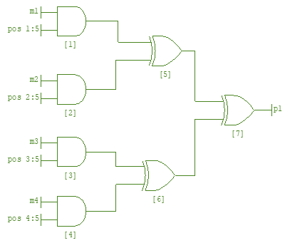
The multiplication operation that generates the code word is the primary stone for designing the logic circuit for the LDPC encoder. As a result, following the design steps of previous studies [37-40], it can be noticed that multiplication is represented by a logical AND gate, and a logical XOR gate represents module-2 addition. Figure 4 demonstrates the initial encoder logic circuit for only generating the first parity bit (p1). The other parity bits (p2, p3) will follow the same design patron but with different matrix positions.
Figure 4. The initial LDPC encoder logic circuit for the first parity bit p1. The first inputs (m1, m2, m3, m4) represent the message bits, and the second inputs (pos 1,5, pos 2,5, pos 3,5, pos 4,5) represent the position in the G matrix
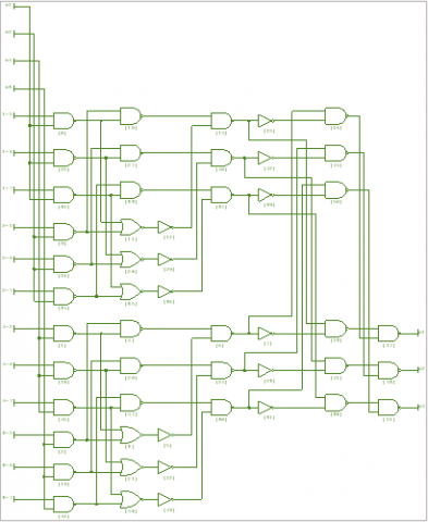
To simulate the behavior of these digital circuits on a Very Large Scale Integration Circuit (VLSI), all gates in the previous design were changed to NAND, NOR, NOT logic gates. In other words, In IC fabrication, there are no XOR or AND logic gates. Only NAND, NOR, and NOT gates are used [41], as demonstrated in Figure 5.
Figure 5. Final LDPC encoder logic circuit
From the above logic circuit, fan-out and path values can be calculated. In this work, the fan-out of the above circuit will be calculated by looking at each gate fork. The number of forks for a specific gate is the fan-out for that gate, as shown in Table 3. On the other hand, the path will be calculated by looking at each output gate individually, and the number of gates connected to the main output gate is the circuit path [42].
Table 3. fan-out of LDPC encoder logic circuit
|
Gate no. |
1 |
2 |
3 |
4 |
5 |
6 |
7 |
8 |
9 |
10 |
11 |
12 |
13 |
14 |
15 |
16 |
17 |
|
No. of output |
2 |
2 |
1 |
1 |
1 |
2 |
1 |
2 |
2 |
1 |
1 |
1 |
2 |
1 |
1 |
1 |
1 |
|
Gate no. |
18 |
19 |
20 |
21 |
22 |
23 |
24 |
25 |
26 |
27 |
28 |
29 |
30 |
31 |
32 |
33 |
34 |
|
No. of output |
2 |
2 |
1 |
1 |
1 |
2 |
1 |
2 |
2 |
1 |
1 |
1 |
2 |
1 |
1 |
1 |
1 |
|
Gate no. |
35 |
36 |
37 |
38 |
39 |
40 |
41 |
42 |
43 |
44 |
45 |
46 |
47 |
48 |
49 |
50 |
51 |
|
No. of output |
2 |
2 |
1 |
1 |
1 |
2 |
1 |
2 |
2 |
1 |
1 |
1 |
2 |
1 |
1 |
1 |
1 |
Table 4. Specifications of LDPC encoder logic circuit
|
Parameter |
Specification |
|
Total number of inputs |
16 |
|
Total number of output |
3 (p1,p2,p3) |
|
Total number of gates |
51 |
|
Total number of paths |
16 paths for each output. total=48 |
|
Maximum gate output |
2 |
|
Maximum path gates |
7 gates |
There are multiple possible paths in the circuit, and each one gives a time delay. The worst case scenario that gives the maximum time delay is related to the longest path, which is for P1 is path16= [gate17, gate16, gate15, gate13, gate12, gate11, gate9] for P2 is path16= [gate34, gate33, gate32, gate30, gate29, gate28, gate26] and for P3 is path16= [gate51, gate50, gate49, gate47, gate46, gate45, gate43]. Specifications for the LDPC logic circuit are shown in Table 4.
In general, each logic gate has a time delay. If its value increases, this will also increase the frequency needed for the circuit so that the voltage requirement will be increased, resulting in power dissipation in the overall circuit [42-44]. Furthermore, the circuit delay time is the sum of all the gate delays through which the input will propagate to the output. The gate timing delay (td) is given as [45]:
$t_d=\frac{C_L V_{d d}}{\mu C_{o x} \frac{w}{l}\left(V_{d d}-V_{t h}\right)^2}$ (3)
where, CL is the load capacitor for each gate, μ is the carrier mobility, Cox is the oxide capacitance, $\frac{w}{l}$ is the transistor width-to-length ratio, and Vth is the threshold voltage. Cox is given by the study [45]:
$C_{o x}=\frac{\varepsilon_{o x}}{T_{o x}}$ (4)
where, tox is the oxide thickness and ϵox is the oxide permittivity. For silicon devices, ϵox = (3.9)(8.85 × 10⁻¹⁴) F/cm.
Also, the parameter used in the design Ki is called the trans-conduction parameter for the i-channel device. Where i is either the p or n substrate. For simplicity, it is referred to as the conduction parameter, which for an i-channel device is given by the study [43]:
$K_i=\frac{W \mu_i C_{o x}}{2 L}$ (5)
As Eq. (5) indicates, the conduction parameter is a function of electrical and geometric parameters. The oxide capacitance and carrier mobility are constants for a given fabrication technology. However, the geometry, or width-to-length ratio w/l, is a variable in the design of Metal Oxide Silicon Field Effect Transistors (MOSFETs) used to produce specific current-voltage characteristics in MOSFET circuits.
Figure 6. Time delay measurement MATLAB M. file code for LDPC encoder circuit
In addition to previous parameters, fan-out and path values obtained from the circuit in Figure 4 are used, a time delay for each logic gate in the LDPC encoder circuit can be measured, and a flowchart for calculating it is shown in Figure 6.
The used power measurement system parameters are listed in Table 5.
Table 5. Specifications of the proposed LDPC encoder power measurement system
|
Parameter |
Specification |
|
Range of voltages |
[0.8-3.5] Volt |
|
Range of frequencies |
[10-900] MHz |
|
CMOS technology |
16 nm |
|
Technology parameters [46-48] |
CL: 1.78×10⁻¹⁴ COX: 0.028 Wn: 1.76×10⁻⁸ Ln: 1.76×10⁻⁸ Wp: 1.76×10⁻⁸ Lp: 1.76×10⁻⁸ µp: 0.0075 µn: 0.028 Vtp: -0.6862 Vtn.:0. 68191 |
|
Energy initialization |
0 |
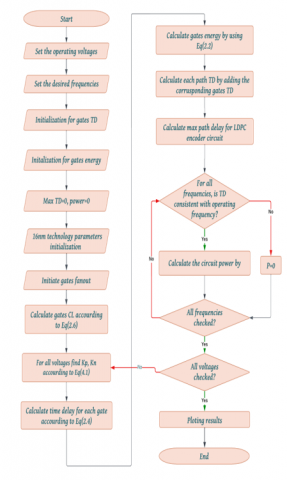
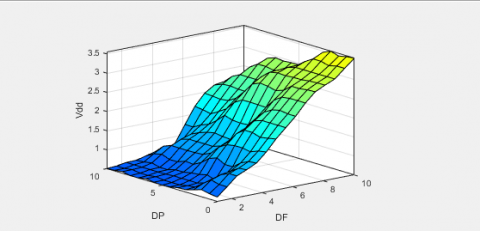
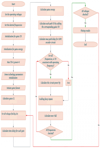
The Fuzzy controller was selected as a controller because it is simple to use and does not need the creation of a mathematical model of the controlling system [41, 49]. The Fuzzy Logic Controller (FLC) controls the voltage in the proposed design. It consists of two inputs, namely frequency and power, and one output Vdd as shown in Figure 7. Several rules can be obtained using these parameters to get the surface in Figure 8. System design steps are demonstrated in Figure 9.
Figure 7. Power controller for the LDPC encoder
Figure 8. The surface of fuzzy used
Figure 9. Flowchart of power reduction for LDPC encoder program
The results of all the mentioned design steps are done using the MATLAB M. file. The result of the system in Figure 6 is shown below:
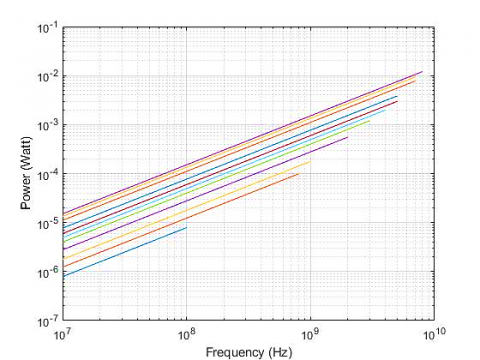
Figure 10. The result of measuring the time delay for each gate in the LDPC encoder circuit. The relationship between two parameters (power and frequency)
As previously stated, each logic gate has a time delay. As a result, lines between power and frequency, as shown in Figure 10, are trimmed at the end because frequency values exceed the circuit's time delay. Therefore, any other result following the trimming point is an error and a waste of energy. Hence it is not counted for and is assumed to be zero. As illustrated in the condition below:
If frequency $>\frac{1}{\text { time delay }}$ then power $=0$
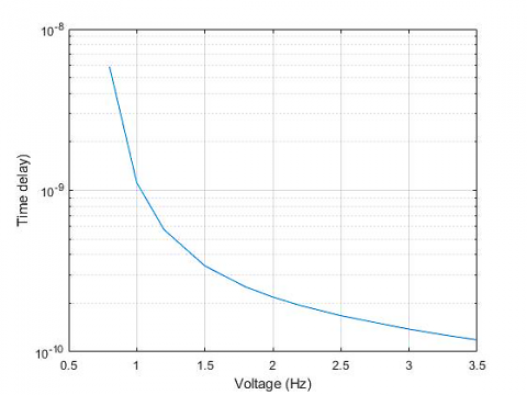
Figure 11. The nonlinear relationship between time delay and voltage for LDPC encoder gates
Figure 12. The relationship between power versus frequency and voltage versus frequency
Figure 13. The relationship between time delay versus voltage
Figure 14. The relationship between power versus frequency and voltage versus frequency
Figure 15. The relationship between time delay versus voltage
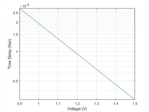
In Figure 11, the nonlinear relationship between time delay and voltage is evident according to Eq. (3). The results of the system in Figure 9 are shown.
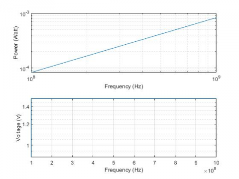
Figure 12 shows a direct relation between voltage and frequency; as frequency grows, so does the voltage, resulting in more power consumption over time. While Figure 13 displays the indirect relation between voltage and time delay, as frequency increases, the delay decreases, resulting in increased voltage and higher power consumption.
A fuzzy controller and DVFS technique were able to manage the voltage inside the system for power savings goals, and the results without the fuzzy controller in Figures 14 and 15, shows that the voltage will increase suddenly as the system starts to work, leading to high power consumption at the beginning of the system function. It good to know that voltage for both figures was fixed to 1.5v.
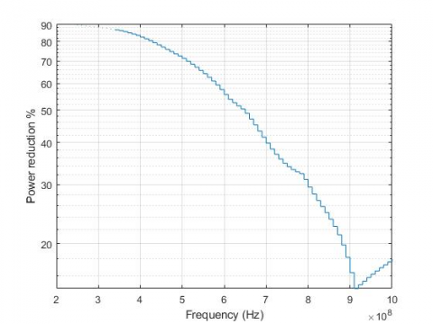
Figure 16. Effect of the controller on the purposed system
Figure 16 depicts the percentage reduction of power when comparing the LDPC circuit with DVFS with the same circuit but without DVFS. It is clear that as the frequency increases, the percentage of reduction decreases. This behaviour is because the frequency is directly proportional to the power, so increasing the frequency will increase power consumption in both circuits with and without DVFS. It is noted that the minimum power reduction is in the 900 MHZ point, in which the reduction was calculated to be 14.5%.
This work is compared with related works mentioned in Table 1. As a result, Table 6 intended to show differences and improvements related to power consumption:
Table 6. Differences between other related works and the proposed method
|
Reference no. |
The method used to reduce power |
Our proposed power manager |
|
[15] |
RU algorithm was used, which is effective in various manners, but using a full-base matrix can cause the encoding of extra code bits, which is a waste of resources and power on the transmitter. Furthermore, the CMOS technology used is 65nm. |
No encoding for extra bits, and our technology is 16nm. Generally, the lower the technology used, the less power is consumed [41]. |
|
[29] |
It offers pipeline usage that can be effective but sometimes suffer from complexity overheads. In addition, the algorithm must be modified to work with a larger matrix dimension. |
Our algorithm is fixable and can work with large matrix dimensions. |
|
[30] |
The author uses 28nm CMOS technology. |
Our method uses 16nm, leading to more power reduction with fewer complexity overheads. |
|
[31] |
Used partially parallel architecture, but it can suffer from coding delay. |
In the proposed algorithm, the effectiveness of the LDPC encoder is managed with less time delay. |
|
[32] |
The system was designed with limited resources, which may limit the performance of the LDPC, and the overall design could have some flexibility overheads. |
In the proposed design, the performance and effectiveness of the LDPC were conserved. |
This study demonstrates that LDPC plays a critical part in communication as a channel encoder and decoder. Power management entity is critical in today's communication systems since every circuit must handle the power consumption issue, for both handheld devices seeking more extended battery life and high-end circuits to avoid too complex cooling packages and reliability difficulties. As proven in the proposed system, combining one of the most potent FEC methods (LDPC) with the essential power manager technique (DVFS) resulted in significant power savings of up to 90% in medium frequency ranges. Also, the fuzzy logic controller has significantly improved the system power consumption by managing the level of voltage that supplies the system and by that LDPC will be a strong candidate for a future communication system with low power and efficient error correction.
This work can be stretched in the future to include studying the power dissipation in the decoder circuit of the LDPC and using another encoding method for the LDPC or managing its power consumption.
[1] Shao, S., Hailes, P., Wang, T.Y., Wu, J.Y., Maunder, R.G., Al-Hashimi, B.M., Hanzo, L. (2019). Survey of turbo, LDPC, and polar decoder ASIC implementations. IEEE Communications Surveys & Tutorials, 21(3): 2309-2333. https://doi.org/10.1109/COMST.2019.2893851
[2] Galleger, R.G. (1962). Low-density parity-check (LDPC) codes. IRE Transactions on Information Theory, 37: 21-28. https://doi.org/10.1109/TIT.1962.1057683
[3] MacKay, D.J.C. (1999). Good error-correcting codes based on very sparse matrices. IEEE Transactions on Information Theory, 45: 399-431. https://doi.org/10.1109/18.748992
[4] Shannon, C.E. (1984). A mathematical theory of communication. The Bell System Technical Journal, 27(3): 379-423. https://doi.org/10.1002/j.1538-7305.1948.tb01338.x
[5] ETSI, E. (2005). Digital video broadcasting (DVB); second generation framing structure, channel coding and modulation systems for broadcasting, interactive services, news gathering and other broadband satellite applications. Part II: S2-Extensions (DVB-S2X), pp. 22-27.
[6] Le, K., Ghaffari, F., Declercq, D., Vasic, B., Winstead, C. (2017). A novel high-throughput, low-complexity bit-flipping decoder for LDPC codes. 2017 International Conference on Advanced Technologies for Communications (ATC), Quy Nhon, Vietnam, pp. 126-131. https://doi.org/10.1109/ATC.2017.8167601
[7] Alabady, S.A. (2018). Binary and non-binary low-density parity-check codes: A survey. International Journal of Information Engineering and Applications, 1(3): 104-117.
[8] Majeed, A.H. (2012). LDPC error floor improvement. Engineering and Technology Journal, 30(3).
[9] Ashou, A.H., Alneema, D.A. (2021). Zynq FPGA implementation of LDPC based on bit flipping algorithm. Journal of Network Communications and Emerging Technologies, 11(8): 1-10.
[10] Kim, H.O., Shin, Y. (2006). Analysis and optimization of gate leakage current of power gating circuits. Asia and South Pacific Conference on Design Automation, 2006, 2006: 565-569. https://doi.org/10.1109/ASPDAC.2006.1594745
[11] Singh, I., Goel, R. (2014). Clock gating: A comprehensive power optimization technique for sequential circuits. https://www.semanticscholar.org/paper/Clock-Gating%3A-A-Comprehensive-Power-Optimization-Singh-Goel/10e01473da0ca87dbdc7666150ca0a08c57d1c75.
[12] Wu, Q., Pedram, M., Wu, X. (2000). Clock-gating and its application to low power design of sequential circuits. IEEE Transactions on Circuits and Systems I: Fundamental Theory and Applications, 47(3): 415-420. https://doi.org/10.1109/81.841927
[13] Andrews, K., Dolinar, S., Thorpe, J. (2005). Encoders for block-circulant LDPC codes. Proceedings. International Symposium on Information Theory, 2005. ISIT 2005, 2005: 2300-2304. https://doi.org/10.1109/ISIT.2005.1523758
[14] Mahdi, A., Kanistras, N., Paliouras, V. (2021). A Multirate fully parallel LDPC encoder for the IEEE 802.11n/ac/ax QC-LDPC codes based on reduced complexity XOR trees. IEEE Transactions on Very Large Scale Integration (VLSI) Systems, 29(1): 51-64. https://doi.org/10.1109/TVLSI.2020.3034046
[15] Nguyen, T.T.B., Tan, T.N., Lee, H. (2019). Efficient QC-LDPC encoder for 5G new radio. Electronics, 8(6): 668. https://doi.org/10.3390/electronics8060668
[16] Richardson, T.J., Urbanke, R.L. (2001). Efficient encoding of low-density parity-check codes. IEEE Transactions on Information Theory, 47(2): 638-656. https://doi.org/10.1109/18.910579
[17] Hocevar, D.E. (2003). Efficient encoding for a family of quasi-cyclic LDPC codes. GLOBECOM '03. IEEE Global Telecommunications Conference (IEEE Cat. No.03CH37489), pp. 3996-4000. https://doi.org/10.1109/GLOCOM.2003.1258979
[18] Harb, H., Chavet, C. (2020). Fully parallel circular-shift rotation network for communication standards. IEEE Transactions on Circuits and Systems II: Express Briefs, 67(12): 3412-3416. https://doi.org/10.1109/GLOCOM.2003.1258979
[19] Addi, S., Berkani, A., Azouaoui, A., Belkasmi, M. (2017). New hard decision decoder of LDPC codes using single bit flipping algorithm. 2017 International Conference on Wireless Networks and Mobile Communications (WINCOM), pp. 2-6. https://doi.org/10.1109/WINCOM.2017.8238191
[20] Català-Pérez, J.M., Lacruz, J.O., García-Herrero, F., Valls, J., Declercq, D. (2019). Second minimum approximation for min-sum decoders suitable for high-rate LDPC codes. Circuits, Systems, and Signal Processing, 38(11): 5068-5080. https://doi.org/10.1007/s00034-019-01107-z
[21] Darabiha, A., Chan Carusone, A., Kschischang, F.R. (2008). Power reduction techniques for LDPC decoders. IEEE Journal of Solid-State Circuits, 43(8): 1835-1845. https://doi.org/10.1109/JSSC.2008.925402
[22] Senthilpari, C., Deena, R., Lini, L. (2022). Low power, less occupying area, and improved speed of a 4-bit router/rerouter circuit for low-density parity-check (LDPC) decoders. F1000Research, 11: 7. https://doi.org/10.12688/f1000research.73404.2
[23] Huang, W., Wang, L. (2020). Low power non-binary LDPC decoder design via adaptive message length control exploiting domain specific information. Journal of Signal Processing Systems, 93(1): 11-23. https://doi.org/10.1007/s11265-020-01533-2
[24] Jin, J., Tsui, C.Y. (2010). An energy-efficient layered decoding architecture for LDPC decoder. IEEE Transactions on Very Large Scale Integration (VLSI) Systems, 18(8): 1185-1195. https://doi.org/10.1109/TVLSI.2008.2007736
[25] Yahya, A., Othman Sidek, M.F., Ali, S. (2009). An efficient encoding-decoding of large girth LDPC codes based on quasi-cyclic. Australian Journal of Basic and Applied Sciences, 3(3): 1734-1739.
[26] Arora, K., Singh, J., Randhawa, Y.S. (2019). A survey on channel coding techniques for 5G wireless networks. Telecommunication Systems, 73(4): 637-663. https://doi.org/10.1007/s11235-019-00630-3
[27] Zhang, Z., Xiao, Y., Ma, Z., Xiao, M., Ding, Z.G., Lei, X.F., Karagiannidis, G.K., Fan, P.Z. (2019). 6G wireless networks: Vision, requirements, architecture, and key technologies. IEEE Vehicular Technology Magazine, 14(3): 28-41. https://doi.org/10.1109/MVT.2019.2921208
[28] Abd Al-Kareem, L.G. (2011). Low-density parity check (Ldpc) codes for a proposed slantlet transform ofdm system in a Rayleigh fading channels with perfect and pilot channel estimation for M_Ary PSK modulation. IJCCCE, 11(2): 65-78.
[29] Nandalal, V., Anand Kumar, V. (2021). Design and analysis of (5, 10) regular LDPC encoder using MRP technique. Wireless Personal Communications, 118(2): 1295-1311. https://doi.org/10.1007/s11277-021-08075-1
[30] Tian, Y.K., Bai, Y., Liu, D.K. (2021). Low-latency QC-LDPC encoder design for 5G NR. Sensors, 21(18): 6266. https://doi.org/10.3390/s21186266
[31] Petrović, V.L., El Mezeni, D.M., Radošević, A. (2021). Flexible 5G new radio LDPC encoder optimized for high hardware usage efficiency. Electronics, 10(9): 1106. https://doi.org/10.3390/electronics10091106
[32] Hyla, J., Sułek, W., Izydorczyk, W., Dziczkowski, L., Filipowski, W. (2022). Efficient LDPC encoder design for IoT-type devices. Applied Sciences, 12(5): 2558. https://doi.org/10.3390/app12052558
[33] Gunnam, K.K. (2006). Area and energy efficient VLSI architectures for low-density parity-check decoders using an on-the-fly computation. Doctoral Dissertation, Texas A&M University, College Station, USA.
[34] Mosleh, M.F. (2011). Evaluation of low-density parity-check codes over various channel types. Engineering and Technology Journal, 29(5): 961-971.
[35] Al-Doori, Q., Alani, O. (2015). A multi polynomial CRC circuit for LTE-Advanced communication standard. 2015 7th Computer Science and Electronic Engineering Conference (CEEC), pp. 19-23. https://doi.org/10.1109/CEEC.2015.7332693
[36] Arora, K., Singh, J., Randhawa, Y.S. (2020). A survey on channel coding techniques for 5G wireless networks. Telecommunication Systems, 73(4): 637-663. https://doi.org/10.1007/s11235-019-00630-3
[37] Fleah, M.A. (2019). Design and implementation of turbo encoder/decoder for digital systems. The University of Technology Control. https://doi.org/10.1109/CAS47993.2019.9075589
[38] Al-doori, Q.F. (2017). Design of a smart power manager for digital communication systems. University of Salford, United Kingdom.
[39] Ashou, A.H., Alneema, D.A. (2021). HLS design of min sum decoding algorithm on Zynq. International Journal of Computer Science and Engineering, 8(7): 10-15. https://doi.org/10.14445/23488387/ijcse-v8i7p102
[40] Abdulsatar, S.M., Saleh, M.A., Abass, A.K., Ali, M.H., Yaseen, M.A. (2021). Bidirectional hybrid optical communication system based on wavelength division multiplexing for outdoor applications. Optical and Quantum Electronics, 53(10). https://doi.org/10.1007/s11082-021-03252-9
[41] Faris, A. (2021). Design and Implementation of an Error Management Scheme for the Pipeline Circuit. M.S. Thesis, University of Technology, Iraq.
[42] Piguet, C. (2018). Low-power CMOS Circuits: Technology, Logic Design and CAD Tools. CRC press.
[43] Khandelwal, P., Brewer, A.J., Minevich, E., Miles, L., Geller, J.I. (2014). Microelectronics: Circuit Analysis and Design. McGraw Hill.
[44] Hussein, R.R.A., Al-Qaraawi, S.M., Croock, M.S. (2020). Viterbi optimization for crime detection and identification. Telkomnika (Telecommunication Computing Electronics Control), 18(5): 2378-2384. http://doi.org/10.12928/telkomnika.v18i5.13398
[45] Jaeger, R.C., Blalock, T.N. (2008). Microelectronic Circuit Design. McGraw-Hill Education.
[46] Balijepalli, A., Sinha, S., Cao, Y. (2007). Compact modelling of carbon nanotube transistor for early stage process-design exploration. Proceedings of the 2007 international symposium on Low power electronics and design (ISLPED '07), pp. 2-7. https://doi.org/10.1145/1283780.1283783
[47] Sinha, S., Yeric, G., Chandra, V., Cline, B., Cao, Y. (2012). Exploring sub-20nm FinFET design with predictive technology models. DAC Design Automation Conference 2012, pp. 283-288. https://doi.org/10.1145/2228360.2228414
[48] Early, S., Exploration, D., Zhao, W., Member, S., Cao, Y. (2006). New generation of predictive technology model for Sub-45 nm early design exploration. IEEE Transactions on Electron Devices, 53(11): 2816-2823. https://doi.org/10.1109/TED.2006.884077
[49] Oleiwi, B.K., Mahfuz, A., Roth, H. (2021). Application of fuzzy logic for collision avoidance of mobile robots in dynamic-indoor environments. 2021 2nd International Conference on Robotics, Electrical and Signal Processing Techniques (ICREST), pp. 131-136. https://doi.org/10.1109/ICREST51555.2021.9331072