Mehdi Ghoumazi* | Mourad Bella | Messaoud Hameurlain
© 2022 IIETA. This article is published by IIETA and is licensed under the CC BY 4.0 license (http://creativecommons.org/licenses/by/4.0/).
OPEN ACCESS
This article focuses on the study of a sensor for the detection of different materials, for which we proposed a novel platform based on 2D photonic crystals. This platform is a nanostructure that carries two parallel waveguides and a resonator in between. For study, this resonator is replaced each time by materials that are: Human Cornea, Teflon (C2F4), Opal (SiO2-nH2O), Aluminum phosphate (Al2PO4) and Topaz (Al2SiO4 (F; OH)2) with their refractive index following, 1.3375, 1.36, 1.45, 1.53 and 1.606 respectively. The proposed design is composed of silicon dielectric rods (Si) with a refractive index of 3.46 submerged in the air where ‘n’ of air is 1. To examine this structure, a PWE (plane wave expansion approach) and FEM (finite element method) are applied. The (PWE) is used to extract the PBG (photonic band gap) and (FEM) used by COMSOL software in order to extract the desired numerical results such as: the distribution of 'n' and the size of the mesh element all along the structure, followed by the behavior of the electric field (E) along the structure at the resonance before and after injection of the different materials. We also presented the variations of the power flow norm, the total energy density as well as the transmission for the materials used. This study allowed us to observe a significant change in the power flow norm and the total energy density as transmission for each material used when their refractive index changes. This change in refractive index 'n' is among the most important parameters in the detection of different types of materials.
photonic crystals, materials, FEM, power flow norm total energy density, sensors
After the contrivance of the optical sensor in 1962 by Clark and Lyons, optical sensing mechanisms have accepted ample attention in the fields of industrial process control, medical diagnostics, military, environmental monitoring, etc. [1, 2] various optical sensors can be implemented using photonic crystal structures [3, 4]. Photonic crystals (PCs) are expected to be a promising platform for sensing. Photonic crystals are periodic arrangement made of various materials that are created to control the propagation of electromagnetic waves [5-7]. By introducing the defects in the photonic crystal structures, many optical components can be realized [8, 9]. In these photonic crystal structures, the periodic modulation of 'n' gives rise to a forbidden region of wavelength (λ) for the propagation of optical waves called PBG (photonic band gap), this is due to the exceptional interest of the PBG. The PBG depends on refractive index (n), rods radius (r) and the lattice constant (a) of the structure [10, 11]. The principle of detection is based on the shift of the resonant wavelength which in turn is due to the change in the refractive index 'n' of the sensor.
From this study, we designed a new nanophotonic structure based on 2D photonic crystals for the detection of five materials. The human cornea refractive index is the first material to be studied, knowing that the average refractive index ‘n’ of the human cornea ranges from 1.335 to 1.4391. The refractive index of the human cornea is one of the determining factors of the refraction and the overall optical properties of the eye, because the change in the refractive index of the cornea can contribute significantly to the overall optical performance of the eye [12] compared to refractive surgery [13]. 1.3375 is the value of the refractive index used in our study. The second material used is Teflon (C2F4); Teflon has interesting properties in the widest temperature range of any polymer up to 250°C. It is insoluble in all common solvents and resists almost all corrosive and acidic materials. It has a very high dielectric resistivity and resistance relative to the other materials, as well as a low dielectric loss [14]. 1.36 is the value of the refractive index of Teflon used. After that, we proposed Opal (SiO2-nH2O) [15, 16] an Opal is a mineral composed of hydrated silica of formula SiO2-nH2O with traces of mg; al; As; U; Fe; Ca; K. It consists of three distinct mineral species, cristobalite, tridymite and hydrated amorphous silica [17]. 1.45 is the value of the refractive index of Opal. Then, we chose Aluminum phosphate (AlPO4) which is commonly used in many human vaccines to stimulate and enhance the immune response against antigens [18, 19]. 1.53 is the value of the refractive index ‘n’ of AlPO4 used in our work. Finally, we investigated Topaz where the most important sources of topaz crystals are found in Brazil, Pakistan, Russia and USA as well as in other parts of the world [20]. Among the main fluorinated minerals we find topaz which comprises a solid solution between two end elements, the first is fluorinated called Al2SiO4F2 (fluorinated topaz) and the second is called hypothetical hydroxyl, Al2SiO4 (OH)2 [21]. 1.606 is the value of the refractive index of Topaz used.
In this study, we presented a design based on two-dimensional photonic crystals (PhC). This design is made up of a square lattice of 35 horizontal dielectric rods and 28 vertical rods submerged in the air. Knowing that the constant of the network "a" is 623 nm and the radius "r" is 0.19 * a. Also, the refractive index "n" of the silicon rods (Si) is 3.46 (εr = 11.9716) and that of air is 1.
The introduction of defects within the structure is leads to the breaking of the PBG. So, the guide modes are allowed to spread within the region. In order to design the desired sensor, different types of point or linear defects are used and the guided modes are regulated by controlling the size and shape of the fault [22].
So, for the calculation of the band diagram, we used the PWE method for photonic crystals (PC). We suppose that the dielectric constant is a periodic function which is written in the following form:
$\varepsilon (r+{{a}_{i}})=\varepsilon (r)(i=1,2,3)$ (1)
Due to the periodicity, we can increase ε-1(r) by a Fourier series. By presenting the elementary reciprocal vectors of the lattice {bi} and the reciprocal vector of the lattice {G}.
${{a}_{i}}\cdot {{b}_{j}}=2\pi {{\delta }_{i,j}}$ (2)
$G={{q}_{1}}{{b}_{1}}+{{q}_{2}}{{b}_{2}}+{{q}_{3}}{{b}_{3}}$ (3)
With {qi} and bi are the arbitrary integers and the primitive reciprocal lattice vectors respectively. As δi,j is the "Kronecker" delta.
${{b}_{1}}=\frac{2\pi }{V}{{\vec{a}}_{2}}\times {{\vec{a}}_{3}},{{b}_{2}}=\frac{2\pi }{V}{{\vec{a}}_{3}}\times {{\vec{a}}_{1}},{{b}_{3}}=\frac{2\pi }{V}{{\vec{a}}_{1}}\times {{\vec{a}}_{2}}$
where, $V=\vec{a}_{1} \cdot \vec{a}_{2} \times \vec{a}_{3}$.
Further ε-1(r) is expressed as:
$\frac{1}{\varepsilon (r)}=\sum\limits_{G}{{{\varepsilon }^{-1}}(G)}\exp (jG.r)$ (4)
where,
${{\varepsilon }^{-1}}(G)=\frac{1}{S}\int{\frac{1}{\varepsilon (r)}\exp (jG.r)}dr$ (5)
In (5), S indicates-the surface of the cell unit, the smallest region, and this perhaps represented the periodic structure.
In the theory of the PWE method it is considered that the electromagnetic wave in materials with the source in free space is zero, linear and time invariant, also the magnetic uniform, μ(r)=1 as well as ε(r) is real in our region.
The Maxwell equation for electromagnetic waves is:
$\left\{ \begin{align} & \vec{\nabla }\times \vec{H}(r,t)=+\frac{\partial \vec{D}(r,t)}{\partial t};\ \nabla \cdot H=0 \\ & \vec{\nabla }\times \vec{E}(r,t)=-\frac{\partial \vec{B}(r,t)}{\partial t};\ \nabla \cdot D=0 \\\end{align} \right.$ (6)
$Knowing\text{ }that:\left\{ \begin{align} & \vec{B}(r,t)={{\mu }_{0}}\mu \vec{H}(r,t) \\ & \vec{D}(r,t)={{\mu }_{0}}\mu \vec{E}(r,t) \\\end{align} \right.$ (7)
And: $\frac{\partial}{\partial t} \rightarrow i \omega \Rightarrow \frac{\partial^{2}}{\partial t^{2}} \rightarrow-\omega^{2}$
We have:
$\nabla \times E(r)=-j\omega {{\mu }_{0}}H(r)$ (8)
$\nabla \times H(r)=j\omega {{\varepsilon }_{0}}\varepsilon E(r)$ (9)
Mostly, E and H are complicated functions in time and space; let us take the real part to obtain the physical fields. By writing the equations above, we have assumed that the frequency depends on H and E like:
$H(r,t)=H(r){{e}^{-jwt}}$ (10)
$E(r,t)=E(r){{e}^{-jwt}}$ (11)
where, ω represent a natural angular frequency. When we eliminate E(r) and H(r) in Eqns. (8) and (9), we obtain the following wave equations:
$\frac{1}{\varepsilon (r)}\nabla \times \left\{ \nabla \times E(r) \right\}=\frac{{{\omega }^{2}}}{{{c}^{2}}}E(r)$ (12)
$\nabla \times \left\{ \frac{1}{\varepsilon (r)}\nabla \times H(r) \right\}=\frac{{{\omega }^{2}}}{{{c}^{2}}}H(r)$ (13)
The linear operator $\nabla \times \frac{1}{\varepsilon(r)} \nabla \times$ is Hermitian when ε(r) is real. Where the electromagnetic field is essentially vector and the nature of the vector field is very important for us to get correct results. Knowing that E is discontinuous, it is much more convenient to use H to obtain E, instead of using E to obtain H. In addition, the material is not absorbent, which means that the eigenfunctions form a complete set, and their associated eigenvalues are real.
The periodic dielectric function:
According to Bloch's theorem in a periodic structure, the plane wave will be modulated by periodicity. Thus, the field E(r) and H(r) are characterized by the wave vector in the first Brillouin zone and the band index ‘n’:
$E(r)={{E}_{kn}}(r)={{u}_{kn}}(r){{e}^{jk.r}}$ (14)
$H(r)={{H}_{kn}}(r)={{v}_{kn}}(r){{e}^{jk.r}}$ (15)
where, ukn and vkn are periodic functions with the same periodicity as ε-1(r). Thus, the Fourier expansion leads to the following from the eigen functions:
${{E}_{kn}}(r)=\sum\limits_{G}{{{E}_{kn}}(G)}{{e}^{j\left( k+G \right).r}}$ (16)
${{H}_{kn}}(r)=\sum\limits_{G}{{{H}_{kn}}(G)}{{e}^{j\left( k+G \right).r}}$ (17)
In Eqns. (16), (17), the transverse property is used to decompose the wave into a sum of a set of plane waves which is the heart of this method.
By replacing the Eqns. (16), (17) in (12) and (13) respectively, the following eigenvalue equations for the expansion coefficients are obtained:
$-\sum\limits_{{{G}^{'}}}{S(G-{G}')}(k+{G}')\times \left\{ (k+{G}')\times {{E}_{kn}} \right\}=\frac{{{\omega }^{2}}_{kn}}{{{c}^{2}}}{{E}_{kn}}$ (18)
$-\sum\limits_{{{G}^{'}}}{S(G-{G}')}(k+G)\times \left\{ (k+{G}')\times {{H}_{kn}} \right\}=\frac{{{\omega }^{2}}_{kn}}{{{c}^{2}}}{{H}_{kn}}$ (19)
Eqns. (18) and (19) are the PWE equations and the photonic crystal scatter diagram can be calculated using them. In the previous equations, there are the G and, G’ this is due to having the different expansion of two Fourier one for: ε(r) and one for E or H. The master equations (16) or (17) represents a standard eigenvalue problem which can be implemented by a numerical method. Because these last 2 equations comprise the sum of G’ infinite reciprocal vectors and we choose $N_{\text {Plane Wave Number }}=121$ and for a finite number of reciprocal vectors, while the both equations become an eigenvalue equation of matrix, respectively which has the form of:
$\left[ M \right]\left[ E \right]=\Lambda \left[ E \right]$ (20)
with $\Lambda=\frac{\omega^{2}}{c^{2}}$
M is a matrix which includes NXN of matrix elements. Also, Λ is a matrix $1 \times N$ and E is a matrix $1 \times N$. For the fixed wave vector k, we use the MATLAB Λ=eig(M) program, and then the frequencies ω of the modes permitted in the periodic structure are found.
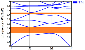
Figure 1. PBG of the TM mode of the structure
Then, by employing the PWE method, the photonic band gap (PBG) of this structure was calculated and obtained as in Figure 1.
Figure 1 illustrates the three regions of PBG for TM mode (see orange region). The first range of “λ” wavelength PBGTM extends from 1448.5 nm to 2155.7 nm, the next TM PBG with wavelength "λ" extends from 825.82 nm to 863.95 nm and for the last PBG of the TM mode its wavelength "λ" goes from 688.32 nm up to 693.68 nm. These ranges are large, medium and narrow respectively and demonstrate that proposed design is suitable for optical communications applications. Then, we have fixed the dielectric constant "a" at 623 nm, knowing that the study will be on a wavelength interval which goes from 1448.5 nm up to 2155.7 nm in TM mode.
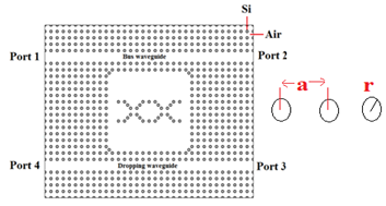
Figure 2. The proposed initial structure
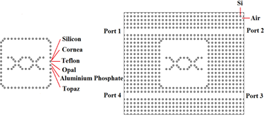
The proposed initial structure of sensor is shown in Figure 2. The design consists of two waveguides in Γ-X direction and single photonic crystal ring resonator sandwiched between them. The core form of the resonant is an ADN –shaped design. The higher waveguide is known as bus waveguide while the lower waveguide is called dropping waveguide. The structure has four ports; the first one is: the input port (1) on the left side of the top (bus) waveguide. The second is: the forward transmission terminal on the opposite side of the waveguide which marked as port (2). The third is the backward drop marked as port (3), and the last one is the forward drop marked as port (4). Optical waves enter the structure through port (1) and then exit to port (2). Nevertheless, at the desired wavelength, the optical wavelengths drop to drop waveguide through the resonant ring and travel toward port (4). The graphic diagram of the sensor is shown in Figure 2.
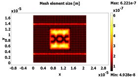
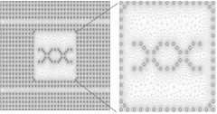
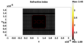
The method of finite element (F.E.M) [23] was used for investigating optical proprieties of the photonic crystals. Obtaining our results from FEM simulations requires 283787 of degrees of freedom, 71158 numbers of mesh points and 141472 triangular number of elements. Therefore, we choose element growth rate to 1.55, mesh curvature factor to 0.65 and mesh curvature cutoff equal to 10-2. The mesh element size and the mesh for all structure are presented in Figure 3a and Figure 3b, respectively. A Figure 3d will give a general overview of the distribution of the refractive index “n” of the dielectric of the pillars along the proposed design. Figure 4d shows the boundary conditions used to obtain the results. The walls of the structure are equipped with the perfect electrical conductor (Ez=0) and the middle in which there are the pillars are put to the conditions of continuity according to the following equation:
$\text{n}\times \left( {{\text{H}}_{1}}-{{\text{H}}_{2}} \right)=0$ (21)
a)
b)
c)
d)
Figure 3. a) The mesh element size, b) the mesh, c) the refractive index and d) the boundary conditions of the proposed structure
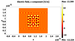
Figure 4. Distribution of an electric field of the initial structure at resonance, λ =1539.945 nm
Knowing that for the input propagation the diffusion boundary conditions including the electric field have been used (E0z=1 V/m,) under the order of the following equation:
$n\times \left( \nabla \times {{\text{E}}_{z}} \right)-j\text{k}{{\text{E}}_{z}}=-j\text{k}(1-\text{k}.\text{n}){{\text{E}}_{0z}}{{\exp }^{jk.r}}$ (22)
With $\mathrm{k}=2 \pi / \lambda$ and for the transmission we used four ports for an input power equal to 1 W and whose equation for the input is:
$S=\int(E-E 1) \cdot E 1 / \int E 1 . E 1$ (23)
And for the rest is of the following form:
With i=2,3 and 4 $S=\int E . E i /E Ei.Ei$ (24)
Next, Figure 4 shows the distribution of an electric field at the resonance inside the proposed structure before the injection of different materials into the resonator. We find the resonance wavelength (λ) for this equal 1539.945 nm.
Figure 5 represents the sensor after injecting the five proposed materials and studying them case by case. The proposed sensor overall size is ≈ 356µm2.
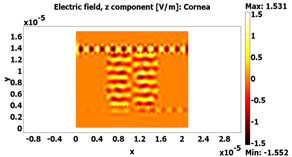
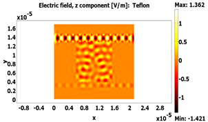
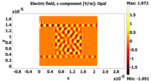
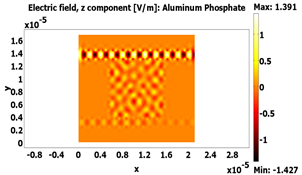
So, Figure 6a, Figure 6b, Figure 6c, Figure 6d, Figure 6w and Figure 6f show the electric field distribution after injection different materials such as, (a) Silicon, (b) human cornea, (c) Teflon, (d) Opal, (e) Aluminum phosphate, and Topaz (f) at resonance wavelength, λ=1.55 µm and which carry the following refractive index: 3.46, 1.3375, 1.36, 1.45, 1.53 and 1.606 respectively.
Figure 5. The proposed sensor
(a) Silicon
(b) Human cornea
(c) Teflon
(d) Opal
(e) Aluminum phosphate
(f) Topaz
Figure 6. Distribution of an electric field of the sensor after injection different materials such as, (a) Silicon, (b) human cornea, (c) Teflon, (d) Opal, (e) Aluminum phosphate, and Topaz (f) at resonance wavelength, λ=1.55 µm
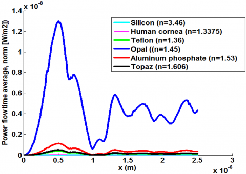
In addition, Figure 7 shows the distribution of the power flow norm as a function of the cross-section line (x) for the different materials proposed for this study at the resonance wavelength, λ=1.55µm from port (1) to port (2), in passing across the resonator to port 3 and port 4.
In general, The Poynting vector is given by [23],
$\bar{P}=\bar{E} \times \bar{H}$ (25)
where, E is electric field; B is magnetic field.
The Eq. (5) represents the power flow per unit area.
Figure 7. The power flow norm of: Silicon (Si), Human cornea, Teflon (C2F4), Opal (SiO2-nH2O), Aluminum phosphate (AlPO4) and Topaz (Al2SiO4 (F; OH)2) versus cross section line (x)
The electromagnetic wave is associated by the density of energy and the latter moves at the speed of the wave. While the total energy density "U" is the addition of the magnetic (UB) and electrical (UE) energy densities [24].
The total energy density equation is given by:
$\mathrm{U}=\mathrm{U}_{\mathrm{E}}+\mathrm{U}_{\mathrm{B}}$ (26)
We have:
$U_{E}=\frac{\varepsilon E^{2}}{2}$ and $U_{B}=\frac{B^{2}}{2} * \mu$
where, “E” is electric field and “B” is magnetic field. And, “ε” is permittivity and “μ” is magnetic permeability.
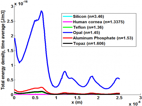
Figure 8. The total energy density of: Silicon (Si), Human cornea, Teflon (C2F4), Opal (SiO2-nH2O), Aluminum phosphate (AlPO4) and Topaz (Al2SiO4 (F; OH)2) versus cross section line (x)
Figure 8 presents the variation of the total energy density (TED) as a function of the cross section line (x) in the structure in its initial state (with silicon pillars) and when the resonator has been replaced by the materials proposed at the resonance.
Thanks to the finite element method (FEM) based on the COMSOL software; we have been able to obtain the numerical results. First, we studied a novel two-dimensional design based on silicon photonic crystals (Si). This design features two waveguides with a resonator in the middle. Knowing that the radius “r” of the pillars is the identical in all design and is worth 118.37 nm and the lattice constant 'a' is 623 nm.
As depicted above, Figure 3a, 3b, 3c and 3d represent the mesh element size, the mesh, the refractive index “n” and the boundary conditions of our design, respectively as well as, Figure 4 as well shows, the distribution of the electric field of the initial design at resonance, λ =1539.945 nm.
The next step aims at investigating the distribution of the electric field of our sensor by replacing five choose materials in the resonator in the structure. Its materials are: Silicon (Si) Human cornea, Teflon (C2F4), Opal (SiO2-nH2O), Aluminum phosphate (AlPO4) and Topaz (Al2SiO4 (F; OH)2) which have the following refractive indices: 1.3375, 1.36, 1.45, 1.53 and 1.606 respectively in versus of the resonance wavelength (m), λ =1.55 µm as shown in Figure 6a, Figure 6b, Figure 6c, Figure 6d, Figure 6e and Figure 6f, respectively.
In addition, Figure 7 presents a clear overview on the standard of power flow (PFN) between port (1) and port (4) through the resonator for the diverse materials previously used. Also, it recapitulates the results of Figure 6, which compares the behavioral degree of the power flow standard (PFN) of the biosensor as a function of the cross section line (x).
Figure 7 shows that the opal (SiO2-nH2O) with a refractive index n = 1.45 reach its maximum power flow norm at 12.97 nW/m2 (with blue curve), followed by aluminum phosphate (AlPO4) (with red curve) and Topaz (Al2SiO4 (F; OH)2) (with black curve) which have a refractive index of 1.53, 1.606 with maximum values of 1.137 nW/m2 and 0.5111 nW/m2 respectively.
Then, the Teflon (C2F4) (with black curve), this material of “n” equal to 1.36, is manifested with a maximum power norm below and not far from that of the topaz which is equal to 0.4167 nW/m2. In addition, a low power of 44.93 pW/m2 is observed in the human cornea (with magenta curve) which has a refractive index of 1.3375. Eventually, we also presented on the same figure and before replacing the materials in the resonator, the normal power of the initial index of refraction of silicon (Si) (with cyan curve) which is equal 3.46 for maximum of power of equal to 5.395 pW/m2. So, the PFN (power flow norm) before the use of the materials is nearly nonexistent. Then, this change in maximum power flow with the possibility of reaching different peaks along the path from port 1 to port 4 is that in the company of the materials used and that its peaks coincide on the same cross section line which is 0.5025 µm.
Figure 8 shows a profile almost similar to that of Figure 7. This figure describes the different states of T.E.D (total energy density) maximum which take the following values: 1.187 * 10-19J/m3, 9.896 * 10-19J/m3, 91.48 * 1019J/m3, 123 * 10-19J / m3, 249.3 * 10-19J/m3 and 2849 * 10-19J/m3, for silicon (Si), human cornea, Teflon (C2F4), topaz (Al2SiO4 (F; OH) 2), aluminum phosphate (AlPO4) and opal (SiO2-nH2O) respectively. Its energy states are displayed as a function of the transverse line according to x. The same behavior of the materials used can be observed as for the power of the norm.
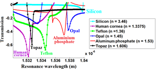
Figure 9. Transmission for silicon (Si), Human cornea, Teflon (C2F4), Opal (SiO2-nH2O), Aluminum phosphate (AlPO4) and Topaz (Al2SiO4 (F; OH)2) versus resonance wavelength
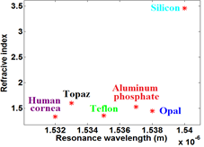
Figure 10. The refractive index of Silicon (Si), Human cornea, Teflon (C2F4), Opal (SiO2-nH2O), Aluminum phosphate (AlPO4) and Topaz (Al2SiO4 (F; OH)2) versus the resonance wavelength (m)
The results obtained from the transmission in dB as a function of the wavelength are presented in Figure 9. From this figure it can clearly be seen that for each material used in this study, the coefficient of transmission reaches peaks of maximums.
In that instance of Opal (SiO2-nH2O), it is obviously that the coefficient of transmission stretches the maximum value which is -0.3834 dB for a wavelength λ = 1.538 μm and for aluminum phosphate (AlPO4), it is -0.455 dB at a wavelength of 1.537 μm and then, for the case of topaz (Al2SiO4 (F; OH)2), the coefficient of transmission stretches a value of -0.596 dB at the wavelength λ = 1.533 μm. In addition, for the last two materials, the Teflon transmission coefficient (C2F4) completes the value of -0.6767 dB at λ=1.535 μm and the transmission coefficient of the human cornea is -0.7758 dB at the wavelength is equal to 1.532 μm.
Figure 10 shows the distribution of the different materials detected by the proposed structure according to their refractive index and their resonant wavelengths. It is found in the initial state where the silicon resonator (n=3.46) is positioned at a resonance wavelength equal to 1.54 μm. As soon as we begin to replace the resonator with the different materials, we observe the change in the level of resonance wavelength over a range of 1.53 to 1.54 microns. This change comes from the index "n" which corresponds to each material. The results of Figure 10 are summarized in Table 1.
Table 1. The resonance of the sensor for six materials (with different indices of refraction)
|
Material |
Human cornea |
Topaz |
Teflon |
Aluminum Phosphate |
Opal |
Silicon |
|
Refractive index (n) |
1.3375 |
1.606 |
1.36 |
1.53 |
1.45 |
3.46 |
|
Resonance wavelength (µm) |
1.532 |
1.533 |
1.535 |
1.537 |
1.538 |
1.54 |
The interest of this work is based on the proposal of a new sensor based on photonic crystals in order to detect some materials, such as human cornea, Teflon, Opal, Aluminum phosphate and Topaz. This sensor consists of a structure made up of two waveguides which traps a resonator between them and convey the signal. This design is achieved through the square array of rods based on two-dimensional photonic crystals that are bathed in the air. The wavelength study interval λ in which this sensor operates is between 1448.5 nm and 2155.7 nm and its area of which is 356.3024 pm2.
The numerical results obtained from the PFN (power flow norm), the TED (total energy density) as well as the transmission obtained by the element method finite, allowed us to observe the different behaviors of the signal in front of the materials used and which is a function of their refractive index “n”. The refractive index is a crucial detection parameter for sensors and this because of its direct influence on the resonant wavelength of each material. The novel sensor proposed in this study is an idea to build a universal sensor that can detect a considerable number of materials at a nanoscale and that can touch several areas including, medical, environmental applications etc.
The present work was supported by the Ministry of Higher Education and Scientific Research of Algeria.
[1] Robinson, S., Dhanlaksmi, N. (2017). Photonic crystal based biosensor for the detection of glucose concentration in urine. Photonic Sensors, 7(1): 11-19. https://doi.org/10.1007/s13320-016-0347-3
[2] Ghoumazi, M., Hocini, A. (2021). Photonic crystal based bio-sensor detection in nanophotonic structure using FEM method. International Journal of Sensors Wireless Communications and Control, 11(2): 216-224. https://doi.org/10.2174/2210327910666191218125109
[3] Olyaee, S., Mohebzadeh-Bahabady, A. (2015). Designing a novel photonic crystal nano-ring resonator for biosensor application. Optical and Quantum Electronics, 47(7): 1881-1888. https://doi.org/10.1007/s11082-014-0053-6
[4] Ghoumazi, M., Hocini, A., Hameurlain, M. (2018). Study and simulation of the power flow distribution of an optical channel drop filter in structure based on photonic crystal ring resonator for different organic liquids. In International Conference in Artificial Intelligence in Renewable Energetic Systems, pp. 544-551. https://doi.org/10.1007/978-3-030-04789-4_58
[5] Chiappini, A., Tran, L.T.N., Trejo-García, P.M., Zur, L., Lukowiak, A., Ferrari, M., Righini, G.C. (2020). Photonic crystal stimuli-responsive chromatic sensors: A short review. Micromachines, 11(3): 290. https://doi.org/10.3390/mi11030290
[6] Ghoumazi, M., Hameurlain, M. (2021). Study and simulation of a sensor based on 2D photonic crystals for the detection of aromatic compounds: C6H5I, C6H5F and C6H5Cl. In Annales de Chimie-Science des Matériaux, 45(4): 335-339. https://doi.org/10.18280/acsm.450409
[7] Mehdi, G., Hocini, A., Hameurlain, M., Boudaa, M. (2018). Novel design of optical sensor based on two-dimensional photonic crystals for the detection of volatile organic compounds that can infect human health. Medical Technologies Journal, 2(4): 293-300. https://doi.org/10.26415/2572-004X-vol2iss4p293-300
[8] Mahmoud, M.Y., Bassou, G., Taalbi, A., Chekroun, Z.M. (2012). Optical channel drop filters based on photonic crystal ring resonators. Optics Communications, 285(3): 368-372. https://doi.org/10.1016/j.optcom.2011.09.068.
[9] Mehdi, G., Hocini, A. (2019). Design of bio-alcohol sensor based on two-dimensional photonic crystal in a nanophotonic structure. In 2019 International Conference on Advanced Electrical Engineering (ICAEE), 1-6. https://doi.org/10.1109/ICAEE47123.2019.9015129.
[10] Panda, A., Pukhrambam, P.D. (2021). Investigation of defect based 1D photonic crystal structure for real-time detection of waterborne bacteria. Physica B: Condensed Matter, 607: 412854. https://doi.org/10.1016/j.physb.2021.412854
[11] Rebhi, S., Massoudi, R., Najjar, M. (2021). Concave rectangle photonic crystal ring resonator for ultra-fast all-optical modulation. Journal of Optical Communications, 42(1): 53-58. https://doi.org/10.1515/joc-2018-0049
[12] Mohammadi, S.F., Khorrami-Nejad, M., Hamidirad, M. (2019). Posterior corneal astigmatism: A review article. Clinical Optometry, 11: 85-96. https://doi.org/10.2147/OPTO.S210721
[13] de Ortueta, D., von Rüden, D., Magnago, T., Mosquera, S.A. (2014). Influence of stromal refractive index and hydration on corneal laser refractive surgery. Journal of Cataract & Refractive Surgery, 40(6): 897-904. http://dx.doi.org/10.1016/j.jcrs.2013.07.050
[14] Chandrasekaran, C. (2017). 9 - Rubber lining for nuclear equipment. Anticorrosive Rubber Lining; Plastics Design Library, 67-72. https://doi.org/10.1016/B978-0-323-44371-5.00009-8
[15] García-Gaytán, V., Bojórquez-Quintal, E., Hernández-Mendoza, F., Tiwari, D.K., Corona-Morales, N., Moradi-Shakoorian, Z. (2019). Polymerized silicon (SiO2· nH2O) in equisetum arvense: Potential nanoparticle in crops. Journal of the Chilean Chemical Society, 64(1): 4298-4302. http://dx.doi.org/10.4067/s0717-97072019000104298.
[16] Maurin, I., Moufarej, E., Laliotis, A., Bloch, D. (2015). Optics of an opal modeled with a stratified effective index and the effect of the interface. JOSA B, 32(8): 1761-1772. https://doi.org/10.1364/JOSAB.32.001761
[17] https://fr.wikipedia.org/wiki/Opale.
[18] Mei, C., Deshmukh, S., Cronin, J., Cong, S., Chapman, D., Lazaris, N., Kirkitadze, M. (2019). Aluminum phosphate vaccine adjuvant: analysis of composition and size using off-line and in-line tools. Computational and Structural Biotechnology Journal, 17: 1184-1194. https://doi.org/10.1016/j.csbj.2019.08.003
[19] Kalbfleisch, K., Deshmukh, S., Mei, C., Ore, M., Williams, W., Durowoju, I., Kirkitadze, M. (2019). Identity, structure and compositional analysis of aluminum phosphate adsorbed pediatric quadrivalent and pentavalent vaccines. Computational and Structural Biotechnology Journal, 17: 14-20. https://doi.org/10.1016/j.csbj.2018.11.006
[20] Dumańska-Słowik, M., Toboła, T., Natkaniec-Nowak, L., Pedrosa-Soares, A.C. (2016). Characteristics of inclusions in topaz from Serrinha pegmatite (Medina granite, Minas Gerais State, SE Brazil) studied by Raman spectroscopy. Vibrational Spectroscopy, 85: 196-201. https://doi.org/10.1016/j.vibspec.2016.04.019
[21] Trujillo-Vázquez, E., Pech-Canul, M.I., Marcazzó, J. (2016). Thermoluminescent characterization of Al2O3-derived synthetic topaz. Journal of Alloys and Compounds, 689: 500-506. http://dx.doi.org/10.1016/j.jallcom.2016.08.014
[22] Vijaya Shanthi, K., Robinson, S. (2014). Two-dimensional photonic crystal based sensor for pressure sensing. Photonic Sensors, 4(3): 248-253. https://doi.org/10.1007/s13320-014-0198-8
[23] Rahman, B.M.A., Leung, D.M.H., Kejalakshmy, N., Agrawal, A., Grattan, K.T.V. (2012). Finite element solutions of nanophotonics devices. In AIP Conference Proceedings, 1504(1): 1283-1286. https://doi.org/10.1063/1.4772164
[24] Saslow, W.M. (2002). Electricity, Magnetism, and Light. Maxwell's Equations and Electromagnetic Radiation. Chapter 15: 630-677. https://doi.org/10.1016/B978-0-12-619455-5.X5000-1