Fadila Souad Nouar* | Mimouna Oukli | Mohamed Khadraoui
© 2021 IIETA. This article is published by IIETA and is licensed under the CC BY 4.0 license (http://creativecommons.org/licenses/by/4.0/).
OPEN ACCESS
The aim of this work is to simulate correctly in 3D space the phenomena that govern relaxation semiconductors. To avoid the relevant constraints of inadequate mesh a new technique for refining irregular meshing has been creating. Each length of the sample will be considered as a partial sum of a geometric series, the calculation of the argument of this series, will allow to calculate the distance between the nodes. In this paper we proposed to use an algorithm combined between Gummel and Newton Raphson algorithms to solve the partial differential equations, the linearization of transport equations is obtained by applying the finite difference method, which allowed us to calculate the relaxation time, life time and recombination rate. The results revealed appearance of a limited region called recombination front instead of charge space region, an improvement in computational time with a big precision for a 3D simulation, by letting to the user the choice of the distance to be discreet and the number of points wished without saturate the memory. This type of meshing is simple to apply and can be used to be applied as a solution to correctly simulate phenomena in structures at different areas for all the dimensions.
finite difference method, Gummel’s algorithm, Newton’s algorithm, geometric series transport equations, recombination rate, relaxation time, lifetime
The three-dimensional simulation of devices is very important [1]. Calculations are extremely accurate and can take into account many parameters for a very thorough study. The presence of critical areas in the latter’s with small dimensions compared to the general structure, requires us to either exploit all the nodes in these regions without correctly simulating the general structure, either to simulate the whole device with coarse mesh and neglect the critical regions and distort the correct description of phenomena.
Currently, three-dimensional simulation of complex geometry devices involves long computational times at very high costs, given the importance of the nodes used to properly represent these structures. In many cases, when an inadequate mesh is applied, entire surfaces disappear, in addition to memory saturation and a very long simulation time. Several studies propose irregular meshing, without giving the user the choice to increase the number of desired points in certain areas, where the theoretical study approves the existence of important phenomena in these regions.
To resolve these defects, this paper establishes a model based on a simple new technique of refining irregular mesh, with the aim of concentrating maximum points in critical regions and less in less important regions, we placed the initial point at the beginning of the critical zone, and the rest of the points over a distance that progresses in geometric series, this allows to calculate the desired parameters at the level of all the nodes of the structure with better convergence, and therefore a considerable improvement in computational time.
To apply this method one will propose to simulate a relaxation semiconductor [2, 3] where the Finite-Difference method [4] which has gained considerable popularity over the past two decades, and which is often the method of choice for material distributions was chosen to calculate the potential, concentration of free transporters, relaxation time, lifetime and recombination rate, The resolution method consists of the linearization of transport equations [5] by the finite difference method [6, 7], the algorithm most suited to the resolution of heavily coupled nonlinear equations [8, 9] is that of Newton-Raphson.
The paper is structured as follows: The Three-Dimensional Representation of Physical Equations briefly described in Section 2. The test structure is described and presented in Section 3. The numerical model established is proposed in Section 4. The most relevant results obtained are presented and discussed in Section 5. Finally, in Section 6 we summarize the main conclusions of this work.
For the analysis of a homogeneous three-dimensional structure in the stationary case, and to be able to calculate the concentration of free carriers and potential, it is essential to solve the basic Poisson's and continuity equations take the form above.
$\left\{\begin{array}{l}f_{\psi}=\frac{\partial^{2} \psi}{\partial x^{2}}+\frac{\partial^{2} \psi}{\partial y^{2}}+\frac{\partial^{2} \psi}{\partial z^{2}}-\frac{q}{\varepsilon} \\ \left(n-p+N_{D}^{+}-N_{A}^{-}-n_{r}\right)=0 \\ f_{n}=\frac{1}{q} \cdot\left(\frac{\partial j_{n}}{\partial x}+\frac{\partial j_{n}}{\partial y}+\frac{\partial j_{n}}{\partial z}\right)-U_{n}=0 \\ f_{p}=\frac{1}{q} \cdot\left(\frac{\partial j_{p}}{\partial x}+\frac{\partial j_{p}}{\partial y}+\frac{\partial j_{p}}{\partial z}\right)+U_{p}=0\end{array}\right.$ (1)
where, jn and jp are Vector current densities of electrons and holes, n is electrons densities, ND+ and NA- are Donors and acceptors ionized densities, nr is the charge trapped on a deep center, p is Free holes densities, $\psi$ is electrostatic potential, q is the elementary charge of the electron and U is the recombination rate.
Two characteristic times allow defining both categories of semiconductors:
(1) Lifetime semi-conductor where for a lifetime value τ0 very upper in the time of dielectric relaxation τrd (τrd <<τ0)
(2) Relaxation semiconductor Should the opposite occur or τ0 is very lower in the time of Dielectric relaxation τrd (τrd>>τ0)
In the case of lifetime semiconductors, the obtained results can be analyzed by using of simple injection and by supposing a common lifetime of the carriers in excess wich is constant for electrons and holes through the region ν this type of semiconductor will be called a life semiconductor according to Van Roosbroeck’s terminology.
Should the opposite occur in the case of relaxation semiconductors, the effects of load of space is very important by everything and the life expectancies of the carriers in excess vary a great deal of a point to another one along the structure. This type of semiconductor will be called relaxation semiconductor. It is the case of GaAs.
After solving of the Eq. (1) we can calculate, the relaxation time τrd and the lifetime τ0 according to Eqns. (2) and (3):
$\tau_{r d=} \frac{\varepsilon}{e\left(n_{e} \mu_{n}+p_{e} \mu_{p}\right)}$ (2)
$\tau_{o=} \frac{\tau_{n e}\left(p_{e}+p_{t}\right)+\tau_{p e}\left(n_{e}+n_{t}\right)}{\left(n_{e}+p_{e}\right)}$ (3)
where, e is the electron electrical charge, $\mu_{n}$ and $\mu_{p}$ are Mobility of electrons and holes, ne is the electrons densities at equilibrium thermodynamic, pe is the Free holes densities at equilibrium thermodynamic.
The dielectric permittivity of semiconductor is defined in Eq. (4) as:
$\varepsilon=\varepsilon_{o} . \varepsilon_{r}$ (4)
where, $\varepsilon_{o}$ is the permittivity of vacuum, $\varepsilon_{r}$ is the Relative permittivity of semiconductor.
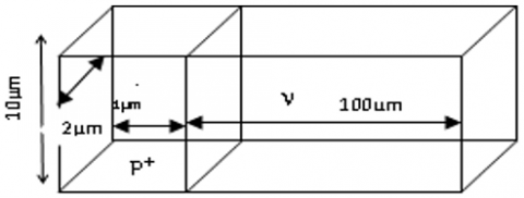
The studied structure, is a structure pν [10, 11], given by Figure 1, where the layer ν is slightly N-type. We handle the case of relaxation semi-conductors and we suppose that the conditions in the limits are the ones of the balance thermodynamics, and we are going to use two types of conditions in the limits that of Dirichlet and Neumann. The resolution of the Eq. (1) is made in three dimensions.
Figure 1. Structure used in the test
All the numerical values of the electric and geometrical parameters relative to the structure of the test [11] are given in Table 1:
Table 1. Physical and geometrical parameters of the structure
|
Regions |
Physical parameters |
Geometrical parameters (Thickness) |
|
Structure Pν |
KT=26 .10-3 ev $\mathcal{E}_{r}$=11 $\mu_{n}$=4000 cm2/v $\mu_{p}$=280 cm2/v.s ni=3.108 cm-3 |
Wp=101 µm |
|
Zone P |
NA=2.1016 cm-3 |
Wp=1 µm |
|
Zone ν |
ND=1.5.1011cm-3 n1=3.109cm-3 p1=3.107cm-3 $\tau_{n t}$=$\tau_{p t}$=10-11 s |
Wp=100 µm |
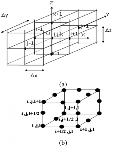
The Finite-Difference method [12] is now applied to solve the whole Eq. (1), to solve this problem, and by applying our method of meshing we have discretized the region of interest in a large number of elements, the calculation of physical quantities is determined to any point of discretization in all the directions X, Y and Z. The node of the meshing is presented in Figure 2a. The geometry is given in an element of Hexaidric, as comic to the Figure 2b.
Figure 2. Geometric representations with a Hexaidric element
In relaxation semiconductor the effects of load of space are very important by everything and the life expectancies of the carriers in excess vary a great deal of a point to another one along the structure.
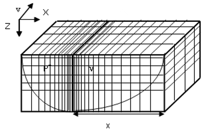
A regular mesh may neglect certain areas where the variation in lifetime and relaxation time is important throughout the entire structure, an irregular mesh is required to take maximum points in the critical areas, without ignoring the other areas, The chosen model is a junction PN where the phenomena of transport are concentrated in the space charge region. A precise meshing has to take into account for complement the study in the most important domains. Our method of calculation based on the geometrical series, allows to create an irregular mesh. The latter can be unrefined in regions neutral and refined in the nearby regions of interface of P+ as shown in Figure 3.
Figure 3. Presentation of progressive irregular meshing
The length of the whole area will be considered the sum of a geometric series, whose initial step will be fixed and its reason is calculated, allowing the calculation of successive discrete distances that will progress through a geometry series more and more that we move away from the critical zone according to Eq. (5):
$x_{i+1}=x_{i} * r$ (5)
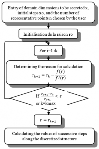
After choosing the distance to discretize x, it is necessary to choose the initial point x0 and the number of points wished on this distance, by being careful not to exceed the capacity maximal memory of our machine. When the geometrical and physical parameters are introduced, the procedure of meshing presented in Figure 4.
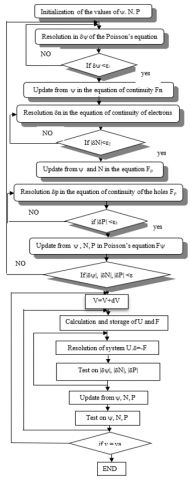
The study of the relaxation semiconductor in the presence of one or several deep centers pull the complexity in the description of the phenomena of transport [13]. Where from a difficulty of implementation of a program which holds in account this phenomenon. The decrease of the life time causes a hyperbolic relation between the densities of electrons and holes, what makes difficult the application of the method decoupled by Gummel [14, 15]. However, its use in equilibrium thermodynamics remains an essential stage, where the results will be injected as values initial in the method of Newton [16, 17] who is the most suited for the study of these components under polarization, to allow better one convergence and consequently an improvement in the tridimensional calculation often prohibitive, a combined method, integrating at the same time the algorithm of Newton and that of Gummel was finalized, presented in Figure 5.
This method is combined enter methods Gummel and that of the Newton, by applying a non-uniform meshing reserving a maximum of points in the zones of loads of space and less clear in the neutral zones, so allowing to win a considerable time of execution for the three-dimensional calculations.
Figure 4. Discretization and determination of calculating steps
Figure 5. Algorithm of the combined method
5.1 Impact of meshing
We used in this simulation the software DEV C++ version 5 [18, 19]. This version gives the possibility to declare three-dimensional arrays with a maximum size of 150*150*150. We chose to take a minimum of points (15) in P + region and 135 points in the N region, which can be physically argued because the space load region extends essentially in the less doped region N.
The simulations were realized on a microcomputer with the microprocessor Intel3 for 2460375 nodes (135 * 135 * 135) by the use of a method combined between the algorithm of Gummel and that of the Newton.
Although the equations are strongly coupled integrating a strong density of the traps included in the Poisson’s equation (NT=2.1016cm-3), we were able to approximal the results with a satisfactory precision of the order of 10-4 in a calculation time of 61 hours 32 minutes in a three-dimensional space.
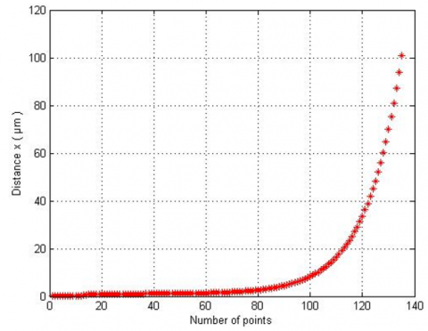
Our meshing offers the possibility of having more points in the critical domains where the accuracy of the results is important and a minimum of points in the neutral regions is illustrated in Figure 6.
Figure 6. Discretization points calculated by geometric series
Figure 7. Representation of the discretization points on a logarithmic scale calculated by geometric series
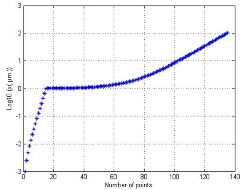
To observe better this meshing, we traced the distance on a logarithmic scale in Figure 7.
In the figure above traced by MATLAB [20], we notice a better representation of the critical zones and a condensation of a very high number of points in the of load space region, which begins to decrease more and more when we go away from this zone.
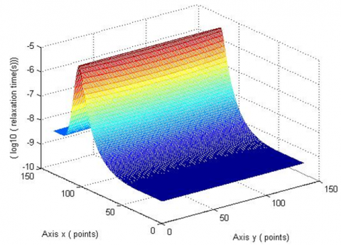
The calculation of the potential, the concentration of electrons and free holes in the balance thermodynamics [10], gives us the possibility of calculating the same parameters under a polarization of 10 KT/q [10], where from we can calculate the relaxation time and the life time for the structure in Eqns. (3) and (4) represented respectively in Figures 8 and 9.
Figure 8. Relaxation time τrd
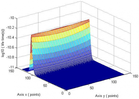
Figure 9. Life time τ0
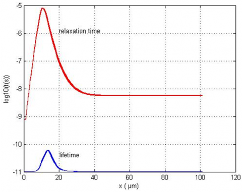
In these last figures, we notice clearly the impact of our meshing on the studied geometry, a very good distribution of points and a very good representation of the critical zones which is closer to the region P+ was observed. To understand the phenomena, which govern, we are going to redraw the graphs of the times of relaxation and life expectancy according to the real distance, presented in the following figure:
Figure 10 shows that the relaxation time is much bigger than the life time throughout the structure, what proves that we are in the presence of a relaxation semiconductor (τrd > τ0).
The application of our meshing allowed us to notice that two calculated times are not constant during the structure so we were able to model correctly all the parts of structure in a precise way, contrary to other meshing’s regular which allow to model objects, where whole surfaces disappear.
Figure 10. Comparison between relaxation and life time
5.2 Physical interpretation
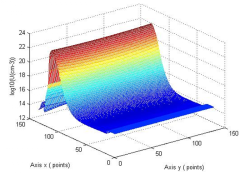
For the interpretation of the phenomena, which govern in the relaxation semiconductor, we go tracer the distribution of the rate of recombination U given by the Eq. (5) as shown in Figure 11. Shockley Read takes into account all the processes of recombination generation of thermal origin on a center situated in the forbidden band:
$U=\frac{n p-n_{i}^{2}}{\tau_{p}\left(n+n_{1}\right)+\tau_{n}\left(p+p_{1}\right)}$ (6)
where, niis the intrinsic concentration.
In this case, the recombination does not occur uniformly through the space charge region, but in a limited zone called recombination front the length of which is of the order of 10 µm confirmed in Figure 11.
Figure 11. Rate recombination for a voltage at 10 KT/q
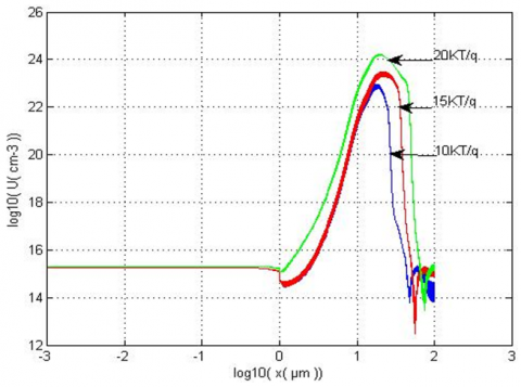
To better notice the influence of the polarization on the rate of recombination we go traced the evolution of the rate of recombination function of the polarization in Figure 12.
Since one is in the presence of a relaxation semi-conductor where τrd > τ0, and to maintain the electric neutrality, the semiconductor returns to its electric neutrality before having time to recombine, what explains the decrease of the concentration of free electrons, and consequently the increase of the rate of recombination in the part of the recombination front.
The values of n and P in the neutral zones keep the same values at thermodynamic equilibrium [8]. But, except balance and under direct polarization, a decrease of the barrier of tension was observed, what favorites the passage of the holes from Part P to part ν Who is translated by the increase of the variation in the occupancy of the booby-trapped center Δpt, and who explains the increase of the density of the concentration of holes.
Figure 12. Rate recombination for different polarization voltage
The three-dimensional simulation method with an irregular mesh progressing in geometric series using the linearization of transport equations by the finite difference method presents the peculiarity, to distribute an important set of nodes in critical regions and the rest of points in regions less important, without requiring the construction of a regular meshing which uses a significant number of points without concentrating on the interesting zones, with costs of very important additional calculations.
The example treated of relaxation semiconductors using this type of meshing where The not linear equations with the partial differences ensuing from the physical model are discretizes by the finite difference method and resolved by the use of Gummel’s and Newton’s algorithms, revealed fronts of recombination instead of charge space region by the calculation of relaxation time, life time and the rate of recombination of a junction P+N, with a big precision in a short time for a three-dimensional simulation , By letting to the user the choice of the distance to be discreet and the number of points wished without for it to saturate the memory, this type of meshing is simple to apply and can be to use for all the structures and for all the dimensions.
As perspective for this work is to applying this meshing on devices where the complex geometric effect has an impact on physical and electrical values, more that we can use version of the software with a parallel development executed on a process network to reduce even more the computational time resulting from three-dimensional simulations.
|
Dn |
Diffusion of electrons constants |
|
Dp |
Diffusion of holes constants |
|
e |
The elementary charge of the electron=1.6.10-19 C |
|
jn |
Vector current densities of electrons A/cm2 |
|
jp |
Vector current densities of holes A/cm2 |
|
n |
Electrons densities, cm-3 |
|
NA |
Acceptors ionized densities, cm-3 |
|
ND+ |
Donors ionized densities, cm-3 |
|
ne |
Free Electrons densities at equilibrium thermodynamic, cm-3 |
|
ni |
Intrinsic concentration, cm-3 |
|
nt |
The charge trapped on a deep center, cm-3 |
|
p |
Free holes densities, cm-3 |
|
pe |
Free holes densities at equilibrium thermodynamic, cm-3 |
|
U |
Rate of recombination, cm-3 |
|
Greek symbols |
|
|
$\mathcal{E}$ |
The dielectric permittivity of the semiconductor |
|
$\mathcal{E}_{o}$ |
The permittivity of vacuum=8.854.10-12 F/m |
|
$\mathcal{E}_{r}$ |
The Relative permittivity of the semiconductor |
|
$\psi$ |
Electrostatic potential, v |
|
$\mu_{n}$ |
Mobility of electrons, cm2/v |
|
$\mu_{p}$ |
Mobility of and holes, cm2/v |
|
σn |
Electrical conductivity of the electrons, S.m-1 |
|
σp |
Electrical conductivity of the holes, S.m-1 |
|
τ |
Time of mean free path, s |
[1] Shamsir, S., Hasan, M.S., Hassan, O., Paul, P.S., Hossain, M.R., Islam, S.K. (2020). Semiconductor device modeling and simulation for electronic circuit design. Modeling and Simulation in Engineering - Selected Problems. https://doi.org/10.5772/intechopen.92037
[2] Ngo, C., Ngo, H. (2003). Les semi-conducteurs de l'électron aux dispositifs edition Dunod.
[3] Jones, B.K., Sengouga, N., Dehimi, L. (2000). Relaxation semiconductor diodes: A practical review. In 2000 International Semiconductor Conference. 23rd Edition. CAS 2000 Proceedings (Cat. No. 00TH8486), Sinaia, Romania, pp. 323-326. https://doi.org/10.1109/SMICND.2000.890246
[4] Çapoğlu, I.R., Taflove, A., Backman, V. (2013). Angora: A free software package for finite-difference time-domain electromagnetic simulation. IEEE Antennas and Propagation Magazine, 55(4): 80-93. https://doi.org/10.1109/MAP.2013.6645144
[5] Mathieu, H. (2009). Physique des semi-conducteurs et des composants électroniques Cours et exercices corrigés.6th edition Masson, Paris.
[6] Schneider, J.B. (2010). Understanding the FDTD Method. School of Electrical Engineering and Computer Science, Washington State University.
[7] Taflove, A. (2005). Computational Electrodynamics: The Finite-Difference Time-Domain Method. Artech House.
[8] Jedrzejeiwski, F. (2010). Introduction Aux Méthodes Numériques. 2 Edition. Springer.
[9] Grivet, J.P. (2013). Méthodes Numériques Appliquées pour le Scientifique et L’Ingénieur (Grenoble Science). EDP Sciences.
[10] Souad, N.F., Seddik, M., Mohamed, A., Pierre, M., Ahmed, M. (2015). Three-dimensional devices transport simulation lifetime and relaxation semiconductor. International Journal of Electrical and Computer Engineering, 5(2): 243-250.
[11] Ardebili, R. (1992). Etude par simulation numérique du transport dans las semiconducteurs en présence des centres profonds. Thesis PhD, Centre Montpellier Electronics.
[12] Choudhari, A.V., Pande, N.A., Gupta, M.R. (2013). Feasibility analysis of low-cost graphical processing units for electromagnetic field simulations by finite difference time domain method. International Journal of Computer Applications, 67(24): 30-33. https://doi.org/10.5120/11739-7396
[13] Manifacier, J.C. (2008). Theoretical and numerical investigations of carrier’s transport in N-semi-insulating-N and P-semi-insulating-P diodes - A new approach. Solid-State Electronics, 52(8): 1162-1169. https://doi.org/10.1016/j.sse.2008.04.029
[14] Corriou, J.P. (2010). Méthodes numériques et optimisation Théorie et pratique pour l’iingénieur. Éditions Paris TEC et doc.
[15] Chen, R.C., Liu, J.L. (2003). Monotone iterative methods for the adaptive finite element solution of semiconductor equations. Journal of Computational and Applied Mathematics, 159(2): 341-364. https://doi.org/10.1016/S0377-0427(03)00538-7
[16] Sakowski, K., Marcinkowski, L., Krukowski, S. (2013). Modification of the Newton’s method for the simulations of gallium nitride semiconductor devices. In International Conference on Parallel Processing and Applied Mathematics, pp. 551-560. https://doi.org/10.1007/978-3-642-55195-6_52
[17] Knapp, E., Häusermann, R., Schwarzenbach, H.U., Ruhstaller, B. (2010) Numerical simulation of charge transport in disordered organic semiconductor devices. Journal of Applied Physics, 108(5): 054504. https://doi.org/10.1063/1.3475505
[18] Delannoy, C. (2017). Programmer en Langage C++. Edition Eyrolles, Paris.
[19] Stroustrup, B. (2012). Principes et pratiques avec C++. Edition Pearson.
[20] Mokhtari, M. (2010). MATLAB R2009, SIMULINK et STAFLOW pour Ingénieurs, Chercheurs et Etudiants. Springer.