Anass Slamti* | Youness Mehdaoui | Driss Chenouni | Zakia Lakhliai
© 2021 IIETA. This article is published by IIETA and is licensed under the CC BY 4.0 license (http://creativecommons.org/licenses/by/4.0/).
OPEN ACCESS
A novel internal compensation technique named dual frequency compensation is proposed to improve the stability and the transient response of the on-chip output capacitor three stage low-drop-out linear voltage regulator (LDO). It exploits a combination of amplification and differentiation to sufficiently separate the dominant pole from the first non-dominant pole so that the latter is located after the unity gain frequency regardless of the load current value. The proposed LDO regulator is analyzed, designed, and simulated in standard 0.18 µm low voltage CMOS technology. The presented LDO regulator delivers a stable voltage of 1.2 V for an input supply voltage range of 1.35-1.85 V with a maximum line deviation of 4.68mV/V and can supply up to 150mA of the load current. The maximum transient variation of the output voltage is 54.5 mV when the load current pulses from 150mA to 0mA during a fall time of 1µs. The proposed LDO regulator has a low figure of merit compared with recent LDO regulators.
power management, system on a chip (SoC), Low-Drop-Out regulator (LDO), stability, minimum load current, transient load regulation, CMOS technology
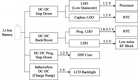
Many system-on-a-chip (SoC) applications integrate circuit blocks, such as digital, analog and radio-frequency blocks [1-4]. Charge pump regulators are commonly used to generate high voltages for lighting or memory units [5, 6]; switching converters are employed to regulate digital blocks, due to their high power efficiency [7, 8]; and low-drop-out linear voltage regulators are used to provide low noise supply voltage with very low ripple for noise sensitive blocks, such as analog/RF circuits [9, 10]. An example that highlights the present-day importance of voltage regulators and power management blocks can be found in ref. [11], where the power supply requirements for a Code-Division Multiple Access (CDMA) modem of a mobile phone are described. As shown in Figure 1, LDO regulators play a very important role in the integrated power management unit in modern portable electronic devices [11], they scales down the supply voltage to provide for many various other blocks.
An important issue in LDO voltage regulator design is stability, which has a direct impact on the transient response of this system. In addition, the downscaling of the supply voltage and the decrease of the intrinsic gain of the MOS transistor for nanometric CMOS technologies [12, 13] requires the use of multiple stages in the implementation of the LDO regulator, this degrades the close-loop response by the presence of multiple poles, hence the need to develop a robust compensation method. Compensation can be external or internal. Generally, external compensation is achieved with a high value capacitor in the order of µF [14]. As for internal compensation, Miller compensation is one of the most widely used techniques [10], but other techniques and approaches can be found in literature [15-28].
Figure 1. Power management unit in modern portable devices [11]
In this work a novel frequency compensation technique is proposed to achieve the stability for wide range of the load current for the LDO regulator and also enhance his transient response. In section 2, a literature review of stability enhancement is summarized. In section 3, the proposed LDO regulator circuit is given and detailed analysis is performed. In section 4, the simulation results are given to show the performance of the proposed LDO regulator in terms of stability, transient response and others parameters accompanied by a comparison with previous related works. Finally, in section 5, the simulation results are given to show the performance of the proposed LDO regulator in terms of stability, transient response and others parameters accompanied by a comparison with previous related works.
Many solutions have been proposed in the literature to improve the stability of LDO regulators with small current load values. One of the earliest proposals [15] uses a compensation block to control the damping factor [16]. This improves the stability of the system and increases the bandwidth. A variant of this work can be found in [17], where a block is introduced to control the quality factor of the pair of non-dominant complex poles. To save power, the active load of the differential pair of the error amplifier is reused as a current buffer. An additional branch is included to introduce a zero in the negative real half-plane with the twofold objective of improving the stability and increasing the maximum current at the gate of pass transistor. Unfortunately, every stage of the control circuit is loaded by compensating capacitors, which causes a decrease in the Slew-Rate (SR) of the LDO regulator. Capacitive multipliers were also used in [18-22]. As an example, in [18], a differentiator, formed by a capacitor and a current buffer, is introduced. This buffer serves a double purpose. First of all, it introduces a fast path between the output of the LDO regulator and the gate of pass transistor. Second, the buffer helps to separate the poles, since the capacitor appears at the gate of pass transistor multiplied by the gain of the current buffer. It is worth noting that the use of a current buffer is compatible with other compensation techniques. As an example, in [22], a current buffer is used as part of a classical Reverse Nested Miller Compensation (RNMC). In [23], adaptive power transistors technique is proposed to allow the LDO regulator to transform itself between two stage and three stage cascaded topologies with respective power transistor, depending on the load current condition. This later technique achieves high stability and good transient response. Most of these techniques and approaches suffer from the instability problem at very low load current, while several applications need the LDO regulator to hold the output and provide good performance under a no-load current condition such as CMOS RAM keep-alive applications.
To overcome the limitations of the classical internal compensation, an alternative topology called Flipped Voltage Follower (FVF) has been proposed [24]. This method has been well analyzed, developed and applied to the LDO regulator [25], it is characterized by a local feedback which makes it possible to achieve a low output impedance, and consequently to improve the SR at the gate of pass transistor, which improves the transient response as well as the stability, but because of the low value of the static gain generated by this method [25], the performance of the line and load regulations remains limited which degrades the transient response. To improve the performance of stability and regulation, several LDO regulators have been proposed, such as the one that uses the Cascode Flipped Voltage Follower [26], the multiple-loop LDO regulator based on the flipped voltage follower [27] and the LDO regulator with mixed internal compensation which marries the Miller compensation and the flipped voltage follower [28].
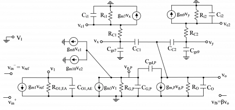
3.1 Main blocks of proposed LDO regulator
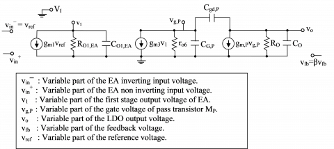
The diagram block of proposed LDO regulator is shown in Figure 2, while Figure 3 gives transistor implementation of proposed error amplifier (EA). For error amplifier design, a single-ended two-stage error amplifier with fully differential input is chosen [29], it consists of M1-M6 transistors, bias current IB,EA and common feedback resistor RCM. A fully-differential PMOS M1 input stage is used to achieve high power supply noise rejection. The third stage is composed by the PMOS pass transistor MP to achieve low dropout voltage [10]. The feedback network is composed by the resistors RFB1 and RFB2. RL is the load resistor which models the low voltage system-on-chip powered by the LDO regulator output. The load capacitor CL is integrated on chip, which is essential to improve the transient response. VI is the power supply input voltage, VREF is the reference voltage provided by another sub-circuit, VG,P represent the voltage at the gate of pass transistor MP. VO is the output voltage of LDO regulator. The compensation network will be clarified later in this section.
Figure 2. Block diagram of the proposed LDO regulator
Figure 3. Proposed error amplifier (EA)
3.2 Stability analysis
3.2.1 Uncompensated frequency response
To determine the uncompensated open-loop transfer function, of the proposed LDO regulator system, defined by Eq. (1), a small signal model is established and it is represented in Figure 4. By applying the Kirchhoff current laws, we obtain the transfer function Hol,u(s) given by Eq. (2). Where, H0,u is the DC gain given by Eq. (3), where β is the feedback factor expressed by Eq. (4). gm1 is the transconductance of the EA first stage which is equal to that of transistor M1 and RO1,EA represents the output resistance of the EA first stage expressed by Eq. (5), where ro1 and ro2 represent the small output resistances of transistors M1 and M2, respectively. gm3 and gm,P represent the transconductance of EA second stage, which is equal to that of transistor M3, and the transconductance of pass transistor MP, respectively. ro6 is the small signal output resistance of EA second stage which is equal to small signal output resistance of transistor M6. RO is the output resistance of LDO regulator given by Eq. (6), where ro,P is the output resistance of MP. Note that s denotes the complex variable of Laplace.
Figure 4. Small signal model of the proposed uncompensated LDO
${{H}_{ol,u}}(s)=\frac{{{v}_{fb}}}{{{v}_{ref}}}$ (1)
${{H}_{ol,u}}(s)=\frac{{{H}_{0,u}}(1+\frac{s}{{{z}_{RHP}}})}{(1-\frac{s}{{{p}_{d}}})(1-\frac{s}{{{p}_{nd}}})(1-\frac{s}{{{p}_{3}}})}$ (2)
${{H}_{0,u}}=-\beta {{g}_{m1}}{{g}_{m3}}{{g}_{m,P}}{{R}_{O1,EA}}\quad{{r}_{o6}}{{R}_{O}}$ (3)
$\beta =\frac{{{R}_{FB2}}}{{{R}_{FB1}}+{{R}_{FB2}}}$ (4)
${{R}_{O1,EA}}={{r}_{o1}}//{{r}_{o2}}//{{R}_{CMFB}}$ (5)
${{R}_{O}}={{r}_{o,P}}//({{R}_{FB1}}+{{R}_{FB2}})//{{R}_{L}}$ (6)
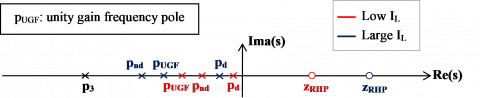
The transfer function contains a right half-plane (RHP) zero zRHP given by Eq. (7), where Cgd,P is the parasitic drain-to-source capacitance. The frequency location of zRHP changes with load current IL (or value of RL), because gm,P and Cgd,P change with IL and this is due to the fact that Mp changes the region of operation according to the variation range of IL [9].
${{z}_{RHP}}=\frac{{{g}_{m,P}}}{{{C}_{gd,P}}}$ (7)
According to Eq. (2), the transfer function contains three left half-plane (LHP) poles pd, pnd and p3, where their locations change relatively with the load current. The dominant pole pd is located at the gate node of MP (vg,P voltage in Figure 4) due to the large value of CG,P and ro6, where CG,P represents the total capacitance connected between the MP gate and the small signal ground. The non-dominant pole pnd is located at the output node (vo voltage in Figure 4). The third pole p3 represents the high frequency pole and it’s located at the first stage output node of EA (v1 voltage in Figure 4). This last pole is independent of the load current and therefore does not affect the stability. For the proposed LDO regulator design, Mp operates in sub-threshold region when the load current is at its minimum value IL,min, while it operates in the saturation region at the maximum value IL,max of load current. In this case the approximate expressions of these three poles are given by:
${{p}_{d}}\approx -\frac{1}{{{r}_{o6}}\quad({{g}_{m,P}}\quad{{R}_{O}}{{C}_{gd,P}}\quad+{{C}_{G,P}}\quad)+{{R}_{O}}{{C}_{O}}}$ (8)
${{p}_{nd}}\approx -\frac{{{r}_{o6}}\quad({{g}_{m,P}}\quad{{R}_{O}}{{C}_{gd,P}}+{{C}_{G,P}})\quad+{{R}_{O}}{{C}_{O}}}{{{R}_{o6}}\quad{{R}_{O}}({{C}_{gd,P}}\quad+{{C}_{G,P}}\quad){{C}_{O}}}$ (9)
${{p}_{3}}\approx -\frac{1}{{{R}_{O1,EA}}\quad{{C}_{O1,EA}}}$ (10)
where, CG,P=CO2,EA+Cgd,P and CO=CL+Cdb,P. CO1,EA and CO2,EA represent the output capacitances of EA first stage and EA second stage, respectively. Cgd,P, Cgs,P and Cdb,P represent the parasitic capacitances gate-to-drain, gate-to-source and drain-to-bulk of the pass transistor MP.
(a) Bode plan location
(b) complex s plan location
Figure 5. Pole-zero location with load current variation
Figure 5 shows the dependence of zeros and poles location on the load current IL in the Bode plan and in the complex s plane, respectively. The frequency location is presented in term of angular frequency ω, where ωzRHP=zRHP, ωpd=−ωpd, ωpnd=−pnd and ω3=−p3. For low IL, the RHP zero is located in the middle frequencies, which introduces a phase shift of −90°, this pushes the non-dominant pole towards the low frequencies, before the unity gain angular frequency ωUGF. Therefore the magnitude curve in the Bode diagram intersects the frequency axis by a slope of −40 dB/decade and consequently the LDO regulator is unstable. For a case of the large load current, the RHP zero is pushed in the high frequencies, the non-dominant pole is located after the unity gain frequency, so the phase margin is positive but insufficient (less than 45°) to stabilize closed loop response of the LDO regulator system.
It is clear that to stabilize the LDO regulator, it is necessary to separate the dominant and non-dominant poles while keeping a phase margin greater than 45 degree for the entire load current range required by the specifications and keeping higher the unity gain frequency to have a fast transient response, this is achieved by adding a LHP zeros well placed with respect to the non-dominant pole and unity gain frequency locations.
3.2.2 Compensated frequency response
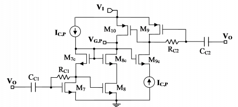
To stabilize the proposed three stage LDO regulator, a dual compensation circuit has been inserted between the LDO output and the pass transistor gate. The compensation network is given by Figure 6. It is composed of two differentiator-current amplifier blocks, (CC1, RC1, M7, M8) and (CC2, RC2, M9, M10), whose role is to separate the dominant pole from the first non-dominant pole and to create LHP zeros to increase the phase margin. The proposed compensation block has no effect on the elimination of the RHP zero. The compensation circuit requires a symmetrical bias current IB,C. The cascode trasistors M7c, M8c and M13c help to minimize the effect of channel length modulation to improve matching performance.
Figure 6. Transistor MOS implementation of proposed frequency compensation circuit
Figure 7. Small signal model of LDO regulator with proposed compensation circuit
To determine the open loop transfer function Hol,c(s) of the compensated system, the small-signal equivalent model was made as shown in Figure 7. By application of Kirchhoff's current law and after some mathematical manipulations and some justified simplifications, we find that Hol,c(s) can be expressed as:
$\begin{align} & {{H}_{ol,c}}(s)\approx \frac{{{H}_{0,c}}.(1+\frac{s}{{{z}_{RHP}}})(1-\frac{s}{{{z}_{1}}})(1-\frac{s}{{{z}_{2}}})}{(1-\frac{s}{{{p}_{d}}})(1+\frac{{{a}_{2}}}{{{a}_{1}}}s+\frac{{{a}_{3}}}{{{a}_{1}}}{{s}^{2}})(1+\frac{{{a}_{4}}}{{{a}_{3}}}s)(1-\frac{s}{{{p}_{5}}})} \\ \end{align}$ (11)
where,
${{H}_{0,c}}=-\beta {{g}_{m1}}{{g}_{m3}}{{g}_{m,P}}{{R}_{O1,EA}}{{R}_{G,P}}{{R}_{O}}$ (12)
${{R}_{G,P}}={{r}_{o6}}//{{r}_{o10}}//({{g}_{m8}}r_{o8}^{2})$ (13)
${{z}_{1}}\approx -\frac{1}{{{R}_{C}}{{C}_{C}}}$ (14)
${{z}_{2}}\approx -\frac{4}{{{R}_{C}}{{C}_{C}}}$ (15)
${{p}_{d}}\approx -\frac{4}{{{R}_{G,P}}\quad{{g}_{m,P}}\quad{{R}_{O}}[({{g}_{m10}}\quad+{{g}_{m8}}\quad){{R}_{C}}{{C}_{C}}+{{C}_{gd,P}}\quad]}$ (16)
${{a}_{1}}\approx \frac{{{R}_{G,P}}\quad{{g}_{m,P}}\quad{{R}_{O}}[({{g}_{m10}}\quad+{{g}_{m8}}\quad){{R}_{C}}{{C}_{C}}+{{C}_{gd,P}}\quad]}{4}$ (17)
$\begin{align} & {{a}_{2}}\approx \frac{R_{C}^{2}C_{C}^{2}}{4}+{{R}_{G,P}}{{C}_{G,P}}{{R}_{O}}({{C}_{O}}+{{C}_{C,tot}}+{{C}_{gd,P}}) +\frac{{{R}_{C}}{{C}_{C}}}{2}[{{R}_{G,P}}{{C}_{G,P}}+{{R}_{O}}({{C}_{O}}+{{C}_{C,tot}}+{{C}_{gd,P}})] \\ \end{align}$ (18)
$\begin{align} & {{a}_{3}}\approx \frac{R_{C}^{2}C_{C}^{2}}{4}[{{R}_{G,P}}{{C}_{G,P}}+{{R}_{O}}({{C}_{O}}+{{C}_{C,tot}}+{{C}_{gd,P}})]\mathop{{}}_{{}}^{{}}+{{R}_{G,P}}{{C}_{G,P}}{{R}_{O}}({{C}_{O}}+{{C}_{C,tot}}+{{C}_{gd,P}})\frac{{{R}_{C}}{{C}_{C}}}{2} \\ \end{align}$ (19)
$\begin{align} & {{a}_{4}}\approx \frac{R_{C}^{2}C_{C}^{2}}{4}(\frac{{{C}_{i1}}}{{{g}_{m7}}}+\frac{{{C}_{i2}}}{{{g}_{m9}}}){{R}_{G,P}}{{C}_{G,P}}+\frac{R_{C}^{2}C_{C}^{2}}{4}(\frac{{{C}_{i1}}}{{{g}_{m7}}}+\frac{{{C}_{i2}}}{{{g}_{m9}}}){{R}_{O}}({{C}_{O}}+{{C}_{C,tot}}+{{C}_{gd,P}})] +\frac{R_{C}^{2}C_{C}^{2}}{4}{{R}_{G,P}}{{C}_{G,P}}{{R}_{O}}({{C}_{O}}+{{C}_{C,tot}}+{{C}_{gd,P}}) \\ \end{align}$ (20)
${{p}_{5}}\approx -\frac{1}{{{R}_{O1,EA}}\quad{{C}_{O1,EA}}}$ (21)
H0,c represents the DC gain of compensated LDO whose value is very close to the value of H0,u previously expressed by Eq. (3). RG,P is the total equivalent resistance connected between the gate node of Mp and ground. It also includes the output resistances of the two current amplifiers of the compensation circuit as shown by its expression given by Eq. (13). In the term a1, gm8 and gm10 represent the transconductances of the amplifying transistors M8 and M10 of the compensation circuit, respectively. In the term a4, gm7 and Ci1 represent the transconductance of M7 and the equivalent input capacitor of differentiator-current amplifier (CC1, RC1, M7, M8) in compensation circuit. Likewise, gm9 and Ci2 represent the transconductance of M9 and the equivalent input capacitor of differentiator-current amplifier (CC2, RC2, M9, M10).
The dominant pole pd is located at the gate of MP. z1 and z2 are the LHP zeros created by the compensation circuit, where RC represent the compensation resistance such as RC1=RC2=RC and CC is the compensation capacitance such as CC1=CC2=CC. The analysis shows that the non-dominant pole corresponds to two complex conjugate poles which are the roots of the polynomial equation presented in the denominator of Eq. (11). The two complex conjugate poles p2 and p3 are given by Eq. (22), where ω0 is the corner angular frequency given by Eq. (23) and ζ represents the damping factor expressed by Eq. (24). When IL continues to increase, the quality factor Q=1/(2ζ) increases, and the resonance phenomenon appears in the vicinity of the angular frequency ω0, whose resonant angular frequency, noted ωr, is expressed by Eq. (25). The fourth pole is given by p4=−(a3/a4), while the fifth pole p5 is located at the output node of the error amplifier first stage. Note that the factorization of the numerator and the denominator of the transfer function was done by the method of time constants described in [30].
${{p}_{2,3}}=-\zeta .\omega \pm j{{\omega }_{0}}\sqrt{1-{{\zeta }^{2}}}$ (22)
${{\omega }_{0}}=\sqrt{\frac{{{a}_{1}}}{{{a}_{3}}}}$ (23)
$\zeta =\frac{{{a}_{2}}{{\omega }_{0}}}{2{{a}_{1}}}$ (24)
${{\omega }_{r}}={{\omega }_{0}}.\sqrt{1-2{{\zeta }^{2}}}$ (25)
As shown in Figure 8, the location of the poles and the RHP zero of the compensated frequency response for proposed LDO changes relatively with load current IL. Figure 8 shows that the transfer function corresponding to the frequency response of the proposed compensated LDO also contains two other LHP poles p6 and p7 and two other LHP zeros z3 and z4. In the case of the low load current, zero z3 cancels pole p6 and zero z4 cancels pole p7. Furthermore, the stability analysis shows that for certain low values of IL, the two complex conjugate poles move towards the right half-plane. Not shown in this paper, Cardan's method [31], allows to solve a cubic equation whose solutions give the poles p2,i and p3,i represented in Figure 8. To avoid this potential instability, the gate width Wp of the pass transistor Mp must meet the condition given by constraint (26), where CO=CL+Cdb,P and CC,tot=2CC. Cgs,ov and Cgd,ov represent the overloop capacitance gate-to-source and gate-to-drain of MP, respectively [29].
${{W}_{P}}\ge \frac{{{C}_{O}}+{{C}_{C,tot}}}{20{{C}_{gs,ov}}-{{C}_{gd,ov}}}$ (26)
For the process used in the proposed design, Cgd,ov=Cgs,ov=330 pF/m. Generally CL=100 pF and therefore we can neglect Cdb,P in front of CL, hence CO≈CL. If we choose CC=1 pF, we find WP≥16586,9 μm. In conventional LDO design, the minimum value of WP is given by Eq. (27) [10], where IL,max is the maximum output current supplied by an LDO regulator to the load, VDO is the maximum dropout voltage and Kp’ represents a process transconductance parameter of PMOS transistor which is equal in technology used to 96.6 μA/V2. For our design specifications, VDO,max=150 mV and IL,max=150 mA. If the MP gate length LP is set to its minimum value of 0.18-μm, WP,min=12422,36 μm. We observe that the minimum value of WP given by Eq. (26) in proposed design, is greater than that given by Eq. (27) in conventional design. Thus, there is a compromise between the layout area occupied by MP and the stability of the proposed LDO regulator system.
Figure 8. Pole-zero location in complex s plane for the proposed compensated LDO regulator
$\left(\frac{W_{P}}{L_{P}}\right)_{\min }=\frac{I_{L, \max }}{K_{p}^{\prime} V_{D O}^{2}}$ (27)
To show the robustness of the proposed compensation circuit, we evaluated the phase margin PM for all required values of the load current. The phase margin of the proposed LDO system is given by:
$\begin{align} & PM\approx 90{}^\circ -{{\tan }^{-1}}(\frac{{{\omega }_{UGF}}}{{{\omega }_{{{z}_{RHP}}}}})+{{\tan }^{-1}}(\frac{{{\omega }_{UGF}}}{{{\omega }_{{{z}_{1}}}}})+{{\tan }^{-1}}(\frac{{{\omega }_{UGF}}}{{{\omega }_{{{z}_{2}}}}}) \\ & \mathop{{}}^{{}}\mathop{{}}^{{}}\mathop{{}}^{{}}\mathop{{}}^{{}}-{{\tan }^{-1}}(\frac{{{\omega }_{UGF}}}{{{\omega }_{pd}}})-{{\tan }^{-1}}Q(\frac{{{\omega }_{UGF}}}{{{\omega }_{0}}}-\frac{{{\omega }_{0}}}{{{\omega }_{UGF}}}) \\ & \mathop{{}}^{{}}\mathop{{}}^{{}}\mathop{{}}^{{}}\mathop{{}}^{{}}-{{\tan }^{-1}}(\frac{{{\omega }_{UGF}}}{{{\omega }_{p4}}})-{{\tan }^{-1}}(\frac{{{\omega }_{UGF}}}{{{\omega }_{p5}}}) \\ \end{align}$ (28)
To have a sufficient phase margin, it is necessary to place the zero z1 in the vicinity of the unity gain angular frequency ωUGF and before the resonance angular frequency ω0 of the two conjugate complex poles, the second zero z2 is placed in the vicinity of ω0. If, for example, we choose fUGF=1 MHz and fz1= 1.5fUGF, from Eq. (15), we will have fz2= 6.fUGF and therefore f0≈fz2≈6 MHz. In this case, and according to Eq. (28), in the worst case where the positive real zero is displaced in the vicinity of the unity gain frequency, the phase margin obtained is equal to 80°. Therefore, the proposed compensation circuit ensures the stability of the LDO regulator for all required values of the load current which represents the desired result.
Finally, the stability condition on the phase margin PM for the proposed LDO regulator system, given by Eq. (29), allows determining the values of RC and CC for the desired value of unity gain frequency fUGF.
$\begin{align} & PM\approx 90{}^\circ +{{\tan }^{-1}}(2\pi {{f}_{UGF}}{{R}_{C}}{{C}_{C}}) \\ & \mathop{{}}_{{}}^{{}}\mathop{{}}_{{}}^{{}}\mathop{{}}_{{}}^{{}}+{{\tan }^{-1}}(\frac{\pi {{f}_{UGF}}{{R}_{C}}{{C}_{C}}}{2}) \\ \end{align}$ (29)
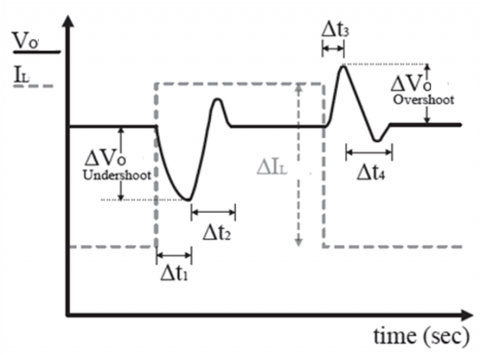
3.3 Transient response analysis
Transient response is the dynamic performance of linear regulator [10]. It can be separated into two parts, one is form load variation, named as load transient response, and the other is from line variation, named as line transient response. A typical LDO regulator transient response to load changes is shown in Figure 9.
For an increase of load current by ΔIL, the LDO output observes an undershoot ΔVO, for a response time duration of Δt1. The loop reacts to this load change and the output voltage settles in a time duration defined by reaction time also known settling time Δt2. Minimizing Δt1+Δt2 is a critical need for digital load applications. The LDO response time Δt1 depends on undershoot ΔVO, output capacitance CO and load current change ΔIL, and can be expressed as:
$\Delta {{t}_{1}}={{C}_{O}}.\frac{\Delta {{V}_{O}}}{\Delta {{I}_{L}}}$ (30)
The settling time, Δt2 is determined by the open-loop bandwidth ωpd of the regulation loop and the slew-rate (SR) at the gate of pass transistor MP and can be written as:
$\Delta {{t}_{2}}=\frac{2\pi }{{{\omega }_{pd}}}+SR$ (31)
with,
$SR={{C}_{G,P}}.\frac{\Delta {{V}_{G,P}}}{{{I}_{SR}}}$ (32)
where, ΔVG,P and ISR represent the voltage change and slewing current at the gate of MP, and we have ΔVG,P is proportional to ΔVO.
The proposed compensation circuit also improves the transient response by increasing the bias current at the gate of the pass transistor MP via the current amplifier block which amplifies this bias current IB,C during the transient times of the load current, which allows to minimize the slew-rate and consequently to reduce overshoots and undershoots and also to reduce the settling time.
Figure 9. Typical LDO Regulator Load Transient Response
3.4 Voltage reference
The LDO regulator proposed in this work also includes the voltage reference, which plays an important role in the accuracy of the feedback voltage VFB, which is why this voltage reference VREF must have a precise value and independent of the temperature, the supply voltage and the process of the technology used. The voltage reference designed for the LDO regulator was previously realized and published by the same authors [32]. The value of VREF is equal to 0.635 V.
The proposed three stage LDO regulator with dual frequency compensation scheme was simulated in standard 0.18 µm CMOS process using Cadence Virtuoso Spectre Simulator.
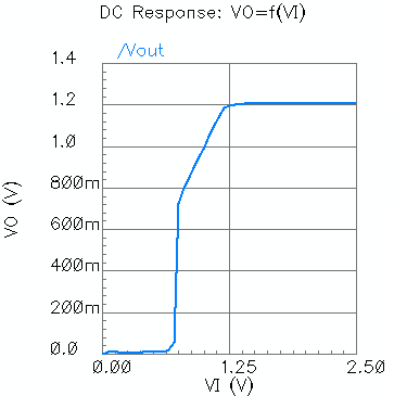
As shown in Figure 10 in the DC line simulation at maximum load current of 150 mA, the proposed LDO provides a DC output voltage VO of 1.2 V from a minimum input supply voltage VI of 1.35 V. The DC line regulation is 4.68mV/V for input supply voltage variation ΔVI of 0.5 V from 1.35 V to 1.85 V, this operating voltage range is limited by the line regulation of the designed voltage reference [32] as shown in Figure 10 (b).
(a) With ideal voltage reference
(b) With internal voltage reference
Figure 10. Simulation result of the DC line regulation at maximum load current
(a) Current efficiency
(b) Power efficiency
Figure 11. Simulation result of efficiency at maximum load current
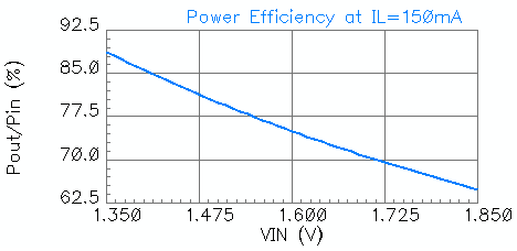
As shown in Figure 11 in the DC efficiency simulation, for VI=1.6, the current efficiency is equal to 99.9662 % while the power efficiency is 75 % at maximum load current of 150 mA, respectively.
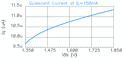
Figure 12 gives the simulation result of the quiescent current. The quiescent current consumed by the proposed LDO regulator in full load condition and under the supply input voltage of 1.6 V is 10.75 µA without voltage reference, while this current is 50.75 µA with the internal voltage reference.
(a) With ideal voltage reference
(b) With Internal voltage reference
Figure 12. Simulation result of quiescent current
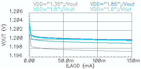
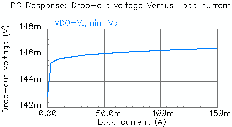
(a) DC load regulation
(b) Drop-out voltage
Figure 13. DC load simulation result
As shown in Figure 13 in the DC load simulation, the DC load regulation is equal to 24.2 µV/mA at VI=1.6 V measured from Figure 13 (a). The proposed LDO regulator has a low value of the drop-out voltage less than 150mV for all required load current range as shown in Figure 13 (b).
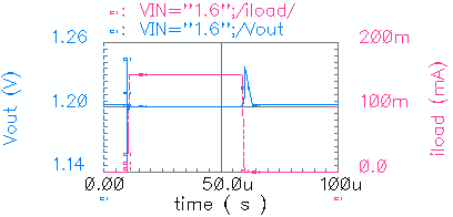
(a) Transient line regulation for IL,max=150 mA
(b) Transient load regulation for VI=1.6 V
Figure 14. Transient simulation
Figure 14 presents the transient simulation of the proposed compensated LDO regulator. As shown in Figure 14 (a), for transient line regulation performed at maximum load current IL,max of 150mA, the output voltage VO presents an overshoot of 19.77 mV when the input supply voltage VI pulse up from 1.35 V to 1.85 V during 1 µs of rise time, while VO presents an undershoot of −17.15 mV when VI pulse down from 1.85 V to 1.35 V during 1 µs of fall time. As shown in Figure 14 (b), for transient load regulation performed at input supply voltage VI of 1.6 V, VO presents an overshoot of 44.9 mV and an undershoot of −50.8 mV when load current pulse up from 0mA up to 150mA during 1 µs of rise time, while VO presents an overshoot of 34.1 mV when load current pulse down from 150mA down to 0mA during 1 µs of fall time.
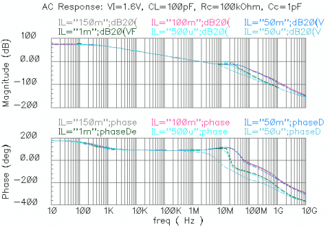
Figure 15 shows the open loop AC simulation for all required load current range at input supply voltage of 1.6V under CL=100pF, RC=100kΩ and CC=1pF. The proposed LDO is stable for all required current load range. The minimum value of load current IL for normal operation is 50 µA. The unity gain frequency is practically constant for any value of IL in the required range and it is close to 1 MHz, which presents a good performance of the proposed compensation circuit. The AC magnitude exhibits a high frequency peak, its location depends on the value of the load current and this due to the presence of two complex conjugate poles as it has been proved in section 3. Table 1 summarizes the AC simulation performance for the proposed LDO regulator at input supply voltage VI of 1.6 V.
Figure 15. AC open loop simulation for all required load current range
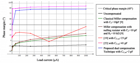
To show the robustness of the proposed dual compensation technique in term of stability with respect to the load current, a comparison with classical compensation methods and others compensation methods cited in this work such as [18] and [21] is performed as shown in Figure 16. The proposed compensation technique ensures stability not only for low values of the load current but also for very low values of the load current, in particular for a zero load current where the phase margin is equal to 45.1° as it is shown in Figure 16 (b). This result is not achieved by the compensation methods proposed in [18, 21]. In addition, the proposed compensation circuit uses a total compensation capacitance CC,tot of 2 pF, while the authors of [18, 21] have used 23 pF and 41 pF respectively to guarantee good stability. The smaller the capacitor to integrate on the chip, the more the layout area is saved.
Table 1. AC simulation performance of the proposed LDO regulator at VI =1.6V
|
Performance |
Mimum load |
Full load |
|
DC gain |H0,c| |
72.53 dB |
74.05 dB |
|
Bandwidth fpd 1 |
268.3 Hz |
220.3 Hz |
|
Gain-bandwidth product |H0,c|. fpd |
1.135 MHz |
1.110 MHz |
|
Unity gain frequency fUGF |
1.139 MHz |
1.113 MHz |
|
Phase margin PM 2 |
84.06° |
92.08° |
|
Resonant frequency fr3 |
6.309 MHz |
39.81 MHz |
1. fpd=2πωpd. 2 PM=180°+Arg[Hol,c(j2πfUGF)]. 3 fr = fpd=2πωr
Table 2 summarizes performance characteristics of the proposed LDO regulator and comparison with others LDO regulators cited in this work is given. For comparison of the State of the Art, some Figures of Merit (FOMs) is proposed [33]. Note that the smaller the FOM chosen for this work, the better the regulator. The FOM chosen for the comparison is given by Eq. (33), where |ΔVO,max| is the maximum variation of the output voltage VO in the line voltage or the load current (maximum overshoot or absolute value of minimum undershoot), IQ is the quiescent current, CL is the load capacitance and IL,max is the maximum load current.
$FOM=\left| \Delta {{V}_{O,\max }} \right|.\frac{{{C}_{L}}.{{I}_{Q}}}{I_{L,\max }^{2}}$ (33)
(a) all load current range
(b) low load current range
Figure 16. Phase margin versus load current for LDO regulator system
Table 2. Performance of proposed LDO regulator and comparison with other LDO regulators cited in this work
|
Performance |
[17] |
[25] |
[26] |
[27] |
[18] |
[22] |
This work |
|
Process (µm) |
0.35 |
0.18 |
0.35 |
0.5 |
0.065 |
0.18 |
0.18 |
|
Input supply voltage VI (V) |
3.0-4.0 |
1.1-1.5 |
1.2-1.5 |
1.4-4.2 |
1.2 |
1.1-1.5 |
1.35-1.85 |
|
Output voltage VO (V) |
2.8 |
1.0 |
1.0 |
1.21 |
1.0 |
1.0 |
1.2 |
|
Drop-Out voltage VDO @ IL,max (mV) |
200 |
100 |
200 |
200 |
200 |
114 |
146.6 |
|
Maximum load current IL,max (mA) |
50 |
50 |
50 |
100 |
100 |
100 |
150 |
|
Quiescent current IQ @ IL,max (µA) |
65 |
54 |
45 |
45 |
82.4 |
20 |
59.68-11.3 649.68-51.3 |
|
Current efficiency ηI @ IL,max (%) |
99.935 |
99.946 |
99.955 |
99.955 |
99.917 |
1N. A. |
99.968-99.967 |
|
Power efficiency η @ IL,max (%) |
1N. A. |
1N. A. |
1N. A. |
1N. A. |
1N. A. |
1N. A. |
88.8-65.5 |
|
Minimum on-chip output capacitance CL (pF) |
102 |
102 |
103 (Off-chip) |
105 (Off-chip) |
102 |
102 |
102 |
|
Total compensation capacitance CC,tot (pF) |
23 |
5 |
41 |
|
|
12 |
2 |
|
Transient Line Regulation (ΔVO varying VI) |
|
||||||
|
Maximum overshoot (mV) |
90 |
1N. A. |
1N. A. |
23 |
8.91 |
55.66 |
23.05 |
|
Minimum undershoot (mV) |
−10 |
1N. A. |
1N. A. |
−12 |
−10.63 |
−55.34 |
−22.49 |
|
Transient Load Regulation (ΔVO varying IL) |
|
||||||
|
Maximum overshoot (mV) |
80 |
100 |
70 |
47 |
0 |
99.52 |
31.1 |
|
Minimum undershoot (mV) |
−80 |
−80 |
-70 |
−48 |
−68.8 |
-591.1 |
−54.5 |
|
2 Response time (µs) |
15 |
2 |
4 |
5 |
6 |
6.3 |
31,697 41,994 |
|
Internal Votlage Reference |
No |
No |
No |
No |
No |
No |
Yes |
|
DC Line Regulation @ IL,max (mV/V) |
1N. A. |
1N. A. |
0.327 |
1N. A. |
4.7 |
1N. A. |
4.68 |
|
DC Load Regulation (µV/mA) |
1N. A. |
1N. A. |
250 |
408 |
300 |
1 |
24.7-24.9 |
|
FOM (fs) |
416 |
388.8 |
2520 |
42750 |
56.69 |
118.2 |
2.345712.03 |
1Not available, 2Value obtained in load transient regulation, 3Simulated value obtained at VI=1.6 V for IL step-up variation from 150 mA to 0 mA with 1 µs of rise time, 4Simulated value obtained at VI=1.6 V for IL step-down variation from 0 mA to 150 mA with 1 µs of fall time, 5 Values obtained with ideal voltage reference, 6 Values obtained with internal voltage reference, 7 Value obtained with internal voltage reference and calculated by using Eq. (32)
It is difficult to compare LDO regulators because generally each one is intended for a specific application. There are always tradeoffs between different performances such as high stability, fast transient response, low quiescent current which increases battery life and high power supply ripple rejection ratio which is not addressed in the proposed work. To determine the good LDO regulator from the performances inserted in Table 2, we base on the calculated value of the figure of merit FOM which includes the consumption from quiescent current, the capability of the LDO regulator to provide maximum current, the capacitance used to the output which must be as small as possible to save the surface and finally the maximum peak of the output voltage which must be minimized to avoid an abnormal operation of the circuit supplied by the LDO regulator. The proposed LDO regulator is better compared with the LDO regulators cited in the Table 2, because it has the smallest value of FOM which is equal to 2.345 fs with ideal voltage reference, while FOM is equal to 12.03 fs with internal voltage reference.
In this paper, a novel internally frequency compensation technique called dual frequency compensation is proposed to enhance stability and transient response of the on-chip output capacitor three stage low-dropout linear voltage regulator. The proposed compensation technique guarantees the stability of the regulator system in a wide range of load current from 0 to 150 mA with small value of compensation capacitance of 2 pF and maximum value of 100 pF of load capacitance. The maximum quiescent current at full load condition of 150 mA is only 51.29 µA when LDO regulator operates with 1.8 V of input supply voltage. Based on the calculated value of the FOM, the proposed LDO regulator exhibits good performance in terms of transient response compared to LDO regulators cited in this paper. The proposed circuit can be used to power a low voltage system on a chip of a smart wearable device. The proposed compensation method in this work degrades the power supply ripple rejection of the LDO regulator due to the decrease in the value of the RG,P resistance. This problem has not been studied in this paper and will be addressed in future work.
[1] Gjanci, J., Chowdhury, M.H. (2011). A hybrid scheme for on-chip voltage regulation in system-on-a-chip (SOC). IEEE Trans. VLSI Syst., 19(11): 1949-1959. http://dx.doi.org/10.1109/TVLSI.2010.2072997
[2] Liu, Q., Shu, W., Chang, J. S. (2017). A 400-MS/s 10-b 2-b/Step SAR ADC With 52-dB SNDR and 5.61-mW Power Dissipation in 65-nm CMOS. IEEE Transactions on Very Large Scale Integration (VLSI) Systems, 25: 3444-3454. http://dx.doi.org/10.1109/TVLSI.2017.2747132
[3] Mehdaoui, Y., El Alami, R. (2018). DSP implementation of the Discrete Fourier Transform using the CORDIC algorithm on fixed point. Advances in Modelling and Analysis B, 61(3): 123-126. http://dx.doi.org/10.18280/ama_b.610303
[4] Mehdaoui, Y., Malaoui, A., Gaga, A., El Alami, R., Mrabti, M. (2019). The efficiency of the CORDIC operator in the MIMO MC-CDMA receiver. Mathematical Modelling of Engineering Problems, 99-104. https://doi.org/10.18280/mmep.060113
[5] Slamti, A., Qjidaa, H. (2011). A high performance regulated charge pump for USB-OTG transceiver. International Conference on Multimedia Computing and Systems. IEEE Xplore Digital Library. http://dx.doi.org/10.1109/ICMCS.2011.5945604
[6] Palumbo, G., Pappalardo, D. (2010). Charge pump circuits: an overview on design strategies and topologies. IEEE Circuits Syst. Mag., 10(1): 31-45. http://dx.doi.org/10.1109/MCAS.2009.935695
[7] Zheng, C., Ma, D. (2010). A 10MHz 92.1%-efficiency green-mode automatic reconfigurable switching converter with adaptively compensated single-bound hysteresis control. IEEE International Solid-State Circuits Conference, pp. 204-205. http://dx.doi.org/10.1109/ISSCC.2010.5433986
[8] Mulligan, M.D., Broach, B., Lee T.H. (2007). A 3MHz Low-voltage buck bonverter with improved light load Efficiency. IEEE International Solid-State Circuits Conference. Digest of Technical Papers, 528-620. http://dx.doi.org/10.1109/ISSCC.2007.373527
[9] Hou, Y.C. (2017). Design of conditioning circuit for weak signal in through-casing resistivity logging. European Journal of Electrical Engineering, 197-208. https://doi.org/10.3166/EJEE.19.197-208
[10] Rincon-Mora, G.A. (2009). Analog IC design with low-dropout regulators (LDOs). 1st edn. The McGraw-Hill Companies, Inc. ISBN: 9780071608930
[11] Shi, C., Walker, B.C., Zeisel, E., Hu, B., McAllister, G.H. (2007). A highly integrated power management IC for advanced mobile applications. IEEE J. Solid-State Circuits, 42(8): 1723-1731. http://dx.doi.org/10.1109/CICC.2006.320982
[12] Annema, A.J., Nauta, B., van Langevelde, R., Tuinhout, H. (2005). Analog circuits in ultra-deep submicron cmos. IEEE J. Solid-State Circuits, 40(1): 132-143. http://dx.doi.org/10.1109/JSSC.2004.837247
[13] Lewyn, L.L., Ytterdal, T., Wulff, C., Martin, K. (2009). Analog circuit design in nanoscale cmos technologies. Proceedings of the IEEE, 97(10): 1687-1714. http://dx.doi.org/10.1109/JPROC.2009.2024663
[14] Patel, A.P., Rincon-Mora, G.A. (2010). High power-supply-rejection (PSR) current-mode low-dropout (LDO) regulator. IEEE Transactions on Circuits and Systems II: Express Briefs, 57(11). http://dx.doi.org/10.1109/TCSII.2010.2068110
[15] Leung, K.N., Mok, P. (2003). A capacitor-free cmos low-dropout regulator with damping-factor control frequency compensation. IEEE J. Solid-State Circuits, 38(10): 1691-1702. http://dx.doi.org/10.1109/JSSC.2003.817256
[16] Leung, K.N., Mok, P. (2001). Analysis of multistage amplifier-frequency compensation. IEEE Transactions on Circuits and Systems I: Fundamental Theory and Applications, 48(9): 1041-1056. http://dx.doi.org/10.1109/81.948432
[17] Lau, S.K., Mok, P., Leung, K.N. (2007). A low-dropout regulator for SoC with Q-reduction. IEEE Journal of Solid-State Circuits, 42(3): 658-664. http://doi.org/10.1109/JSSC.2006.891496
[18] Milliken, R., Silva-Martinez, E., Sanchez-Sinencio, E. (2007). Full on-chip CMOS low-dropout voltage regulator. IEEE Trans. Circuits Syst. I: Regul. Pap., 54(9): 1879-1890. http://dx.doi.org/10.1109/TCSI.2007.902615
[19] Giustolisi, G., Palumbo, G., Spitale, E. (2007). Ldo compensation strategy based on current buffer/amplifiers. 18th European Conference on Circuit Theory and Design: pp. 116-119. http://dx.doi.org/10.1109/ECCTD.2007.4529550
[20] Shen, L.G., Yan, Z.S., Zhang, X., Zhao, Y.F. (2008). A capacitor-less low-dropout regulator for soc with bi- directional asymmetric buffer. IEEE International Symposium on Circuits and Systems, pp. 2677-2680. http://dx.doi.org/10.1109/ISCAS.2008.4542008
[21] Giustolisi, G., Palumbo, G., Spitale, E. (2012). Robust miller compensation with current amplifiers applied to ldo voltage regulators. IEEE Trans. Circuits Syst. I: Regul. Pap., 59(9): 1880-1893. http://dx.doi.org/10.1109/TCSI.2012.2185306
[22] Garimella, A., Rashid, M., Furth, P. (2010). Reverse nested miller compensation using current buffers in a three-stage ldo. IEEE Trans. Circuits Syst. II: Express Br., 57(4): 250-254. http://dx.doi.org/10.1109/TCSII.2010.2043401
[23] Chong, S., Chan, P.K. (2013). A 0.9-/spl mu/A quiescent current output-capacitorless LDO regulator with adaptive power transistors in 65-nm CMOS. IEEE Trans. Circuits Syst. I: Regul. Pap., 60(4): 1072-1081. http://doi.org/10.1109/TCSI.2012.2215392
[24] Carvajal, R., Ramirez-Angulo, J., Lopez-Martin, A., Torralba, A., Galan, J., Carlosena, A., Chavero, F. (2005). The flipped voltage follower: A useful cell for low-voltage low-power circuit design. IEEE Trans. Circuits Syst. I: Regul. Pap., 52(7): 1276-1291. http://dx.doi.org/10.1109/TCSI.2005.851387
[25] Ramirez-Angulo, J., Valero-Bernal, M.R., Lopez-Martin, A., Carvajal, R., Torralba, A., Celma-Pueyo, S., Medrano-Marqués, N. (2013). The flipped voltage follower: Theory and applications. Analog/RF and Mixed-Signal Circuit Systematic Design, chapter 12: 269-287. http://dx.doi.org/10.1007/978-3-642-36329-0_12
[26] Manda, M., Pakala, S.H., Furth, P.M. (2017). A multi-loop low-dropout FVF voltage regulator with enhanced load regulation. IEEE 60th International Midwest Symposium on Circuits and Systems (MWSCAS). http://doi.org/10.1109/MWSCAS.2017.8052847
[27] Tan, X.L., Koay, K.C., Chong, S.S., Chan, P.K. (2014). A FVF ldo regulator with dual-summed miller frequency compensation for wide load capacitance range applications. IEEE Trans. Circuits Syst. I: Regul. Pap., 61(5): 1304-1312. http://doi.org/10.1109/TCSI.2014.2309902
[28] Abdi, F., Bastan, Y., Amiri, P. (2019). Dynamic current-boosting based FVF for output-capacitor-less LDO Regulator. Analog Integrated Circuits and Signal Processing. http://doi.org/10.1007/s10470-019-01479-x
[29] Razavi, B. (2017). Design of Analog CMOS Integrated Circuits. Second edition, by McGraw-Hill Education. ISBN 978-0-07-252493-2
[30] Erickson, R.W., Maksimovic, D. (2020). Fundamentals of Power Electronics. Springer Nature Switzeland. https://doi.org./10.1007/978-3-030-43881-4_21
[31] Nickalls, R.W. (1993). A new approach to solving the cubic: Cardan’s solution revealed. Math. Gazette, 77(480): 354-359. https://doi.org/10.2307/3619777
[32] Slamti, A. Mehdaoui, Y., Chenouni, D., Lakhliai, Z. (2019). A sub-1V high PSRR OpAmp based β-multiplier CMOS bandgap voltage reference with resistive division. Indonesian Journal of Electrical Engineering and Computer Science, 15(1): 155-167. http://dx.doi.org/10.11591/ijeecs.v15.i1.pp155-167
[33] Hazucha, P., Karnik, T., Bloechel, B., Parsons, C., Finan, D., Borkar, S. (2005). Area-efficient linear regulator with ultra-fast load regulation. IEEE J. Solid-State Circuits, 40(4): 933-940. http://dx.doi.org/10.1109/JSSC.2004.842831