Tukur Gupta*![]() | Gaurav Verma
| Gaurav Verma![]() | Shamim Akhter
| Shamim Akhter![]()
© 2023 IIETA. This article is published by IIETA and is licensed under the CC BY 4.0 license (http://creativecommons.org/licenses/by/4.0/).
OPEN ACCESS
The modular adder, a critical arithmetic component for residue calculations, is explored in this study through its implementation on a field programmable gate array (FPGA), specifically targeting the Xilinx Zynq-7000 family device. Recent literature reveals an innovative combination of parallel prefix addition and flagged prefix addition techniques for the design of the modular adder. The parallel prefix addition, an evolution of the carry look-ahead addition, utilizes the prefix operation, whereas the flagged prefix addition generates a novel set of intermediate outputs, namely flag bits, to execute the increment operation. This paper extends this innovative combination by demonstrating the FPGA implementation of the existing design via two distinct strategies. The first strategy employs a register-transfer level (RTL) description of the design using the very high-speed integrated circuit hardware description language (VHDL), while the second strategy deploys user-defined intellectual property (IP) blocks for the design implementation. FPGA area and power reports are subsequently generated using VIVADO IDE. The RTL approach illustrates an average savings of 14.30% in slice look-up tables (LUTs) utilization and 1.91% in slice flip-flops (FFs) utilization, suggesting its superiority for applications that prioritize area-efficiency. However, the IP modeling approach emerges as crucial for managing the perpetually increasing complexity of system-on-chip (SoC) designs.
IP modeling, RTL, area, power, FPGA, modular adder
The modular adder serves as a foundational element in residue number system (RNS) processors, facilitating swift, precise computations [1]. The RNS operates by disassembling a number into components and executing arithmetic operations in parallel, considerably reducing the breadth of carry propagation. Consequently, RNS arithmetic has been proposed as an efficient solution for augmenting the performance of arithmetic hardware. Implementing such intricate designs of very large-scale integration (VLSI) circuits can be realized through various methodologies.
The need for integrating millions of gates in contemporary VLSI systems, operating within the Giga-Hertz (GHz) range, has necessitated the reuse of intellectual property (IP) for circuit design [2]. This need stems from the substantial reduction in design complexity and design time, and consequently, time to market, when pre-designed and tested IPs are integrated. IPs can be conceptualized as blocks of logic utilized in a semiconductor chip to create field-programmable gate arrays (FPGAs) and application-specific integrated circuits (ASICs). Whereas an FPGA is a reprogrammable integrated circuit, an ASIC is a specialized kind of integrated circuit tailored for a specific application.
Within the semiconductor industry, an IP core is a reusable unit of logic or functionality, a module, or a layout scheme often created with the intention of licensing to multiple vendors for use as building blocks in various chip designs. These IP blocks, optimized for area and power in an FPGA driven by specific technology, follow a definite process for generation, enabling their use as reusable components. The adoption of IP modeling methodology enables the integration and reuse of IP components at any stage of the design process, allowing the validation of system functionality and its characteristics at each stage.
Contrastingly, register-transfer level (RTL) design is predicated on generating hardware description language (HDL) descriptions for the complete design, followed by simulation and synthesis. Here, complex hardware specifications are translated into VHDL or Verilog. The target circuit is accurately and formally described using a hardware description language, enabling automatic analysis and modeling of an electronic circuit. Functional verification is conducted in addition to the digital implementation to ensure that the RTL design is in accordance with the specifications. The RTL is transformed into a gate-level netlist once all the blocks have been implemented and confirmed.
This paper aims to execute the FPGA design and implementation of the generic modular adder using both the aforementioned design approaches. The architecture of the generic modular adder explored in this paper has been recently presented in the study of Gupta and Akhter [3]. This work expands upon the idea of implementing a similar architecture on the latest Zynq family FPGA device using two different approaches, namely, RTL programming and IP modeling. By replicating and synthesizing the design on an available FPGA chip, the authors affirm the originality of this paper. In contrast, the same design was synthesized using unit gate models and electronic design automation (EDA) tools based on the ASIC design processes in the published study of Gupta and Akhter [3].
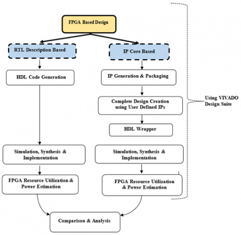
The paper is structured into five main sections. Section 2 reviews relevant existing literature. Section 3 provides a detailed account of the design of the generic modular adder, which is subsequently implemented on FPGA using RTL programming and IP modeling approaches in Section 4. Section 5 presents a comparative analysis of FPGA resource utilization and total power dissipation for both cases. This is followed by the conclusion and future scope in Section 6. Figure 1 illustrates the sequence of the events undertaken in this paper.
Figure 1. Roadmap of the proposed work
Extensive research has been undertaken on various digital systems for their field-programmable gate array (FPGA) implementation, as well as for the estimation of FPGA area and power. A selection of these significant contributions is discussed herein. The state of the art relating to the FPGA implementation of various digital systems is described in several pieces of literature [4-18], and a summary is provided in Table 1.
Rogawski et al. [4] employed four different FPGA devices to implement novel designs of parallel prefix adders and modular adders. The area and delay results for all four devices were analyzed. Concurrently, Kharadkar et al. [5] implemented a specific modular adder on the Spartan-III FPGA device, examining three vital parameters: area, power, and delay for the adder designs. In both instances, the register-transfer level (RTL) coding methodology was utilized for the design.
A Montgomery algorithm-based modular multiplier was implemented on a Virtex-6 FPGA device using embedded IP cores by Yang et al. [6]. Similarly, Ajit et al. [7] used a Virtex-6 FPGA device to implement RTL coding-based designs of several popular adder topologies. In this instance, the trade-offs between area, power, and delay were studied.
Several pieces of literature discuss the IP core-based designing of essential digital systems and their implementation on contemporary FPGA devices [8-12]. Billmann et al. [8] conducted a comprehensive evaluation of the available open-source crypto IP cores. Yaman et al. [9] presented a real-time edge detecting system based on custom IP cores, implemented on a Digilent Basys3 FPGA board. The algorithm principle of RSA was studied in detail by Liu [10], and an FPGA implementation of an RSA IP core was verified on the latest Zynq family device. Additionally, the resource utilization and throughput of the target designs were analyzed.
Tolba et al. [11] presented Memristor IP cores synthesized and validated on an Artix-7 FPGA device. Singh et al. [12] proposed IP modeling-based power models for a 4-tap FIR filter, with designs synthesized and validated on the latest Zynq family FPGA device.
Akhil et al. [13] implemented an 8-point radix-2 DIT FFT on a Zynq family FPGA device, using the conventional approach of RTL coding. Singh et al. [14, 15] proposed additional IP core-based digital systems, with designs synthesized and validated on the latest Zynq family FPGA devices. Modulation systems and ADC IP cores were implemented by Singh et al. [14, 15] respectively.
Coliban [16] made a significant contribution to the field of Montgomery multiplication, using the RTL coding methodology. In a similar vein to the study of Singh et al. [12], Singh et al. [17] proposed IP modeling-based power models for DSP blocks. Lastly, Huang [18] proposed a novel design and implementation of an IIC interface IP core, claiming reduced resource utilization with a complete range of functions, compared to existing similar IP cores.
Table 1. Investigation of State-of-the-Art FPGA implementation of diverse digital circuits designed using RTL programming and IP modeling methodologies
|
S. No. |
[Reference] (Year) |
Target FPGA Device |
Design Methodology Used (RTL Code/ IP Core) |
Target Blocks/ Circuits |
Design/ Performance Metrics Investigated |
Significant Findings |
|
1 |
[4] (2014) |
65nm Altera Stratix III, Xilinx Virtex 5, 40nm Altera Cyclone IV, 45nm Xilinx Spartan 6 |
RTL coding |
Parallel prefix network adders & Modular adders |
Area, delay |
Proposed low-latency family of high-radix Parallel Prefix Network adders and modular adders outperform the traditional PPN adders in terms of all performance measures |
|
2 |
[5] (2015) |
Xilinx Spartan3-xc3s1000 FPGA device |
RTL coding |
modulo (231-1) adder architecture |
Area, power , delay |
The proposed architecture offers savings in area & power, and improves speed |
|
3 |
[6] (2016) |
Virtex-6 FPGA device |
IP core |
Modular multiplication design |
Delay, resource utilization |
The proposed scheme can achieve 256 ×256 bits multiplication using available multiplier IP cores |
|
4 |
[7] (2019) |
Virtex-6 FPGA device |
RTL coding |
Different adder topologies |
Area, power, delay |
Trade-offs between area, power and delay vary with different adder topologies |
|
5 |
[8] (2019) |
Zynq-Z7010 chip |
IP core |
Open-source Crypto IP cores |
Bandwidth, resource utilization |
Available cryptographic IP cores are analysed |
|
6 |
[9] (2019) |
Digilent Basys3 FPGA board |
IP core |
Sobel Filter design |
Resource utilization |
The proposed design offers high accuracy and low area resource utilization |
|
7 |
[10] (2019) |
Zynq family xc7vx485 FPGA device |
IP core |
RSA IP |
Resource utilization, throughput |
The proposed IP core offers savings in area and claims higher throughput |
|
8 |
[11] (2019) |
Nexys 4 Artix-7 FPGA XC7A100T |
IP core |
Memristor models |
Resource utilization, frequency, throughput |
Designed IP core offers low area utilization and high speed with higher degree of controllability |
|
9 |
[12] (2020) |
Zynq family (xc7z020clg484-1) FPGA device |
IP core |
4-tap FIR filter |
Power |
Proposed power models outperforms as compared to the most competitive work in literature |
|
10 |
[13] (2020) |
ZYNQ board |
RTL coding |
8-point Radix-2 DIT (Decimation In Time) FFT |
Area, delay |
8-point FFT (Using Floating point multiplier incorporated with CORDIC multiplier and KSA) is the most optimized combination |
|
11 |
[14] (2021) |
Zynq family (xc7z020clg484-1) FPGA device |
IP core |
QPSK & BPSK Modulation systems |
Power |
Proposed power models outperforms in power estimation of complete systems |
|
12 |
[15] (2021) |
Zynq family (XC7Z045FFG900-0I) FPGA device |
IP core |
ADC soft IP core |
Throughput, accuracy |
Developed IP supports multiple configurations |
|
13 |
[16] (2022) |
Virtex-7 FPGA device |
RTL coding |
radix-2 Montgomery multiplication architecture |
Time, area |
Notable improvement in multiplication time, throughput and maximum operating frequency |
|
14 |
[17] (2022) |
Zynq family (xc7z020clg484-1) FPGA device |
IP core |
DSP Blocks |
Power |
Power models of individual IPs are created |
|
15 |
[18] (2023) |
All FPGA devices |
IP core |
IIC (Inter-Integrated Circuit) Interface |
(No parameters analysed) |
IIC Interface IP core is designed |
|
16 |
Proposed |
Zynq family (xc7z020clg484-1) FPGA device |
Both RTL code & IP core |
Modulo adder with modulus of form (2n-K) |
Area, Power |
A novel work presenting the comparison of both the design methodologies |
Notably, no resources within the literature surveyed in the present work provide an empirical comparison of different design methodologies adopted for system-on-chip (SOC) implementations. This paper, however, extends the preceding work found in the study of Gupta et al. [3] by designing a modulo 2n-K adder using two distinct methodologies and implementing the resultant design on an FPGA.
In a novel approach, this paper also conducts a comparative analysis of both methodologies in terms of FPGA resource utilization and power dissipation of the designed modular adder. These analyses are comprehensively detailed in Sections 4 and 5. This contribution fills a recognized gap in the existing body of knowledge by providing empirical comparisons between different SOC design methodologies, an aspect that was previously unaddressed in the literature.
In the following discussion, a brief overview of the digital circuit, presented in previous work [3] is given, thereby forming a sufficient background to understand the investigated digital system i.e. generic modular adder. Gupta and Akhter [3] discussed a novel design of generic modulo adder for moduli of the form (2n-K) where K is any integer in the range $3 \leq K \leq\left(2^{\mathrm{n}-1}\right)$. The adder design uses parallel prefix addition in first stage and flagged prefix addition in second stage. One of the quickest adders is the parallel prefix adder (PPA), which is a modified version of the carry lookahead (CLA) adder. High performance arithmetic processors employ a tree structure, which is the foundation for PPAs. The PPA structure's addition operation is completed with three steps; pre-processing, prefix and post-processing operation [23]. Flagged prefix adder is obtained by incorporating basic hardware for calculating a new set of bits termed flag bits [24].
As claimed by the authors, the presented design of modulo adder offers reduced area and power dissipation when compared with the most recent and competitive literature. Both the addition techniques are briefly reviewed in following subsection.
To begin with, it is important to understand the concept of modular addition, specifically for the moduli of the form (2n-K), as mentioned above.
Modular addition i.e. $\langle x+y\rangle_m$ where x and y are two numbers (lying between 0 and m-1) and m is the modulus of any form, is given by the expression in Eq. (1) [25]:
$\langle x+y\rangle_m=\left\{\begin{array}{ll}x+y & \text { if } x+y<m \\ x+y-m & \text { if } x+y \geq m\end{array}\right\}$ (1)
Modular adders, according to the form of moduli are broadly classified as specific modular adders and generic modular adders. Using generic moduli forms in modular adders allows higher level of parallelism in arithmetic structures and thereby claiming improved performance of RNS processors over specific moduli based systems. The previous work [3] and the present paper focus on the generic modulo adder with moduli of the form (2n-K). The expression for the target modular addition is given by
$S_{\mathrm{Mod}}=\langle A+B\rangle_m$ (2)
where, $m=\left(2^n-K\right)$ and $3 \leq K \leq 2^{n-1}$.
Expanding and rearranging the terms in above expression Eq. (2) gives
$S_{\mathrm{Mod}}=\left\{\begin{array}{ll}\langle A+B\rangle_{2^n} & \text { if } C_{\text {out }}=0 \\ \langle A+B+K\rangle_{2^n} & \text { if } C_{\text {out }}=1\end{array}\right\}$ (3)
Output carry, $C_{\text {out }}$ is the resultant carry obtained by computing $(A+B+K)$.
Gupta and Akhter [3] have implemented the expression Eq. (3) in two stages where first stage uses parallel prefix addition followed by flagged prefix addition in second stage. These two are the classic approaches which have been revised and applied in the adder design [24-26]. However, literature [3] is confined to design flow based EDA tools rather than using more flexible and reconfigurable FPGA technology.
The novelty in the present work lies in the fact that above modular adder design has been reproduced and synthesized using latest FPGA device from Zynq family. Also two different design methodologies, namely RTL Programming and IP modeling are adopted and analyzed for the same architecture as discussed in subsequent sections. The acquisition and usage of IP Cores has replaced the design of HDL modules as the primary focus of contemporary FPGA development. System on Chip (SoC) designs frequently incorporate IP Cores because they may be used as building blocks to accelerate development while lowering risk. Since the year 2000, the use of IP Cores in chip design has grown significantly. Today, there are over 100 businesses that create and market IP cores for use in analog, digital, RF, and other fields. Hence, both the methodologies need to be explored for design prospects.
This paper extends the work presented in recent literature by employing IP modeling approach to design the modular adder along with the conventional method of RTL programming [3]. Both the methodologies have been detailed in this section.
4.1 RTL (Register-Transfer Level) description based design
A number of tactics can be followed to write an HDL code for implementing a specific design on FPGA. Every FPGA has fixed hardware specification including number of memory elements, input-output banks and configurable logic blocks (CLBs) comprising of look-up tables (LUTs), flip-flops (FFs) and multiplexers [26]. Therefore, number of resources used by a design depends on the way of implementing the logic supporting the design, i.e. the HDL coding strategy followed to implement the design. RTL description methodology presents conventional design approach as demonstrated in Figure 2.
Figure 2. RTL programming approach of design creation using Vivado design suite
This approach starts with functional specification followed by HDL code generation (Very High-Speed Hardware Description Language i.e. VHDL in the present work) for the complete design under consideration. This code undergoes simulation for functional verification. After this step, synthesis (with timing constraints) is performed to estimate the resource utilization. Finally, FPGA implementation takes place, where post-implementation area and power reports can be obtained. In this paper, using this methodology, generic modular adder i.e. modulo (2n-K) adder is implemented for input vector length, n = 7, 9, 11, 13, 15 [3]. The RTL schematic for RTL programming based 7-bit modular adder design is shown in Figure 3.
Figure 3. RTL schematic of RTL programming based design of 7-bit modulo (2n-K) adder
4.2 IP (Intellectual Property) core based design
As mentioned in previous section, IP cores or IP blocks are predesigned, independent and reusable modules or subcircuits that can be used to implement larger designs. The IP Packager by Vivado featuring design reuse allows Vivado end user to package the design at any desired level of design flow. With the provision of IP-centric design flow by Vivado Design Suite, any designs and algorithms can be turned into reusable IPs. In Vivado IP catalog, IPs can be consolidated from different sources including Xilinx IPs, third party IPs and end-user designs based IPs. Therefore, IPs can be classified under two broad categories, i.e., embedded IPs, available in vendor library and user-defined IPs. Embedded IPs is another name for built-in IP made available in the library or repository by the vendor. However, programmers can design their own IPs according to the target design and reuse them for designing the complex architectures with ease. Such IPs are termed as user-defined IPs. In this paper, modulo adder has been designed using user-defined IPs at RTL level. The process starting from creation and packaging of IPs to creation of full design and estimation of performance parameters has been divided into two phases as shown in Figure 4(a) and Figure 4(b) [10].
(a) Phase-I demonstrating IP creation and packaging
(b) Phase-II demonstrating complete design creation using IPs created in phase-I
Figure 4. Two-phase IP modeling approach of design creation using Vivado design suite
Figure 5. User-defined IP blocks created and packaged using Vivado design suite
Figure 6. Created block design of the 7-bit modulo (2n-K) adder using user-defined IPs
Figure 7. RTL Schematic of IP modeling based design of 7-bit modulo (2n-K) adder
Phase-I explains the flow of IP packaging, which is shown in Figure 4(a). Functional specification is determined for each IP module followed by project initialization. VHDL is used to generate code for user-defined IPs. Code for IP is simulated for functional verification using commercial tool i.e., Vivado Design Suite. Design synthesis is performed to estimate resource utilization if required. Finally, Vivado IP packager is used to create and package IP. In this paper, using the methodology adopted in phase-I, seven IP blocks have been created and packaged as shown in Figure 5. Phase-II demonstrates the process of full design creation using desired user-defined IPs created in phase I. The flow of design creation is shown in Figure 4(b). During this phase, under the tab ‘Create Block Design’ of Vivado Design Suite, desired IPs are instantiated in the window and target design is created by making interconnections according to the design. Using HDL Wrapper, HDL code is automatically generated according to created design. This code is then simulated and functionality is verified. After this, synthesis is performed followed by implementation (including timing and implementation constraints). Finally, area and power reports can be obtained for implemented design.
The user-defined IPs created in this work for the target design of modular adder are shown in Figure 5. In total, seven IP blocks are created namely, preprocess_v1_0, grey_cell_v1_0, black_cell_v1_0, Rhombas_cell_v1_0, Flag_generate_v1_0, Carry_out_v1_0 and Final_sum_v1_0.
In this paper, using these IPs, generic modular adder i.e. modulo (2n-K) adder is designed for input vector length, n = 7, 9, 11, 13, 15 [3]. The complete block design of 7-bit generic modular adder created using user-defined IPs is shown in Figure 6. The corresponding RTL schematic for the IP modeling based 7-bit modular adder design is shown in Figure 7.
Section 4 in this paper illustrates the designing of modulo (2n-K) adder using two different methodologies, i.e. RTL programming and IP modeling. After describing complete designs using VHDL for input vector length ranging from 7 bits to 31 bits, designs are synthesized and implemented on FPGA targeted to latest device (xc7z020clg484-1) from Zynq family using Vivado tool. Area reports and power reports of the implemented designs are extracted from Vivado tool. Information about hardware specifications of the target FPGA device have been tabulated in Table 2, which helps in understanding the percentage utilization of FPGA resources by the designs under investigation. The proposed work considers a generic modular adder. The use of generic moduli permits lower word length channels, resulting in better parallelism and quicker operations. However, the proposed investigation is confined to the moduli of the form (2n-K). The fact that any moduli may be expressed using this form gives this class of modulo adders a clear benefit. Any advancement in this family of adders opens the door to higher order moduli sets, which boosts parallelism in RNS applications. This study presented in the proposed work can be applied to others other forms of generic modulo adders too.
Significant findings from area report include information on number of LUTs and FFs. These form the basic building blocks of FPGA and hence determine the resource utilization or in other words, total chip area occupied by the implemented design. Factors affecting the power consumption of FPGAs include circuit complexity, clock frequency, interconnects, supply voltage, switching frequency and load capacitance. Frequency considered for this work is 125 MHz. Total on-chip power is obtained by the summation of static power and dynamic power. Static power, i.e. the leakage power is fixed for a particular FPGA family (120 mW in case of zynq family considered for this work). Dynamic power is determined by aggregation of input/output power, signal power, logic power and clock power, where first power segment is the function of LUTs and FFs, while other three segments are not reliant on the area occupancy.
Significant findings from area and power reports have been recorded in Table 3. Also, table gives major insights into the difference between these reports for two design methodologies adopted in this paper for designing modular adder. It is evident from the table that differences may be observed between number of slice LUTs, number of slice FFs and total on-chip power when both the methodologies (RTL programming and IP modeling) are compared. It can be observed from the table 3 that RTL methodology offers an average of 14.30% savings in slice LUTs utilization and 1.91% savings in slice FFs utilization. Though not significant, however perceivable savings are offered in case of total on-chip power as well. This comparison can be better understood from the Figures 8-10.
Table 2. Hardware specification of FPGA used for implementing designs
|
S. No. |
FPGA Features |
Hardware Description |
|
1 |
FPGA Used |
Zed Board Zynq Evaluation and Development Kit (xc7z020clg484-1) |
|
2 |
No. of Slice LUTs (available) |
53200 |
|
3 |
No. of Slice Registers (available) |
106400 |
|
4 |
No. of IO (available) |
202 |
|
5 |
No. of Clocking (available) |
32 |
|
6 |
No. of DSPs (available) |
220 |
Table 3. Comparison of RTL programming and IP modeling approaches for proposed modular adder design in terms of FPGA resource utilization and total on-chip power
|
Input Vector Length (Modulus) n (2n-K) |
Number of Slice LUTs |
Number of Slice FFs |
Total On-Chip Power (mW) |
|||
|
RTL Description Based Design |
IP Modeling Based Design |
RTL Description Based Design |
IP Modeling Based Design |
RTL Description Based Design |
IP Modeling Based Design |
|
|
7 (83) |
51 |
60 |
64 |
66 |
128 |
128 |
|
9 (264) |
72 |
84 |
90 |
92 |
131 |
131 |
|
11 (1170) |
90 |
105 |
113 |
115 |
133 |
134 |
|
13 (5181) |
111 |
129 |
139 |
141 |
136 |
137 |
|
15 (17767) |
129 |
150 |
162 |
164 |
138 |
139 |
Figure 8. Number of slice LUTs utilized by modular adder designed using RTL and IP modeling approach
Figure 9. Number of slice FFs utilized by modular adder designed using RTL and IP modeling approach
Figure 10. Total on-chip power consumed by modular adder designed using RTL and IP modeling approach
With an aim to present more clear view of the comparative analysis performed, differences between both the approaches are graphically presented in terms of LUTs, FFs and total power dissipation in Figures 8-10 respectively. This provides a better perception for presented methodologies. The reduction in FPGA resource utilization and total power in case of RTL approach owes to the fact that designing any target architecture using predefined IP blocks introduces certain redundancy in terms of slice FFs and LUTs in order to accommodate redundant logic functions. While designing the architecture using conventional RTL programming approach, designers or programmers may get an extra scope of preventing unnecessary redundancy being introduced in the design. This is because any efficient strategy can be followed to write HDL code for implementing the logic and FPGA resource allocation vary with this logic supporting the target design. RTL approach may sometimes seem complex because it demands exhaustive knowledge of the components functionality and interconnections. However, it prevents hardware redundancy and hence reduces FPGA resources utilization. This in turn effects the total on-chip power as well. Therefore, RTL methodology of designing is a promising candidate for area and power efficient applications such as modulo adders for RNS based designs. However, chip development cycles are short in today's competitive climate. Hence, design teams often reuse semiconductor IP cores to shorten time to market. In the semiconductor sector, locating IP reuse techniques and possibilities is frequently a top business objective since it may improve processes and save needless rework.
FPGAs and SoCs have made significant advancements during the past two decades. The first cause is the introduction of new silicon process nodes, which allowed engineers to pack more transistor into a given space, and the second is the development of improved EDA tools, which enabled designers to create complicated and massive designs and translate them into SOCs effectively. Furthermore, there was a rise in demand for chips with greater features. As a result, the circuit design flow grew lengthier and more complex, placing a significant load on designers. Therefore, reusable logic blocks i.e., IP cores were designed to address the issues of complicated ICs and lengthier design cycles so that engineers could concentrate their efforts on their core creative technology, which is what truly matters. This work presents implementation and analysis of two design methodologies i.e. RTL programming and IP modeling. Generic modular adder design i.e. modulo (2n-K) adder, existing in the recent literature forms the perfect base for the practical investigation performed in this work [3]. RTL approach prevents any hardware redundancy from being introduced in the design and thereby reducing area and power. Modulo (2n-K) adder, when designed using RTL approach offers average savings of 14.30%, 1.91% and 0.5% in LUTs, FFs and total on-chip power respectively as compared to IP blocks based designs. However, the later approach reduces the design complexity for designers by providing reusable IPs and hence reduces time-to-market. Therefore, this paper presents a novel work of investigation on design approaches, providing comparable results, which forms the strong basis for the further research to be carried out in the field of efficient modular adder designs.
However, in the proposed work, study of both the design methodologies has been narrowed to the generic modular adder with moduli of the form (2n-K). Any improvement to this class of adders promotes the parallelism of RNS applications by enabling higher order moduli sets with improved moduli balancing. There is, nevertheless, a dearth of literature on generic moduli adders. The generic moduli-based adder designs that are now in use have a lot of room for study and development. As a result, significant efforts must be made to improve generic moduli-based modular adder designs. Hence, there is a scope of research in design techniques as discussed in the present work. Also, apart from the design approaches discussed in the present work, another design technique i.e. high-level synthesis (HLS), also known as C synthesis, is an automated design process that takes an abstract behavioral specification of a digital system and finds a register-transfer level structure that realizes the given behavior. By increasing the level of abstraction, it can assist in reducing the design time and cost of VLSI systems. HLS may also adapt the system to a variety of restrictions, including size, power and performance. Hence, high level synthesis has scope of research and investigation for achieving improved circuit design flow.
[1] Omondi, A.R., Premkumar, A.B. (2007). Residue Number Systems: Theory and Implementation (Vol. 2). World Scientific.
[2] Chen, W., Ray, S., Bhadra, J., Abadir, M., Wang, L.C. (2017). Challenges and trends in modern SoC design verification. IEEE Design & Test, 34(5): 7-22. https://doi.org/10.1109/MDAT.2017.2735383
[3] Gupta, T., Akhter, S. (2021) Design and implementation of area-power efficient generic modular adder using flagged prefix addition approach. In International Conference on Signal Processing and Communication (ICSC), Noida, India, pp. 302-307. https://doi.org/10.1109/ICSC53193.2021.9673363
[4] Rogawski, M., Homsirikamol, E., Gaj, K. (2014). A novel modular adder for one thousand bits and more using fast carry chains of modern FPGAs. In: International Conference on Field Programmable Logic and Applications (FPL), Munich, Germany, pp. 1-8. https://doi.org/10.1109/FPL.2014.6927493
[5] Kharadkar, R.D., Hulle, N.B. (2015). FPGA Implementation of Modulo (231-1) Adder. In International Conference on Emerging Trends in Engineering & Technology (ICETET), Kobe, Japan. pp. 85-90. https://doi.org/10.1109/ICETET.2015.23
[6] Yang, Y., Wu, C., Li, Z., Yang, J. (2016). Efficient FPGA implementation of modular multiplication based on Montgomery algorithm. Microprocessors and Microsystems, 47(A): 2019-215. https://doi.org/10.1016/j.micpro.2016.07.008
[7] Ajit, A., Arathi, P.V., Haridas, K., Nambiar, N.M., Devi, S. (2019). FPGA based performance comparison of different basic adder topologies with parallel processing adder. In International Conference on Electronics, Communication and Aerospace Technology (ICECA), Coimbatore, India, pp. 87-92. https://doi.org/10.1109/ICECA.2019.8821925
[8] Billmann, M., Werner, S., Höller, R., Praus, F., Puhm, A., Kerö, N. (2019). Open-source crypto ip cores for fpgas–overview and evaluation. In 2019 Austrochip Workshop on Microelectronics (Austrochip), Vienna, Austria, pp. 47-54. https://doi.org/10.1109/Austrochip.2019.00020
[9] Yaman, S., Karakaya, B., Erol, Y. (2019). Real time edge detection via IP-core based Sobel filter on FPGA. In International Conference on Applied Automation and Industrial Diagnostics (ICAAID), Elazig, Turkey, pp. 1-4. https://doi.org/10.1109/ICAAID.2019.8934964
[10] Liu, B. (2020). Research and implementation of RSA IP core based on FPGA. In Data Processing Techniques and Applications for Cyber-Physical Systems (DPTA 2019), pp. 1311-1319. https://doi.org/10.1007/978-981-15-1468-5_154
[11] Tolba, M.F., Fouda, M.E., Hezayyin, H.G., Madian, A.H., Radwan, A.G. (2018). Memristor FPGA IP core implementation for analog and digital applications. IEEE Transactions on Circuits and Systems II: Express Briefs, 66(8): 1381-1385. https://doi.org/10.1109/TCSII.2018.2882496
[12] Singh, N., Verma, G., Khare, V. (2020) Power Estimation of FIR Filter based on IP Modeling for DSP and Communication Applications. In: Global Conference on Wireless and Optical Technologies (GCWOT), Malaga, Spain, pp. 1-7. https://doi.org/10.1109/GCWOT49901.2020.9391608
[13] Akhil, R., Koleti, J.R., Bhaskar, A.V., Sathish, V., Goud, B.A. (2020). Delay and Area analysis of hardware implementation of FFT using FPGA. In 2020 IEEE International Conference on Electronics, Computing and Communication Technologies (CONECCT), Bangalore, India, pp. 1-6. https://doi.org/10.1109/CONECCT50063.2020.9198617
[14] Singh, N., Verma, G., Khare, V. (2021). Power estimation of QPSK and BPSK modulation systems for FPGAS based on IP modeling for wireless applications. https://doi.org/10.21203/rs.3.rs-538571/v1
[15] Suresh, A., Shyama, S., Srivastava, S., Ranjan, N. (2021) Multichannel ADC IP Core on Xilinx SoC FPGA. In: CS&IT Conference proceedings, 11(23): 341-353. https://doi.org/10.5121/csit.2021.112326
[16] Coliban, R.M. (2022). Fast Radix-2 Montgomery modular multiplication on FPGA using ternary adder. In 2022 International Conference on Computing, Electronics & Communications Engineering (iCCECE), Southend, United Kingdom, pp. 1-5, https://doi.org/10.1109/iCCECE55162.2022.9875097
[17] Singh, N., Verma, G., Khare, V. (2022) Accurate power estimation identity for DSP blocks targeted to FPGAs. Ingénierie des Systèmes d’Information, 27(4): 539-548. https://doi.org/10.18280/isi.270403
[18] Huang, J. (2023) Design and Implementation of IIC Interface IP Core. Academic Journal of Science and Technology, 5: 208-211. https://doi.org/10.54097/ajst.v5i1.5634
[19] Jaberipur, G., Parhami, B., Nejati, S. (2011). On building general modular adders from standard binary arithmetic components. In 2011 Conference Record of the Forty Fifth Asilomar Conference on Signals, Systems and Computers (ASILOMAR), Pacific Grove, CA, USA, pp. 6-9. https://doi.org/10.1109/ACSSC.2011.6189975
[20] Matutino, P.M., Pettenghi, H., Chaves, R., Sousa, L. (2012). RNS Arithmetic Units for Modulo {2^ n+-k}. In 2012 15th Euromicro Conference on Digital System Design, Cesme, Turkey, pp. 795–802. https://doi.org/10.1109/DSD.2012.114
[21] Ma, S., Hu, J.H., Wang, C.H. (2013). A novel modulo 2n-2k-1 adder for residue number system. IEEE Transactions on Circuits and Systems I: Regular Papers, 60(11): 2962-2972. https://doi.org/10.1109/tcsi.2013.2252639
[22] Hiasat, A. (2018). General modular adder designs for residue number system applications. IET Circuits, Devices & Systems, 12(4): 424-431. https://doi.org/10.1049/iet-cds.2017.0470
[23] Bayoumi, M., Jullien, G., Miller, W. (1987). A VLSI implementation of residue adders. IEEE Transactions on Circuits and Systems, 34(3): 284-288. https://doi.org/10.1109/TCS.1987.1086130
[24] Kang, S.M., Leblebici, Y. (2003). CMOS Digital Integrated Circuits. New York: MacGraw-Hill.
[25] Brent, Kung. (1982). A regular layout for parallel adders. IEEE Transactions on Computers, 100(3): 260-264. https://doi.org/10.1109/TC.1982.1675982
[26] Dave, V., Oruklu, E., Sanii, J. (2006) Design and synthesis of flagged binary adders with constant addition. In 2006 49th IEEE International Midwest Symposium on Circuits and Systems, San Juan, PR, USA, pp. 23-27. https://doi.org/10.1109/MWSCAS.2006.381985