Muslimin*![]() | Muh. Ainul Muslim
| Muh. Ainul Muslim![]() | Muh. Fiailal Muslim
| Muh. Fiailal Muslim![]()
© 2025 The authors. This article is published by IIETA and is licensed under the CC BY 4.0 license (http://creativecommons.org/licenses/by/4.0/).
OPEN ACCESS
Indium tin oxide (ITO) is considered one of the most intriguing physical materials for investigation. The properties of ITO materials are strongly influenced by the deposition technique and post-deposition treatment. ITO thin films were deposited by DC sputtering, with the oxygen partial pressure during deposition varied and different annealing temperatures applied to the samples. X-ray analysis revealed that all samples exhibited a maximum orientation along the (400) plane. Structural analysis showed that the lattice constants ranged from 10.17 to 10.25Å, while the grain sizes ranged from 109.10 nm to 122.81 nm. Both lattice constants and grain sizes were found to decrease with increasing oxygen partial pressure and annealing temperature. Electrical resistivity, carrier density, mobility, and bandgap were also observed to change with higher oxygen partial pressure and annealing temperature. Carrier density was found to range from (2.77-6.89)×10²⁰ cm⁻³, mobility from 19.63–32.98 cm²V⁻¹s⁻¹, bandgap from 3.78 eV– 4.30 eV, and resistivity from (3.67–9.7)×10⁻⁴ Ω cm, with the lowest resistivity achieved at an oxygen partial pressure of 3.70% and an annealing temperature of 250℃. Optical properties were also found to change, including refractive index (2.09–2.25), extinction coefficient (2.93–3.49), absorption coefficient (0,036–0.072), and transmittance (81.94%–87.12%). The highest transmittance was observed at an oxygen partial pressure of 8.90% with an annealing temperature of 250℃.
oxygen partial pressure, annealing structure, electrical and optical properties
Indium tin oxide (ITO) is widely recognized as a transparent conducting oxide (TCO) material extensively used in optoelectronic devices such as touch screens, solar cells, and light-emitting diodes. This material exhibits a unique combination of high optical transparency in the visible spectrum and good electrical conductivity. Both characteristics are strongly influenced by fabrication conditions, particularly the oxygen partial pressure during deposition and the annealing treatment following layer formation.
The oxygen partial pressure during the deposition process plays a critical role in controlling the concentration of oxygen vacancies within the ITO crystal structure. These oxygen vacancies act as electron donors, increasing the free charge carrier concentration and thereby reducing the resistivity of the layer. However, excessive electron concentration can reduce optical transmittance due to increased free carrier absorption [1]. Therefore, the regulation of oxygen partial pressure is key to achieving a balance between electrical conductivity and optical transparency.
Moreover, annealing treatment significantly contributes to the crystal structure and functional properties of ITO layers. Annealing performed at appropriate temperatures and atmospheres enhances crystallinity, reduces structural defects, and improves intergrain connectivity, all of which positively affect carrier mobility and optical transparency [2]. Conversely, excessively high annealing temperatures or unsuitable atmospheres may cause structural degradation and performance deterioration [3].
A comprehensive understanding of the effects of oxygen partial pressure and annealing treatment is essential for optimizing the electrical and optical properties of ITO thin films. Research in this area supports not only the enhancement of optoelectronic device efficiency but also the development of functional material technologies based on TCOs.
The electrical properties of In₂O₃: SnO₂ (ITO) thin films are strongly influenced by deposition parameters and the crystallinity of the resulting layer. The doping of Sn in the crystal is affected by oxygen deficiency during deposition [4]. Sn substitutes for in atoms, acting as an extrinsic charge source. Two key contributors to free charge in ITO thin films are oxygen vacancies and Sn substitution for in atoms. Oxygen vacancies generate two free electrons, while Sn substitution produces one free electron [5].
Oxygen-deficient ITO thin films form clusters consisting of free In and Sn atoms, along with black oxides InO and SnO. The formation of these black oxide clusters can reduce layer transparency [6]. Amorphous ITO layers crystallize rapidly at 150℃, with electronic structure changes occurring at 135℃ [7]. Grain size increases with annealing temperature.
The electrical and optical properties of ITO are strongly influenced by its high degree of crystallinity. Oxygen deficiency prior to deposition occurs because, during the oxygen deposition process, oxygen atoms in In₂O₃ and SnO₂ compounds are released first due to oxygen’s lower boiling point compared to indium and tin, causing oxygen depletion. This deficiency prevents the complete oxidation of indium and tin atoms, which in turn affects the structure as well as the electrical and optical properties of the resulting thin films [8]. Oxygen deficiency during deposition can prevent the complete oxidation of indium (In) and tin (Sn) atoms. This phenomenon affects the structure, electrical properties, and optical properties of the resulting thin films [9]. The addition of oxygen from an external source during deposition enables bonding with indium (In) and tin (Sn) atoms, forming flowing oxide compounds that generate an electric current. The variables in this study consisted of changes in the parameters of oxygen partial pressure during deposition and annealing treatment after deposition. The activation of electrically inactive indium (In) and tin (Sn) atoms in substitutional positions can be achieved through the introduction of external oxygen and subsequent annealing treatment. This process enables the previously inactive atoms to become electrically active, enhancing the material’s electrical properties.
The electrical and optical properties of ITO thin films are influenced by the amount of Sn doping relative to In and the level of oxygen deficiency in In₂O₃ [10]. The structure, electrical, and optical properties of ITO can be optimized by modifying deposition parameters, such as oxygen partial pressure, and by annealing to adjust carrier density and mobility. Therefore, the addition of oxygen during deposition and annealing is considered an effective method for enhancing carrier density and mobility in ITO thin films [11]. The transparency level of the ITO layer is determined by the oxygen partial pressure. The observed bandgap shift in the absorption spectrum can be attributed to variations in the concentration of oxygen vacancies in the resulting thin films [12].
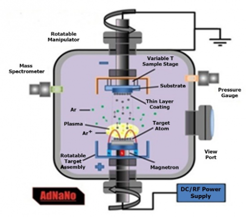
ITO thin films were fabricated using a PK 75 DC sputtering system equipped with a Trivac D 665 B rotary pump and a Turbotronic 1000/1500 rotary pump, as illustrated in Figure 1. The samples were analyzed by X-ray diffraction (XRD) and UV-Vis-NIR spectroscopy, Hall Effect measurements, and four-point probe testing. The sputtering system shown in Figure 1 consists of a chamber where the reaction takes place, which is equipped with a vacuum pump used to evacuate the chamber space. The vacuum system employs a Univex 450 model combined with a PK-75 sputtering cathode and a DCS-55S power supply. The vacuum is generated by a combination of a Trivac D 655 B rotary pump and a turbomolecular pump model Turbovae, capable of pumping at a rate of 1000 liters per second. Gas pressure within the vacuum is measured using a Combivac IT 230, while gas flow is regulated by a Master Flow mass flow controller type MKS 1359 C. Oxygen gas pressure control is performed using a Combivac CM 31. Substrate heating is provided by a radiant heater, and the temperature is monitored by a PT 100 resistance thermometer with a digital temperature controller (LH). The sputtering bath disk has a diameter of 19 cm and can accommodate eight substrates, each measuring 2.5 cm×7.5 cm×0.2 cm.
The deposition was performed by optimizing the oxygen partial pressure percentage and post-deposition annealing. The deposition was carried out in a vacuum chamber at a pressure of 10-5 mBarr. The sputtering process was initiated while argon and oxygen gases were simultaneously introduced through flow meters until the pressure reached 2×10-³ mBarr. The oxygen partial pressure introduced during each deposition was defined as the ratio of oxygen gas pressure to the total gas pressure, with values of 2.50%, 3.70%, 5.10%, 6.15%, and 8,9% for each sample. Annealing was conducted in a vacuum chamber at a pressure of 10-³ mBarr for 60 minutes at temperatures of 175℃ dan 250℃ for each sample.
The thickness of the thin films was calculated based on reflectance measurements obtained from UV-Vis spectroscopy within the wavelength range of 350-800 nm [13]. Microstructural analysis was performed using a Philips PW 3710 X-ray diffractometer equipped with a Co anode tube. The diffraction angle (2θ) was scanned from 20° to 70°, and peak positions (in degrees) along with Full Width at Half Maximum (FWHM) values were identified as the primary indicators [14]. Crystallite size, lattice strain, grain size, and lattice constants were determined from the XRD data [15].
Figure 1. DC sputtering instrument
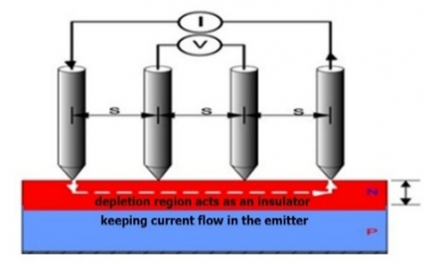
Electrical properties were analyzed using a four-point probe, as shown in Figure 2. Carrier concentration, charge carrier mobility, and band gap were determined using various equations. Optical properties of the ITO were measured using UV-Vis spectroscopy, with reflectance, transmittance, extinction coefficient, and absorption calculated from the UV-Vis data using specific equations.
Figure 2. Four-point probe instrument
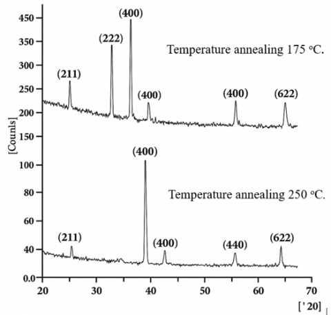
Electrical properties were measured using a four-point probe system Figure 2 manufactured by TOA digital super microammeter, model DSM 515 A. XRD measurements were performed using a Philips PW 3710 diffractometer with a cobalt anode. From the XRD measurements and analysis, the microcrystalline structure of ITO was characterized by X-ray diffraction, particularly in terms of grain size, lattice constants, and crystal orientation. The crystals obtained exhibited an (400) hkl plane orientation, as shown in Figure 3. Grain size (G) and lattice constants were calculated at the maximum orientation angle of 2θ, approximately 40.9°.
Figure 3. X-ray diffraction patterns of ITO films for different oxygen partial pressures
The XRD measurement patterns obtained from the ITO thin films exhibited a crystalline nature, with a tendency to show (400) orientation [16]. The coating plate orientation in the diffraction patterns was found to be consistent across all variations of oxygen content, indicating significant compatibility with the cubic bulk structure of In₂O₃. The highest intensity was observed at a diffraction angle (2θ) of 40.9°, corresponding to the (400) reflection of the body-centered cubic (bcc) structure. The intensities of the (400) and (222) reflections were prominent relative to the background intensity, indicating that the material structure had crystallized, as evidenced by the smaller FWHM. It is believed that this diffraction pattern shape resulted from the annealing temperature, which induced a transition of the material from the amorphous region [17].
The XRD patterns indicate that the maximum intensity occurs at the (400) plane, with a tendency to increase alongside the oxygen content. The increase in diffraction pattern intensity and the reduction in FWHM are associated with an increased concentration of oxygen vacancies and the diffusion rate resulting from annealing in the deposited layers. These changes are attributed to the reduction of free indium (In) atoms and tin (Sn) impurities due to oxidation by the oxygen introduced during deposition. Oxygen from the In₂O₃ and SnO₂ compounds is initially deposited because the boiling point of oxygen is lower than that of In and Sn, leading to oxygen deficiency.
The diffraction pattern intensity was observed to increase, while the FWHM decreased in samples annealed at 250℃, resulting in enhanced peak intensity and peak narrowing [18]. The peak with maximum intensity was obtained at the (222) plane, with a coating orientation of (400) at a deposition temperature of 150℃ using the electron beam method. Furthermore, it has been reported that amorphous indium oxide generally crystallizes rapidly at 150℃ with HDPE on the (222) plane.
In general, peak broadening in the X-ray diffraction patterns of crystalline samples is influenced by crystallite size and microstrain effects [19]. The diffraction peak broadening is assumed to be caused by small crystallite size rather than lattice strain [20].
Crystallite size was calculated from the XRD patterns using the Debye-Scherrer formula [21].
$G=\frac{0.9 \lambda}{\beta \cos \theta}$ (1)
where, λ is the X-ray wavelength, β is the FWHM in radians, and θ is the Bragg angle.
This equation states that the grain size depends on the ratio of the wavelength to the peak width and the diffraction angle, with an efficiency factor of 0.9. A narrow peak width (small β) at a larger wavelength (λ) will increase the grain size, provided that the measurement is taken near the principal direction (θ) approaching 0°.
The crystallite size formed was analyzed using Eq. (1), which describes the relationship between grain size (G) and other physical parameters. Grain size represents the strengthening effect produced in a specific direction compared to isotropic behavior. A higher G value indicates a more oriented and efficient direction in optical properties, particularly in transmittance and absorption. The parameter β represents the beamwidth. As the beamwidth narrows and grain size increases, the crystallinity of the formed crystals in the layer improves. The elevation angle factor (θ) indicates a decrease in grain size as the elevation angle moves away from the principal axis. Maximum grain size occurs at θ=0°, corresponding to the perpendicular direction.
Changes in grain size were associated with the level of oxygen vacancies and the diffusion rate resulting from the annealing temperature. The entire layer was perfectly crystallized into fine grains with sizes ranging from 68.99 to 122.76 nm. The average grain size increased to 112.09 nm at an annealing temperature of 175℃ and to 117.06nm at 250℃. The change in grain size between 175℃ and 250℃ was not significant due to most free atoms having already undergone diffusion.
The results obtained indicate that amorphous indium oxide generally crystallizes rapidly at 150℃. During the crystallization process, the entire layer becomes filled with grains that are nearly perpendicular to the surface [22]. The annealing temperature allows the crystals to grow larger and reach the surface, eventually contacting each other on the surface and eliminating amorphous regions.
The grain size was found to be comparable to that reported by Sobri et al. [23], Values ranging from 100 to 460 nm were observed at temperatures between 423 and 473 K, and grain sizes of 35 to 50 nm were obtained at 350℃ with 5% Sn. The lattice constant was determined to be 11.9nm at a substrate temperature of 600℃ [24].
The conversion of the lattice constant can be analyzed using the Cohen method [25].
$\frac{\Delta d}{d}=\frac{\Delta a}{a}=K \cos \theta$ (2)
$d_{h k l}=\frac{a}{\sqrt{h^2+k^2+l^2}}$ (3)
where, the lattice size is denoted as a, the lattice constant is represented by K, which is a constant equal to 0.9, and hkl indicates the preferred crystal orientation formed. Δd represents the change in the parameter d, which is the interplanar spacing between crystal planes, Δa represents the change in the parameter a, which is the spacing between the formed crystal lattice points, and K denotes the lattice constant of the formed crystal. The smallest lattice constant of 10.17 Å was observed at an oxygen partial pressure of 6.15% and annealing at 175℃. Lattice analysis results indicated lattice distortion, including contraction and expansion, due to the influence of oxygen partial pressure and annealing temperature. The lattice constant of the sample was found to be comparable to the ITO value from the ASTM card, which is 10.118 Å. The contraction of the lattice parameter obtained was considered acceptable due to its relatively small range, approximately between 0.052 and 0.212 Å.
The crystal lattice constant was observed to exhibit a decreasing trend with increasing oxygen partial pressure [26]. This change is attributed to distortions occurring in the crystal due to point defects caused by oxygen atoms, which are relatively small compared to the radii of In and Sn atoms, approximately 1.509 Å [27]. This local distortion acts as an additional scattering center for the electron current flowing through the crystal, resulting in increased resistance.
The lattice structure is altered due to strain, which is influenced by the contribution of oxygen vacancies. The effect of oxygen partial pressure during deposition is significant, with consistent changes observed in the lattice, while the lattice constant decreases with increasing annealing temperature due to a reduced Sn/In ratio [28]. The decrease in the lattice constant is attributed to the effects of microstrain and elastic strain caused by impurities and vacancies. The results of the thin film ITO structural analysis are presented in Table 1.
Table 1. Structural parameters of ITO thin films prepared under different oxygen partial pressures and annealing conditions
|
Oxygen Partial Pressure (%) |
Annealing Temperature (℃) |
20 (Degree) |
Intensity (Max) |
FWHM (Degree) |
HKL |
Lattice Constant (Å) |
Grain Size (hkl) (nm) |
|
2.50 |
175 |
41.065 |
400 |
0.16 |
400 |
10.25 |
122.81 |
|
250 |
40.955 |
729 |
0.16 |
400 |
10.23 |
122.76 |
|
|
3.70 |
175 |
40.880 |
745 |
0.18 |
400 |
10.24 |
109.44 |
|
250 |
41.250 |
686 |
0.16 |
400 |
10.21 |
122.80 |
|
|
5.10 |
175 |
41.060 |
729 |
0.18 |
400 |
10.21 |
109.51 |
|
250 |
40.910 |
226 |
0.18 |
400 |
10.21 |
109.10 |
|
|
6.15 |
175 |
41.180 |
325 |
0.18 |
400 |
10.17 |
109.55 |
|
250 |
35.345 |
350 |
0.16 |
222 |
10.19 |
120.70 |
|
|
8.90 |
175 |
41.060 |
747 |
0.18 |
400 |
10.20 |
109.16 |
|
250 |
41.135 |
1102 |
0.18 |
400 |
10.21 |
109.95 |
2.1 Electrical properties
ITO is a compound in which Sn is used as a dopant. The Sn atoms can be incorporated either by substituting one of the atoms in the primary In₂O₃ crystal or by occupying interstitial sites. Bonds with oxygen, such as SnO or SnO₂, can also be formed by Sn atoms, depending on their valence states of +2 or +4. The Sn⁴⁺ state in SnO₂ is known to act as an n-type donor, with electrons being released into the conduction band. The stabilization of the valence state of Sn depends on the synthesis conditions, where Sn⁴⁺ in SnO₂ is involved as an n-type electron donor through the release of electrons into the conduction band of In₂O₃ [29].
An increase in the concentration of Sn atoms in In₂O₃ induces the overlap of electron wave functions at the donor level (Sn⁴⁺), thereby modifying the periodic potential of the crystal lattice [30]. The occurrence of this overlap effect causes changes in the energy level potential of each electron, resulting in the formation of an energy band in the region. The impurity energy band will broaden and merge into the intrinsic band as the impurity concentration continues to increase.
The band tailing effect is caused by the disruption of lattice periodicity by dopant atoms, which leads to increased electron scattering and reduced mobility [31]. This impedance causes the lower energy band to expand, resulting in the narrowing of the energy band (band tailing effect).
The estimated critical donor density can be determined using the Mott criterion, where is the static dielectric constant of the host lattice (the effective mass in the conduction band is considered with the Bohr radius). $n_c^{\frac{1}{3}} a_0^* \approx 0.25 a_0^*=$ $\left.\frac{h^2 \varepsilon_0 \varepsilon^M}{\pi e^2 m_c^*} \varepsilon^M \varepsilon^M=\varepsilon^{l n_2 O_3}(\bar{\omega}=0)=8.9\right) .\left(m_c^*=0.35 m_e\right) a_0^* \approx$ $1.33 \mathrm{~nm}$. This value is consistent with experimental observations of the electron transport transition from doping mechanisms to band conduction [32].
The energy band structure of ITO with high doping density is presented.
$\begin{aligned} & E_c(k)=E_c^0+\hbar \Sigma_c(k) \\ & E_v(k)=E_v^0+\hbar \Sigma_v(k)\end{aligned}$ (4)
$E_v(k)$ represents the valence band energy with doping, and $E_c(k)$ represents the conduction band energy with doping.
Eq. (4) holds physical significance within the context of solid-state physics, particularly in the theory of electronic energy bands. $E_c(k)$ represents the conduction band energy at the wave vector k . corresponding to the energy possessed by an electron in the conduction band for a given momentum. $E_c^0$ denotes the conduction band energy without considering interaction effects, while $\Sigma_c(k)$ is the self-energy function representing energy corrections due to electron interactions with the surrounding environment, such as electron-electron and electron-phonon interactions, at conduction band and momentum $k$. This equation expresses that the actual electron energy in the conduction band $E_v(k)$ is the sum of the base conduction band energy $E_c^0$ and the energy correction $\hbar \Sigma_c(k)$. arising from interactions. These corrections cause shifts and changes in the bandwidth from their ideal values.
The density and mobility of charge carriers in extrinsic semiconductors are influenced by the availability of free electrons.
$\mu=\left(\frac{4 e}{h}\right)\left(\frac{\pi}{3}\right)^{1 / 3} n^{-2 / 3}$ (5)
μ represents the carrier mobility, and n represents the electron density. The electrical conductivity, σ, can be expressed by the equation. This equation is used to estimate the mobility in crystals where electron-electron interactions and other effects can be neglected. The equation demonstrates the theoretical relationship between electron mobility and electron concentration within the free electron gas model. Mobility is decreased as the carrier concentration increases, which is important for understanding the electrical transport properties of crystalline materials.
$\sigma=e\left(\mu_n+\mu_h p\right) \frac{1}{\rho}$ (6)
σ represents the electrical conductivity, and ρ represents the electrical resistivity.
The total conductivity in crystals formed in thin films is given by the sum of the contributions from electrons and holes, each multiplied by their respective charge and mobility.
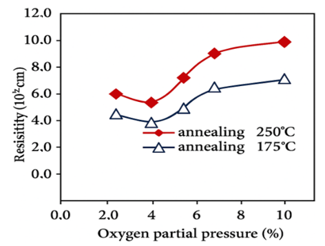
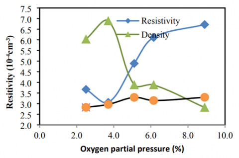
The resistivity of the thin films as a function of oxygen partial pressure and annealing is shown in Figure 4. The lowest resistivity of the ITO thin films was obtained at an oxygen partial pressure of 3.7% with annealing treatment at 250℃. This resistivity is associated with a carrier density of 6.89×10²⁰ cm⁻³, a carrier mobility of 29.64 cm²/V·s, and a band gap of 3.92 eV.
ITO thin films fabricated at the same oxygen partial pressure but subjected to different annealing treatments exhibit varying resistivities. Meanwhile, the resistivity of the ITO thin film prepared at an oxygen partial pressure of 3.7% and annealed at 175℃ was found to be higher than that of the thin film annealed at 250℃.
Based on the analysis of Figure 4, it can be concluded that a clear relationship exists between oxygen partial pressure and electrical resistivity in thin films. The material’s resistivity, which represents the ability of a material to inhibit electric current flow, was found to be significantly dependent on variations in oxygen partial pressure and annealing parameters.
Figure 4. Resistivity as a function of oxygen partial pressure and annealing
Under low oxygen pressure conditions, an increase in oxygen vacancies, which act as electron donors, was observed to cause a decrease in resistivity. Conversely, at high oxygen partial pressures, a reduction in oxygen vacancy concentration was noted, leading to a decrease in charge carriers and consequently an increase in resistivity.
The annealing process was shown to exert additional influence on resistivity through mechanisms involving the filling or formation of oxygen vacancies. Annealing in oxygen-rich environments was observed to fill existing vacancies, while annealing at elevated temperatures under oxygen-deficient conditions was found to promote the formation of new vacancies, thereby enhancing conductivity.
The observed effects are related to the crystallinity level. This is evidenced by the lower carrier density obtained, which is 4.86×10²⁰ cm⁻³, and a mobility of 34.02 cm²/V·s.
Changes in carrier density and mobility are attributed to the contribution of free electrons to ITO, originating from the diffusion of Sn⁴⁺ dopant atoms substituting Sn³⁺ atoms in the host In₂O₃ lattice, as described by Eq. (4). The electron contribution from Sn, due to its bonding with oxygen and substitution for in atoms in the In₂O₃ lattice, is correlated with the carrier density, which leads to changes in electrical resistivity. These changes are also caused by free electrons from In and Sn atoms that cannot be oxidized due to an increased concentration of oxygen vacancies during deposition. During annealing, the In₂O₃ compound releases some oxygen, resulting in a non-stoichiometric composition initially represented as In2O3-x (Vo")xe2x, where Vo" denotes oxygen vacancies with two electrons and e2x' denotes electrons required to neutralize the vacancies. Similarly, SnO₂ releases some oxygen, producing a composition initially represented as SnO2-x (Vo")x $e_{2 x}{ }^{\prime}$. Generally, the thin film samples are estimated to have the formula, $I n_{2-y} S n_y^{\prime O_{3-x}}\left(V_0^{\prime \prime}\right)_x e_{2 x}^{\prime e_{y^{\prime}} S n_{y^{\prime}}}$, with Sn substituting for In, resulting in one free electron per substitution.
Oxidation conditions result in changes in the concentration of oxygen vacancies, which in turn can cause variations in carrier density. An increase in oxygen content in the ITO layer can also enhance the orientation of carrier mobility. On the other hand, oxygen content may induce changes in carrier density without causing significant alterations in carrier mobility. The effect of increased oxygen density at insertion sites within grain boundaries and oxides was not observed.
Table 2 presents the characterization of electrical and optical properties of indium tin oxide (ITO) thin films deposited under varying oxygen partial pressures and annealed at two distinct temperatures 175℃ and 250℃. Key parameters evaluated include resistivity 10⁻⁴ Ω cm, charge carrier concentration 10²⁰ cm⁻³, mobility and optical bandgap.
Table 2. Electrical parameters of ITO thin films prepared under different oxygen partial pressures and annealing conditions
|
Oxygen Partial Pressure (%) |
Annaeling (℃) |
Resistivity ($\times10^{-4}\mathrm{~cm}^{-3}$ ) |
Carrier Concentration (n) ($\times\mathbf{10}^{\mathbf{2 0}}\mathbf{c m}^{-\mathbf{3}}$) |
Mobility (μ) ($\mathrm{cm}^2 V^{-1} s^{-1}$) |
Band Gap (eV) |
|
2.50 |
175 |
5.50 |
5.39 |
21.49 |
3.92 |
|
250 |
3.67 |
6.03 |
28.24 |
3.81 |
|
|
3.70 |
175 |
4.89 |
6.51 |
19.63 |
4.29 |
|
250 |
3.06 |
6.89 |
29.64 |
3.92 |
|
|
5.10 |
175 |
7.34 |
3.38 |
25.19 |
4.20 |
|
250 |
4.89 |
3.88 |
32.94 |
3.78 |
|
|
6.15 |
175 |
9.17 |
3.05 |
22.35 |
4.30 |
|
250 |
6.11 |
3.25 |
31.47 |
4.10 |
|
|
8.90 |
175 |
9.78 |
2.77 |
22.86 |
4.35 |
|
250 |
6.72 |
2.82 |
32.98 |
4.20 |
At lower pO2 levels 2.5%-3.7%, lower resistivity was observed in the films 3.67×10⁻⁴ Ω cm at 2.5% pO2, 250℃ annealing, attributed to increased oxygen vacancies acting as electron donors, which elevated charge carrier concentration (n). However, this condition was also associated with slightly reduced mobility (μ) and a narrower optical bandgap 3.81 eV at 2.5% pO2, 250℃ annealing due to the Burstein-Moss effect. In contrast, higher pO2 levels 5.1%-8.9% resulted in increased resistivity 9.78×10⁻⁴ Ω cm at 8.9% pO2, 175℃ annealing, caused by diminished oxygen vacancies that reduced charge carrier density. Nevertheless, mobility was significantly enhanced 32.98 cm²/Vs at 8.9% pO2, 250℃ annealing owing to fewer defects, while the optical bandgap widened 4.35 eV at 8.9% pO2, 175℃ annealing, improving optical transparency.
Superior electrical performance was consistently obtained with 250℃ annealing compared to 175℃. For instance, at 2.5% pO2, resistivity decreased from 5.50×10⁻⁴ Ωcm to 3.67×10⁻⁴ Ωcm, carrier concentration increased from 5.39×10²⁰ cm⁻³ to 6.03×10²⁰ cm⁻³, and mobility improved from 21.49 cm²/Vs to 28.24 cm²/Vs. These trends were attributed to enhanced crystallinity and defect passivation at higher annealing temperatures. An optimal balance between low resistivity and high mobility was achieved at 3.7% pO2 with 250℃ annealing, resistivity 3.06×10⁻⁴ Ωcm; mobility 29.64 cm²/V s.
Changes in carrier density and mobility are caused by several processes during annealing, including oxygen absorption and diffusion within the thin film. Oxygen diffusion can lead to a reduction in oxygen vacancies. During annealing, dopant Sn atoms are diffused from grain boundaries and interstitial lattice sites to normal lattice sites, enabling Sn to act as an active donor due to its higher atomic valence compared to In. This annealing process enhances crystallinity or crystal growth, thereby minimizing scattering at grain boundaries.
The change in electrical resistivity of ITO layers after annealing is caused by opposing processes of oxygen absorption and Sn diffusion. Oxygen diffusion causes oxygen atoms to be absorbed into the ITO thin film, resulting in a reduction of oxygen vacancies during the annealing process. Conversely, Sn diffusion involves the movement of Sn atoms from grain boundaries and interstitial sites to In₂O₃ lattice sites, forming SnO₂ oxide. In general, Sn donors are activated upon reaching specific temperatures, leading to a significant increase in free electron density within the ITO thin films, as demonstrated in Figure 5.
Figure 5. Resistivity, carrier density, and mobility at an annealing temperature of 250℃
The decrease in the density of ITO material by 3.7% at an oxygen partial pressure (pO₂) of 3.70% is associated with the formation of suboxide compounds such as InO and SnO, as well as free In and Sn atoms that act as ionic scattering centers [33]. An increase in the concentration of in° (0.8%) and Sn° (1.2%) under these conditions was detected through X-ray photoelectron spectroscopy (XPS) analysis, revealing a reduction in the periodicity of the crystal lattice and an increase in interfacial defects [34].
The minimum resistivity (3.06×10⁻⁴ Ω·cm) was achieved at a pO₂ 3.70% due to the optimization of oxygen vacancy concentration (V₀) at approximately ~2.1×10²⁰ cm⁻³, resulting in an increase in carrier density (n) to 9.5×10²⁰ cm⁻³. However, an increase in pO₂ to 8.90% caused excessive oxidation with the formation of secondary SnO₂ and a reduction of (V₀) to 1.3×10²⁰ cm⁻³, which led to an increase in resistivity to 6.72×10⁻⁴ Ω·cm [35].
The annealing process at 250℃ was utilized to facilitate grain recrystallization, during which the electron mobility (μ) was increased from 18.7 cm²/V·s to 24.5 cm²/V·s through the reduction of grain boundary scattering [36]. This effect was limited to pO₂≤3.70% because external oxygen diffusion led to the filling of oxygen vacancies (V₀) and the suppression of charge carrier generation.
Reflectance (R) is defined as the ratio of the reflected energy flux to the incident energy flux.
$R=\frac{\left(n_2-1\right)^2+k^2}{\left(n_2+1\right)^2+k^2}$ (7)
Reflectance R, defined as the fraction of light intensity reflected when light is incident from air, depends on the real refractive index n2 of the material and the extinction coefficient k which is the imaginary part of the complex refractive index describing the material’s light absorption strength. Eq. (7) is used to calculate the surface reflectivity of thin-film optics. This equation indicates how much light is reflected from the surface of a material based on its optical properties, specifically the real refractive index n2 and extinction coefficient k.
Transmission (T) of thin films can be determined by:
$T=\left|\frac{2 n_1}{n_2+n_1}\right|$ (8)
Transmittance T indicates the extent to which the amplitude of a wave successfully penetrates the boundary between two media. When n₁ and n₂ differ significantly, most of the wave is reflected, and only a small portion is transmitted, meaning that the entire wave is transmitted without reflection. This equation describes the efficiency of amplitude transmission of light at the boundary between two media with different refractive indices and is highly important in the design and analysis of optical systems.
The relationship between the absorption coefficient (α) and the extinction coefficient (k) can be expressed by:
$\alpha=\frac{4 \pi k}{\lambda}$ (9)
This equation has a physical meaning as the absorption coefficient α in optics. The absorption coefficient represents the rate of light absorption by the material at a specific wavelength. The extinction coefficient k, which is the imaginary part of the material's complex refractive index, indicates the level of light absorption by the material.
The absorption coefficient (α), extinction coefficient (k), and wavelength (λ) are related, and the transmission of electrons undergoing direct transitions can be mathematically described.
$\alpha\ h\ v \approx\left(h\ v-E_q\right)^n$ (10)
With Eg representing the energy band gap of the transition, photon energy, and n=1/2 for direct transitions and n=3/2 for indirect transitions.
This equation indicates that a quantitative relationship exists between the available energy $(h\ v)$ and the energy required for the transition $\left(E_g\right)$. When the available energy $(h\ v)$ exceeds the energy gap $\left(E_g\right)$, energy transitions can occur, and vice versa. This equation is used to understand the phenomena of light absorption, photon emission, and electron transitions in atoms, as well as how the energy gap influences energy transitions.
Table 3 presents the characterization of the optical properties of indium tin oxide (ITO) thin films deposited under varying oxygen partial pressures (pO₂) and subjected to annealing at two distinct temperatures (175℃ and 250℃). The measured parameters include reflectance (%), refractive index, extinction coefficient (k), absorption coefficient (α), and maximum transmittance (%). These deposition conditions were found to significantly influence the optical performance of the ITO films.
Table 3. Optical parameters of ITO thin films for different oxygen partial pressures and annealing conditions
|
Oxygen Partial Pressure (%) |
Annaeling (℃) |
Wave Lenght (nm) |
Ref (%) |
Refractive Index |
Extinction Coefficient (K) |
Absorpsi ($\alpha$ ) |
Maximum Transmission (%) |
|
2.50 |
175 |
686 |
11.96 |
2.18 |
3.30 |
0.061 |
81.94 |
|
250 |
598 |
10.38 |
2.20 |
3.34 |
0.070 |
82.65 |
|
|
3.70 |
175 |
664 |
9.65 |
2.20 |
3.36 |
0.063 |
84.05 |
|
250 |
615 |
8.39 |
2.18 |
3.36 |
0.069 |
84.71 |
|
|
5.10 |
175 |
591 |
8.40 |
2.20 |
3.38 |
0.072 |
84.41 |
|
250 |
615 |
7.70 |
2.20 |
3.40 |
0.072 |
85.05 |
|
|
6.15 |
175 |
727 |
9.61 |
2.09 |
3.08 |
0.053 |
85.07 |
|
250 |
664 |
10.76 |
2.22 |
1.93 |
0.036 |
85.59 |
|
|
8.90 |
175 |
668 |
7.00 |
2.22 |
3.44 |
0.065 |
86.60 |
|
250 |
700 |
6.61 |
2.25 |
3.49 |
0.062 |
87.12 |
Critical trends were identified from the data. An increase in oxygen partial pressure from 2.5% to 8.9% was observed to induce changes in optical transmittance, with maximum transmittance values rising from 81.94% to 87.12% at the highest pO₂ and annealing temperature. This enhancement in transparency correlated with reduced reflectance, particularly at higher pO₂ levels, where reflectance decreased from 11.96% to 6.61%. The refractive index remained relatively stable across all conditions (2.18-2.25), indicating consistent film density, while the extinction coefficient exhibited greater variability, ranging from 1.93 to 3.49. The absorption coefficient maintained low values (0.03-0.07), reflecting favorable optical quality. Annealing at 250℃ consistently produced superior optical performance compared to 175℃ under identical pO₂ conditions, as evidenced by higher transmittance percentages and lower reflectance values.
These results demonstrate that both oxygen partial pressure during deposition and post-deposition annealing temperature critically influence the optical characteristics of ITO films. The optimal combination was identified as 8.9% pO₂ with 250℃ annealing, achieving the highest transmittance (87.12%) and lowest reflectance (6.61%). The data confirm that precise control of oxygen partial pressure during deposition and annealing temperature can effectively modulate the optical properties of ITO films.
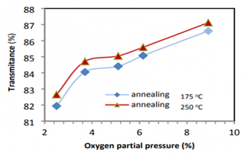
Transmission is altered by partial oxygen pressure and annealing level, as shown in Figure 6.
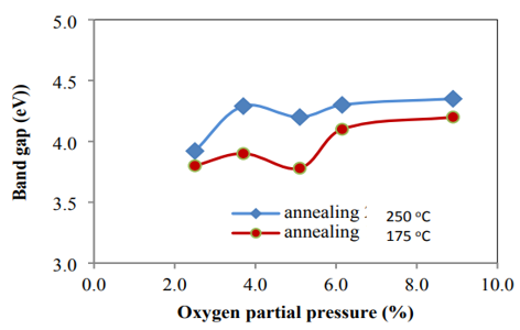
Figure 6. Band gap energy of ITO
Changes in the energy band gap of the ITO coating are influenced by variations in partial oxygen pressure and annealing, as shown in Figure 5. The band gap changes because the concentration of Sn doping atoms begins to decrease due to the bonding of Sn atoms with oxygen introduced from the outside. Consequently, the electron wave functions at the impurity levels no longer overlap, affecting the changes in the potential energy levels of each electron, which may lead to the formation of an energy band in that region. Another effect arising from the reduced impurity concentration is the expansion of the lower energy band, causing the band gap energy to experience a band tailing effect.
Figure 7. Transmission ITO
The shift in the energy band gap can also be associated with the annealing temperature, which is related to the diffusion rate of oxygen atoms at the grain boundaries. An increase in partial oxygen pressure can cause an increase in transmission, as shown in Figure 7, due to changes in the crystallization of the ITO thin film, with the FWHM increasing as indicated in Figure 3. The ITO-coated grains begin to transition from an amorphous structure to fine grains with sizes ranging from 68.99 nm to 122.76 nm at temperatures between 150℃ and 250℃.
Changes in the transmission pattern of the ITO layer in response to partial oxygen pressure and annealing variations are shown in Figure 7. The high transmission observed in several samples up to a certain range appears to correspond to the properties of the ITO material, which has a wide band gap ranging from 3.78 eV to 4.35 eV.
The band gap shift due to vacancies is formulated by Burstein-Moss [37].
$E_g^{f f}=E_{g 0}+\Delta \Sigma_g^{B M}+\hbar \Sigma(k)$ (11)
where, the contribution of electron scattering is caused by impurities. To reduce the contribution of electron impurities from In and Sn, the addition of partial oxygen pressure causes a decrease in electron impurities, resulting in an increase in the energy band gap [38]. This equation indicates that the energy gap does not depend solely on the intrinsic value $\left(E_{g 0}\right)$, but is also influenced by many-body interactions and quantum effects related to the electronic states within the material. The interaction functions $\Delta \Sigma_g^{B M}$ dan $\hbar \Sigma(k)$ which represent electron-electron interactions and quantum effects, can affect the electrical and optical properties of the material.
Optimization of ITO thin films as transparent conductors was conducted using the sputtering technique, focusing on the effects of variations in partial oxygen pressure and annealing temperature on the electrical and optical characteristics. The crystal structure of the thin films, dominated by the (400) plane orientation, was shown to depend on the partial oxygen pressure and thermal conditions. Changes in lattice constants and reductions in grain size were observed with increasing partial oxygen pressure, while high-temperature annealing treatment induced recrystallization that improved the structural order.
Significant resistivity reduction of up to 3.70% was found in ITO thin films when the partial oxygen pressure was optimized. Electrical conductivity was further enhanced by annealing treatment at 250℃ through the reduction of crystal defects and the increase of charge carrier mobility. Meanwhile, the optical properties of the ITO thin films were also influenced by these parameters. Optical transmission increased with rising partial oxygen pressure, reaching a maximum value of 87.12% at the optimal combination of partial oxygen pressure and annealing at 250℃. This phenomenon was attributed to the reduction of light scattering due to improved surface homogeneity and decreased optical defects.
These findings indicate that control of the partial oxygen pressure during deposition and manipulation of the annealing temperature are critical innovations in engineering the electrical and optical properties of ITO thin films. The combination of these two parameters not only influences the crystal structure but also opens opportunities for optimizing material performance for optoelectronic applications such as solar cells and transparent displays.
Systematic exploration of the combination of parameters within the partial oxygen pressure range (2-5%) and annealing temperature variation (200-300℃) can be performed to identify the optimal point that balances electrical properties (low resistivity) and optical properties (high transmission).
The interaction mechanism between oxygen partial pressure during deposition and annealing temperature dynamics needs to be further investigated, including its effects on crystal defect distribution, charge carrier concentration, and recrystallization processes.
Advanced characterization techniques such as high-resolution TEM or X-ray photoelectron spectroscopy (XPS) are recommended to be employed in order to map the relationships between oxygen pressure, grain size, surface composition, and oxygen defects that influence the electrical-optical performance.
|
β |
XRD peak half-width, degree |
|
Ɵ |
scattering angle, rad |
|
λ |
wave length, nm |
|
Å |
unit layer thickness |
|
α |
thin film absorption |
|
R |
reflectance, % |
|
T |
transmission, % |
|
m |
wavenumber |
|
n |
refractive index |
|
G |
grain size, nm |
|
h |
Planck constant |
|
k |
extinction coefficient |
|
μ |
charge carrier mobility |
|
σ |
electrical conductivity |
|
ρ |
electrical resistivity |
|
Subscripts |
|
|
ITO |
indium tin oxide |
|
UV-Vis |
ultra violet visible |
|
XRD |
X-ray diffraction |
[1] Ma, Z., Li, Z., Movahhed Nouri, B., Liu, K., Ye, C., Dalir, H., Sorger, V.J. (2023). Indium-Tin-Oxide for high-performance electro-optic modulation. arXiv. https://doi.org/10.48550/arXiv.2305.10639
[2] Marangi, F., Fenzi, L., Bellingeri, M., Scotognella, F. (2023). Role of the annealing parameters on the resistance of indium tin oxide nanocrystalline films. Optical Materials, 140: 113860. https://doi.org/10.1016/j.optmat.2023.113860
[3] Ahmed, M., Bakry, A., Qasem, A., Dalir, H. (2020). The main role of thermal annealing in controlling the structural and optical properties of ITO thin film layer. arXiv. https://arxiv.org/abs/2104.07464.
[4] Ji, Y.C., Zhang, H.X., Zhang, X.H., Li, Z.Q. (2013). Structures, optical properties, and electrical transport processes of SnO2 films with oxygen deficiencies. Physica Status Solidi (b), 250(10): 2145-2152. https://doi.org/10.1002/pssb.201349086
[5] Vilca-Huayhua, C.A., Mishra, S., Martinez, M.A.R., Guerra, J.A., Villegas-Lelovsky, L., Aragon, F.F.H. (2025). Tailoring structural, electrical, and optical properties of ITO thin films via vacuum-pressure annealing: An experimental and theoritical study. Journal of Alloys and Compounds, 1017: 178909. https://doi.org/10.1016/j.jallcom.2025.178909
[6] Nistor, M., Gherendi, F., Dobrin, D., Perrière, J. (2022). From transparent to black amorphous zinc oxide thin films through oxygen deficiency control. Journal of Applied Physics, 132(22). https://doi.org/10.1063/5.0129135
[7] Xiao, J., Zeng, G., Li, J., Zhang, S. (2023). The effect of the crystallization of indium tin oxide on indium tin oxide wet etching based on gate line with the structure of copper/indium tin oxide. Journal of The Society for Information Display, 31(8): 522-528. https://doi.org/10.1002/jsid.1216
[8] Chen, A., Zhu, K., Zhong, H., Shao, Q., Ge, G. (2014). A new investigation of oxygen flow influence on ITO thin films by magnetron sputtering. Solar Energy Materials and Solar Cells, 120: 157-162. https://doi.org/10.1016/j.solmat.2013.08.036
[9] Sharme, R.K., Quijada, M., Terrones, M., Rana, M.M. (2024). Thin conducting films: Preparation methods, optical and electrical properties, and emerging trends, challenges, and opportunities. Materials, 17(18): 4559. https://doi.org/10.3390/ma17184559
[10] Senthilkumar, V., Vickraman, P., Jayachandran, M., Sanjeeviraja, C. (2010). Structural and optical properties of indium tin oxide (ITO) thin films with different compositions prepared by electron beam evaporation. Vacuum, 84(6): 864-869. https://doi.org/10.1016/j.vacuum.2009.11.017
[11] Park, J.H., Buurma, C., Sivananthan, S., Kodama, R., Gao, W., Gessert, T.A. (2014). The effect of post-annealing on Indium Tin Oxide thin films by magnetron sputtering method. Applied Surface Science, 307: 388-392. https://doi.org/10.1016/j.apsusc.2014.04.042
[12] Tantray, F.A., Agrawal, A., Gupta, M., Andrews, J.T., Sen, P. (2016). Effect of oxygen partial pressure on the structural and optical properties of ion beam sputtered TiO2 thin films. Thin Solid Films, 619: 86-90. https://doi.org/10.1016/j.tsf.2016.10.020
[13] Abdullah, M.T., Raoof, L.M., Hasan, M.H., Abd, A.N., Mohammed, I.M. (2021). The effect of different thickness on the optical and electrical properties of TiO2 thin films. Journal of Physics: Conference Series, 1999(1): 012128. https://doi.org/10.1088/1742-6596/1999/1/012128
[14] Fatimah, S., Ragadhita, R., Al Husaeni, D.F., Nandiyanto, A.B.D. (2022). How to calculate crystallite size from x-ray diffraction (XRD) using Scherrer method. ASEAN Journal of Science and Engineering, 2(1): 65-76. https://doi.org/10.17509/ajse.v2i1.37647
[15] He, K., Chen, N., Wang, C., Wei, L., Chen, J. (2018). Method for determining crystal grain size by x‐ray diffraction. Crystal Research and Technology, 53(2): 1700157. https://doi.org/10.1002/crat.201700157
[16] Hossain, M.I., Salhi, A., Zekri, A., Abutaha, A., Tong, Y., Mansour, S. (2025). Studying room temperature RF magnetron-sputtered indium tin oxide (ITO) thin films for large scale applications. Results in Surfaces and Interfaces, 18: 100383. https://doi.org/10.1016/j.rsurfi.2024.100383
[17] Sethi, G., Bontempo, B., Furman, E., Horn, M.W., Lanagan, M.T., Bharadwaja, S.S.N., Li, J. (2011). Impedance analysis of amorphous and polycrystalline tantalum oxide sputtered films. Journal of Materials Research, 26(6): 745-753. https://doi.org/10.1557/jmr.2010.77
[18] Vashista, M., Paul, S. (2012). Correlation between full width at half maximum (FWHM) of XRD peak with residual stress on ground surfaces. Philosophical Magazine, 92(33): 4194-4204. https://doi.org/10.1080/14786435.2012.704429
[19] Disha, S.A., Hossain, M.S., Habib, M.L., Ahmed, S. (2024). Calculation of crystallite sizes of pure and metals doped hydroxyapatite engaging Scherrer method, Halder-Wagner method, Williamson-Hall model, and size-strain plot. Results in Materials, 21: 100496. https://doi.org/10.1016/j.rinma.2023.100496
[20] Zhang, X., Zhang, G., Yan, Y. (2023). Effects of doping ratio and thickness of indium tin oxide thin films prepared by magnetron sputtering at room temperature. Coatings, 13(12): 2016. https://doi.org/10.3390/coatings13122016
[21] Sundaram, P.S., Sangeetha, T., Rajakarthihan, S., Vijayalaksmi, R., Elangovan, A., Arivazhagan, G. (2020). XRD structural studies on cobalt doped zinc oxide nanoparticles synthesized by coprecipitation method: Williamson-Hall and size-strain plot approaches. Physica B: Condensed Matter, 595: 412342. https://doi.org/10.1016/j.physb.2020.412342
[22] Li, J., Jiang, L., Li, X., Luo, J., Liu, J., Wang, M., Yan, Y. (2023). Different crystallization behavior of amorphous ITO film by rapid infrared annealing and conventional furnace annealing technology. Materials, 16(10): 3803. https://doi.org/10.3390/ma16103803
[23] Sobri, M., Shuhaimi, A., Hakim, K.M., Ganesh, V., Mamat, M. H., Mazwan, M., Najwa, S., Ameera, N., Yusnizam, Y., Rusop, M. (2014). Effect of annealing on structural, optical, and electrical properties of nickel (Ni)/indium tin oxide (ITO) nanostructures prepared by RF magnetron sputtering. Superlattices and Microstructures, 70: 82-90. https://doi.org/10.1016/j.spmi.2014.02.010
[24] Chauhan, R.N., Tiwari, N. (2021). Preparation of optically transparent and conducting radio-frequency sputtered indium tin oxide ultrathin films. Thin Solid Films, 717: 138471. https://doi.org/10.1016/j.tsf.2020.138471
[25] Han, S., Hu, C., Yu, J., Jiang, H., Wen, S. (2021). Stabilization of inertial Cohen-Grossberg neural networks with generalized delays: A direct analysis approach. Chaos, Solitons & Fractals, 142: 110432. https://doi.org/10.1016/j.chaos.2020.110432
[26] Hoshina, T., Sase, R., Nishiyama, J., Takeda, H., Tsurumi, T. (2018). Effect of oxygen vacancies on intrinsic dielectric permittivity of strontium titanate ceramics. Journal of the Ceramic Society of Japan, 126(5): 263-268. http://doi.org/10.2109/jcersj2.17250
[27] Ali, A., Zhang, J.M., Muhammad, I., Shahid, I., Ahmad, I. (2020). Modulating the electronic, magnetic and optical properties of 1T-SnSe2 monolayer by defects: An ab initio study. Superlattices and Microstructures, 145: 106621. https://doi.org/10.1016/j.spmi.2020.106621
[28] Biswas, D., Sinha, A.K., Chakraborty, S. (2016). Effects of oxygen partial pressure and annealing temperature on the residual stress of hafnium oxide thin-films on silicon using synchrotron-based grazing incidence X-ray diffraction. Applied Surface Science, 384: 376-379. https://doi.org/10.1016/j.apsusc.2016.05.015
[29] Colvin, J., Ciechonski, R., Gustafsson, A., Samuelson, L., B. Ohlsson, J., Timm, R. (2020). Local deffect-enhances anodic oxidation of reformed GaN nanowires. Physical Review Materials, 4: 074603. https://doi.org/10.1103/PhysRevMaterials.4.074603
[30] Darabi, S., Yang, C.Y., Li, Z., Huang, J.D., Hummel, M., Sixta, H., Fabiano, S., Muller, C. (2023). Polymer-based n-type yarn for organic thermoelectric textiles. Advance Electronic Materials, 9(4): 2201235. https://doi.org/10.1002/aelm.202201235
[31] Liu, C., Hao, S., Chen, X., Zong, B., Mao, S. (2020). High anti-interfere Ti3C2Tx MXene field-effect-transistor-based-alkali indicator. Functional Inorganic Materials and Devices, 12(29): 38554-38563. https://doi.org/10.1021/acsami.0c09921
[32] Handa, T., Tahara, H., Aharen, T., Shimazaki, A., Wakamiya, A., Kanemitsu, Y. (2020). Large thermal expansion leads to negative thermo-optic coefficient of halide perovskite CH3NH3PbCL3. Physical Review Materials, 4(7): 074604. https://doi.org/10.1103/PhysRevMaterials.4.074604
[33] Qiao, H., Zhang, Y., Yan, Z.H., Duan, L., Ni, L., Fan, J.B. (2022). A type-II GaN/InS van der Waals heterostructure with high solar-to-hydrogen efficiency of photocatalyst for water splitting. Applied Surface Science, 604: 154602. https://doi.org/10.1016/j.apsusc.2022.154602
[34] Arnay, I., Serrano, A., Braza, V., Cid, R., Sánchez, A.M., Sánchez, J.L., Castro, G.R., Zuazo, J.R. (2023). Soft magnetism in single phase Fe3Si thin films deposited on SrTiO3(001) by pulsed laser deposition. Journal of Alloys and Compounds, 947: 169540. https://doi.org/10.1016/j.jallcom.2023.169540
[35] Sharma, P., Mehata, M.S. (2020). Rapid Sensing of lead metal ion in an aqueous medium by MoS2 quantum dots fluorescense turn-off. Materials Research Bulletin, 131: 110978. https://doi.org/10.1016/j.materresbull.2020.110978
[36] Espanol, M., Davis, E., Meslet, E., Mestress, G., Montufar, E.B., Ginebra, M.P. (2023). Effect of Moisture on the reactivity of alpha-tricalcium phospate. Ceramics International, 49(11): 18231-18239. https://doi.org/10.1016/j.ceramint.2023.02.193
[37] Khan, A., Rahman, F., Nongjai, R., Asokan, K. (2020). Structural, optical and electrical transport properties of Sn doped In2O3. Elsevier: Solid State Sciences, 109: 106436. https://doi.org/10.1016/j.solidstatesciences.2020.106436
[38] Dekkers, J.M., Rijnders, G., Blank, D.H. (2006). Role of Sn doping in In2O3 thin films on polymer substrates by pulsed-laser deposition at room temperature. Applied Physics Letters, 88(15): 151908. https://doi.org/10.1063/1.2195096