
Mohammad Tariq Yaseen | Shamil H. Hussein* | Falah Hasan Mohammed
© 2026 The authors. This article is published by IIETA and is licensed under the CC BY 4.0 license (http://creativecommons.org/licenses/by/4.0/).
OPEN ACCESS
This paper presents the design and performance enhancement of a broadband gallium nitride (GaN) based non-uniform distributed power amplifier (NDPA) employing a 10 W CGH60008D 0.4 µm gallium nitride on silicon carbide (GaN-on-SiC) high-electron-mobility transistor (HEMT) for ultra-wideband microwave applications. The proposed amplifier employs tapered gate and drain artificial transmission lines (ATLs) and a harmonic suppression network to mitigate parasitic effects, improve impedance matching and enhance broadband power-added efficiency (PAE). The amplifier design and analysis were based on the Advanced Design System (ADS) simulations with the Class-AB bias conditions of VDS = 28 V and VGS = −1.6 V. The obtained results showed a broadband operation over a 2–16 GHz frequency range with small-signal gain from 11.2 dB to 2.2 dB, saturated output power from 35 dBm to 39 dBm and a maximum PAE of 48%. Moreover, the proposed NDPA has demonstrated acceptable broadband impedance matching and stable large-signal performance across the operating band. The results obtained confirm that the combination of non-uniform distributed architecture and harmonic suppression techniques provides an effective trade-off between bandwidth, gain, output power and efficiency. The proposed amplifier is suitable for broadband communication systems.
non-uniform distributed power amplifier, gallium nitride high-electron-mobility transistor, high-efficiency, broadband amplifiers
The rapid growth of modern wireless communication systems, such as fifth-generation (5G), emerging sixth-generation (6G) networks, radar systems, and electronic warfare (EW) applications, has dramatically increased the need for broadband, high-efficiency, and high-power radio frequency (RF) power amplifiers (PAs). In these systems, the amplifiers need to work in ultra-wide bandwidths while still maintaining high output power and efficiency. In particular, wideband operation over multi-octave frequency ranges is essential for supporting spectrum aggregation, multi-standard communication and high-resolution sensing applications [1].
Gallium nitride (GaN) high-electron-mobility transistors (HEMTs) have become a key enabling technology for such high-performance PAs due to their superior material properties such as wide bandgap, high breakdown voltage, high current density and excellent thermal conductivity [2]. GaN devices have many advantages over traditional gallium arsenide (GaAs) technologies, such as higher power density and higher efficiency, and are very promising for broadband and high-power applications [3]. Thus, GaN-based monolithic microwave integrated circuit (MMIC) is the most attractive candidate for the next generation RF front-end systems [4].
Conventional wideband PA design techniques primarily depend on reactive matching networks for the impedance transformation over a desired frequency range [5]. Nevertheless, the performance of these techniques is intrinsically limited by the Bode-Fano criterion, limiting the achievable bandwidth for a given impedance match, especially under the high-voltage operating conditions of GaN devices. This makes it difficult to achieve wide bandwidth, high efficiency, and high output power using conventional matching-based topologies [6]. Alternatively, distributed amplifiers (DAs) have been extensively studied for broadband applications due to the use of artificial transmission lines (ATLs) at the gate and drain to absorb the transistor parasitic capacitances and thus extend bandwidth and alleviate high-frequency gain roll-off [7]. However, conventional DAs have several critical limitations, such as low power-added efficiency (PAE), power dissipation in termination resistors and non-uniform signal distribution over the transistor cells that degrade the performance and limit the applicability of DAs for high-efficiency broadband systems [8].
To overcome these limitations, a non-uniform distributed power amplifier (NDPA) architecture has been proposed as an effective enhancement over conventional DAs, where the performance is improved by tapering the characteristic impedance of the drain transmission line and carefully designing the input network to achieve near-optimal loading conditions for each transistor cell. This scheme enables more efficient power combining, higher output power and better PAE than uniform DAs. However, despite the advantages, there are still several critical challenges in the design of GaN-based NDPAs [9]. In particular, efficiency degradation at high frequencies is still a major concern due to attenuation on the gate lines and increasing parasitic effects. Signal attenuation along the gate transmission line reduces the driving voltage of transistors toward the output. These results indicated a non-uniform and reduced PAE. In addition, large transistors were used in the early stages to meet the impedance constraints. Large parasitic capacitances associated with these large transistors limit the bandwidth and degrade the gain performance. The difficulty of realizing high characteristic impedance transmission lines in GaN MMIC processes creates additional practical limitations, making the optimal implementation of drain-line impedance tapering challenging. Hence, the right compromise between bandwidth, efficiency and output power is still a fundamental challenge [10].
Various techniques have been explored, including the tapering of the transistor size, harmonic suppression and modified gate-line structures [11, 12]. Achieving high-efficiency over a broad frequency range remains an open research challenge. Among these techniques, harmonic suppression at the drain-line output is particularly useful for enhancing the efficiency of broadband GaN NDPAs as it reduces the harmonic power loss due to device nonlinearity and distributed current phase imbalance [13].
Recent studies have focused on enhancing the efficiency and broadband performance of GaN-based NDPAs by using various design techniques. For instance, Luan et al. [14] proposed an ultra-wideband non-uniform distributed GaN HEMT PA using a 0.25 μm GaN-on-SiC MMIC process for broadband high-efficiency applications. The proposed design uses a four-stage NDPA architecture where transistor sizing and drain-line impedance tapering are optimized to improve power combining efficiency. To enhance the performance further, harmonic power loss was reduced by adding a harmonic suppression network at the output of the drain ATL, thereby improving the PAE. A series capacitor was added at the gate input to correct phase misalignment and to increase the high-frequency response of the amplifier. The simulation results demonstrated a large operating bandwidth of 2–16 GHz, with saturated output power of 35–37 dBm, small-signal gain of 9.1–11.6 dB, and PAE of 16.6%–27% over the band. The results indicate that the combination of non-uniform distributed design and harmonic control techniques is effective to reach a good trade-off between bandwidth, gain and efficiency for GaN-based broadband PAs.
In 2024, Veisee et al. [15] proposed an efficiency-enhanced GaN MMIC NDPA to overcome the high-frequency efficiency degradation due to the gate-line attenuation. The architecture is modified by applying a distributed input matching network (DIMN) to realize a uniform distribution of the signal to the transistor cells and reduce the insertion loss. The amplifier implemented in a 0.12 µm GaN process reached a 3.5–15 GHz bandwidth, >10 dB gain, 3–4 W output power and 28%–45% PAE, showing improved efficiency stability over the entire operating band.
This paper presents the design and performance improvement of an NDPA based on GaN for broadband applications. The proposed work is mainly focused on improving the efficiency and performance by overcoming the main limitations of conventional NDPA structures, such as the harmonic suppression network, restrictions on impedance realization and parasitic effects. The proposed amplifier utilizes advanced design techniques, including optimized transmission line tapering, better input network configuration, and efficiency improvement strategies to achieve better broadband performance with high output power and improved PAE.
The present work dealt with the design and simulation-based evaluation of a GaN-based NDPA using ADS software. The proposed architecture is implemented at the circuit level using artificial transmission-line techniques. It is considered a first step towards future layout generation, fabrication and experimental validation. The results are limited to circuit-level simulations because of the scope of the current study.
The NDPA is an advanced broadband amplifier architecture that evolved from the conventional DA in order to overcome the limitations of reactive matching and to improve the efficiency in wideband applications [16]. The basic idea of distributed amplification is based on the use of ATLs comprising inductive and capacitive elements at the gate and drain terminals of multiple transistors. These ATLs include the intrinsic parasitic capacitances of the transistors, therefore extending the bandwidth and reducing the gain roll-off at high frequencies [17].
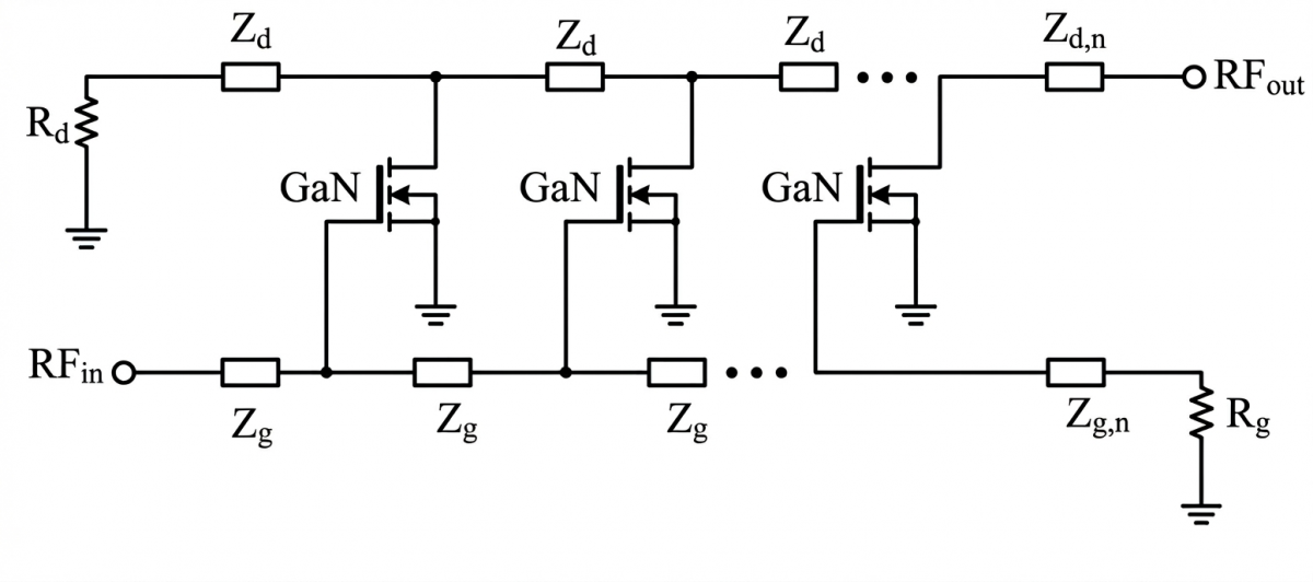
In a conventional DA, the input signal travels through the gate transmission line, exciting multiple transistor cells, and the amplified signals combine constructively through the drain transmission line. The gate and drain lines must have equal phase velocities for optimum operation so the signals add coherently at the output [18]. However, traditional DAs are limited for high-power applications because of inherent inefficiencies caused by power dissipation in termination resistors and non-uniform signal distribution among the amplifier stages. Figure 1 shows the basic structure of a DA. The input signal is transmitted along the gate line and drives multiple transistors. The output currents of these transistors are combined along the drain line. For proper operation, the phase velocities of both lines must match.
Figure 1. Typical topology of the conventional distributed power amplifiers (DPAs) with artificial transmission lines (ATLs) [14]
However, in conventional DAs, some output power is dissipated in termination resistors and the input signal is attenuated along the gate line, resulting in a non-uniform excitation of transistor cells. To overcome these limitations, the NDPA modifies the topology by removing the drain termination and by including non-uniform design parameters. The NDPA architecture features a tapered characteristic impedance for the drain transmission line and a variation of the transistor sizes along the structure. This non-uniformity enables each transistor to work closer to its optimum load, improving the output power and efficiency.
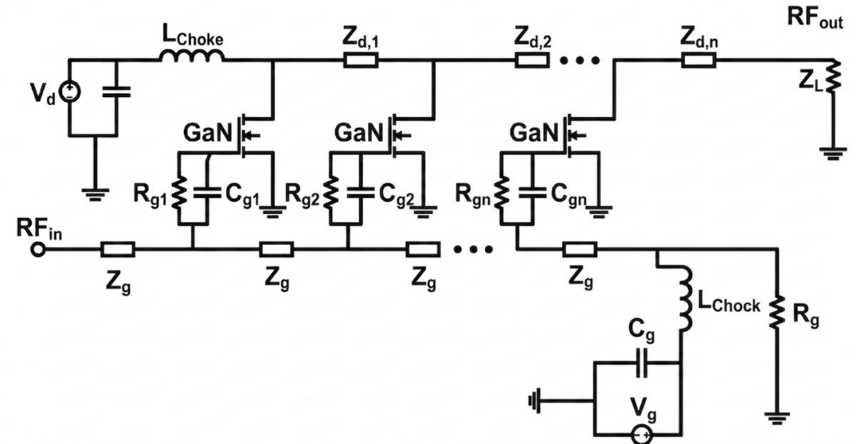
The harmonic suppression network used in this work is integrated in the gate and drain bias structures of the proposed NDPA, as shown in Figure 2. The network mainly includes a gate resistor (Rg), a gate capacitor (Cg), and an RF choke inductor (Lchock). The gate capacitor is used to compensate for the equivalent gate capacitance and to improve the cutoff frequency, while the gate resistor contributes to circuit stabilization and biasing. Moreover, the RF choke inductor helps to reduce the undesired RF harmonic components and isolate the direct current (DC) bias path from the RF signal propagation, which leads to better efficiency of power transfer and broadband operation.
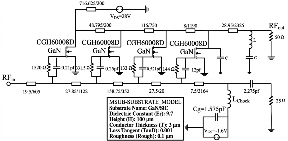
The harmonic suppression network is integrated into the practical NDPA implementation via the biasing and transmission-line sections, as shown in Figure 3. The combination of Rg, Cg = 1.575 pF and Lchock is contributive to the suppression of harmonic leakage, the improvement of circuit stability and the enhancement of overall PAE performance over the wide operation bandwidth.
It is seen that the NDPA has a circuit topology in which several transistor cells are connected by ATLs at the gate and drain. The input RF signal (RFin) propagates along the gate transmission line with a characteristic impedance Zg, exciting each of the transistors one by one. The gate ATL is made up of the gate resistors (Rg1…Rgn) representing the input impedance and the parasitic capacitances (Cgs) of the transistors and the capacitors (Cg1…Cgn). On the drain side, the amplified currents are combined along the drain transmission line with tapered impedances (Zd1, Zd2, …Zdn) for optimal load distribution and efficient power combining. The RF choke inductors (Lchock) provide the DC bias (VDS, VGs) and block RF. The load ZL consumes the combined output power (RFout) [19].
The operation of NDPA can be analyzed based on the transmission line theory and the small-signal and large-signal models of active devices. In the NDPA, a transistor cell is usually modelled as a transconductance element gm with intrinsic parasitic capacitances, which include gate source (Cgs), gate drain (Cgd) and drain–source (Cds). The parasitic components are absorbed into the ATLs that are created along the gate and drain, allowing broadband operation by distributing the amplification process by stages.
For an ideal DA with N identical stages, the voltage gain is approximately [20]:
$A_V=\frac{1}{2} g_m Z_0 N$ (1)
where, Z0 is the characteristic impedance of the transmission line. The gain is seen to increase linearly with the number of stages for negligible loss and perfect phase alignment of the gate and drain lines. However, a real NDPA implementation is corrupted by losses and non-uniformities that destroy such ideal behavior. The bandwidth of NDPA is determined by the cutoff frequency of the ATLs, which is expressed as [21]:
$f_c=\frac{1}{2 \pi \sqrt{L C}}$ (2)
where, L and C are the equivalent inductance and capacitance per section, respectively. The effective capacitance is dominated by the transistor parasitics, especially Cgs and Cds. So, the larger the device or the higher the frequency, the smaller the bandwidth can be achieved.
The NDPA has an important design feature of the tapering of the drain transmission line impedance for the proper loading of each transistor cell. In contrast to uniform DAs, the NDPA uses a position-dependent characteristic impedance Z0,n of the nth drain section, which can be approximated to be inversely proportional to the cumulative transistor periphery calculated by:
$Z_{0, n}=\frac{W_{Q i}}{\sum_{i=1}^n W_{Q i}} R_{d s}(\Omega . \mathrm{mm})$ (3)
where, Rds is the optimum output impedance per mm of the device, and WQi is the gate width of the transistor.
This reduction allows each transistor to operate closer to its optimum load resistance and thus allows for efficient power combining and improves output power and PAE. The output power of the proposed NDPA can be written as [22]:
$P_{\text {out }}=\frac{V_d^2}{2 R_L}$ (4)
where, Vd is the drain voltage swing and RL is the load impedance. The high breakdown voltage of GaN devices enables large voltage swings and the resulting high output power levels. The overall efficiency is often expressed in terms of a metric. However, in practice, the efficiency degradation is caused by the gate-line attenuation, parasitic losses and non-uniform distribution of the signals over the stages.
$P A E=\frac{P_{\text {out }}-P_{\text {in }}}{P_{D C}}$ (5)
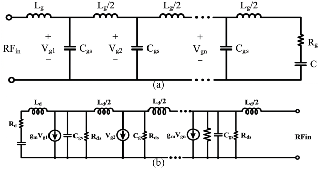
Figure 4(a) shows the simplified equivalent circuit of the gate ATL used in the proposed NDPA. The gate line is made up of distributed inductive elements along with the intrinsic gate-to-source capacitances (Cgs) of the GaN HEMT devices to form an artificial transmission structure for broadband signal propagation. The configuration allows the input RF signal to be split equally between the transistor cells while maintaining phase coherence over the operating bandwidth. The equivalent model also contains parasitic resistive and inductive elements, which cause attenuation and phase delay at high frequencies. The drain transmission line model equivalent is depicted in Figure 4(b), where drain-source capacitances (Cds) and drain inductive sections are part of the distributed network. The drain line constructively adds the amplified drain currents at the output port, which improves the output power and broadband performance. The phase synchronization between the gate and drain transmission lines is critical for coherent power addition and maximization of gain and efficiency.
Figure 4. The equivalent circuit model of the artificial transmission lines (ATLs) in the proposed non-uniform distributed power amplifier (NDPA) [14], (a) gate ATLs, and (b) drain ATLs
The proposed NDPA efficiency can be further improved by adding a harmonic suppression network at the output of the drain ATLs. In broadband DPAs, the nonlinear characteristics of the GaN HEMT device and the phase mismatch of the drain currents of the individual transistor cells may result in some of the generated RF power being at harmonic frequencies. These harmonic components do not contribute to the desired fundamental output power and therefore degrade the overall PAE.
The undesired harmonic power can be reduced with the addition of a harmonic suppression network at the drain-line output, while keeping the efficient power transfer at the fundamental frequency. This technique improves the broadband efficiency of the NDPA without greatly compromising the operating bandwidth. A similar strategy was proposed for a GaN-on-SiC NDPA covering 2–16 GHz, where a harmonic suppression network was added at the drain ATL output to improve the PAE and achieve a better trade-off between bandwidth, output power, gain and efficiency.
Broadband microwave PAs typically employ GaN-on-SiC HEMT because of their superior electrical and thermal properties compared to conventional semiconductor technologies. The work referenced states that GaN devices are very suitable for ultra-wideband DA applications because of their high breakdown voltage, high electron saturation velocity, excellent thermal conductivity and high-power density capability. GaN’s wide bandgap property enables it to operate at high drain voltages and large current densities with stable RF performance at microwave frequencies [23].
The structure is an AlGaN/GaN heterojunction on a SiC substrate. The polarization effect at the AlGaN/GaN interface results in a high-density 2DEG channel, which can offer high electron mobility and low channel resistance without intentional doping. The SiC substrate also exhibits excellent thermal conductivity, which facilitates heat dissipation during high-power operation and enhances device reliability.
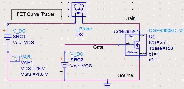
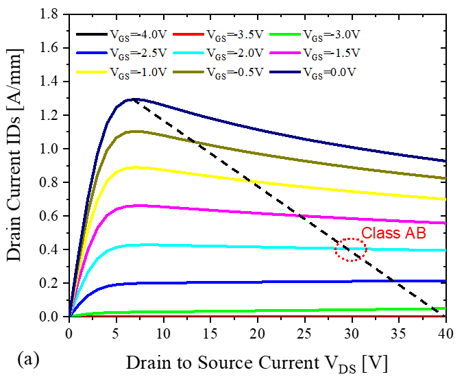
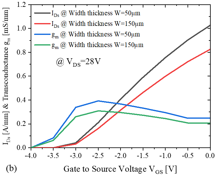
The proposed amplifier design is based on a 10 W CGH60008D 0.4 µm GaN-on-SiC HEMT process for high-frequency and power performance, as shown in Figure 5. The device was biased in Class-AB bias conditions with drain voltages of 28 V to maximize RF output swing and power density. The drain current is controlled by the VGS voltage, as demonstrated in Figure 6 and is expressed as:
$I_{D s}=g_m\left(V_{G s}-V_{t h}\right)$ (6)
where, gm is the transconductance of the device, VGS and Vth are the gate-to-source and threshold voltages, respectively. The large-signal equivalent model of GaN HEMT, besides parasitic resistances and inductances associated with gate, source and drain terminals, includes the intrinsic capacitances Cgs, Cgd and Cds. The parasitic elements are very important for the broadband amplifier performance at high frequencies.
Figure 5. The simulated direct current (DC) bias circuit design for CGH60008D 10 W GaN 0.4 µm high-electron-mobility transistor (HEMT) transistor
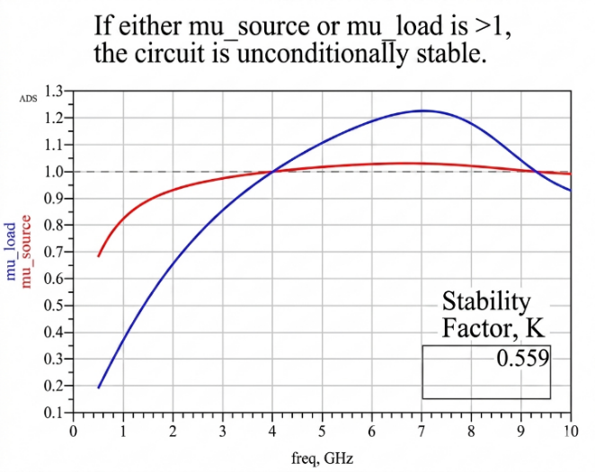
The stability performance of the proposed NDPA was evaluated by using both the Rollet stability factor (K) and μ-stability criterion over the investigated frequency range. Even though the K-factor takes values lower than unity at some frequencies, the μ-factor is still larger than one over the operating band, which means stable amplifier operation based on the μ-stability criterion. Therefore, the stability analysis in this work is mainly based on the μ-factor analysis for broadband operation [24].
Figure 7 shows the µ-stability criterion to evaluate the unconditional stability of an active microwave network within a certain frequency range. The proposed GaN device is considered unconditionally stable if and only if µ > 1, which is the minimum distance from the center of the Smith Chart to the nearest unstable region in either the source or load reflection coefficient planes. The device transitions from a potentially unstable state to an unconditionally stable state at about 4 GHz, where both µsource (red) and µload (blue) are above the unity threshold. Notably, while the K-factor is shown as 0.559 (indicating instability at that particular point), the µ curves provide a more intuitive geometric interpretation of stability margins; as the curves rise toward their peak near 7 GHz, the device becomes increasingly robust against oscillations regardless of the passive terminations applied.
The results obtained indicate that the proposed amplifier shows acceptable stability behavior in the operating frequency range. The main measure for assessment of unconditional stability in the proposed broadband NDPA design was the μ-factor criterion.
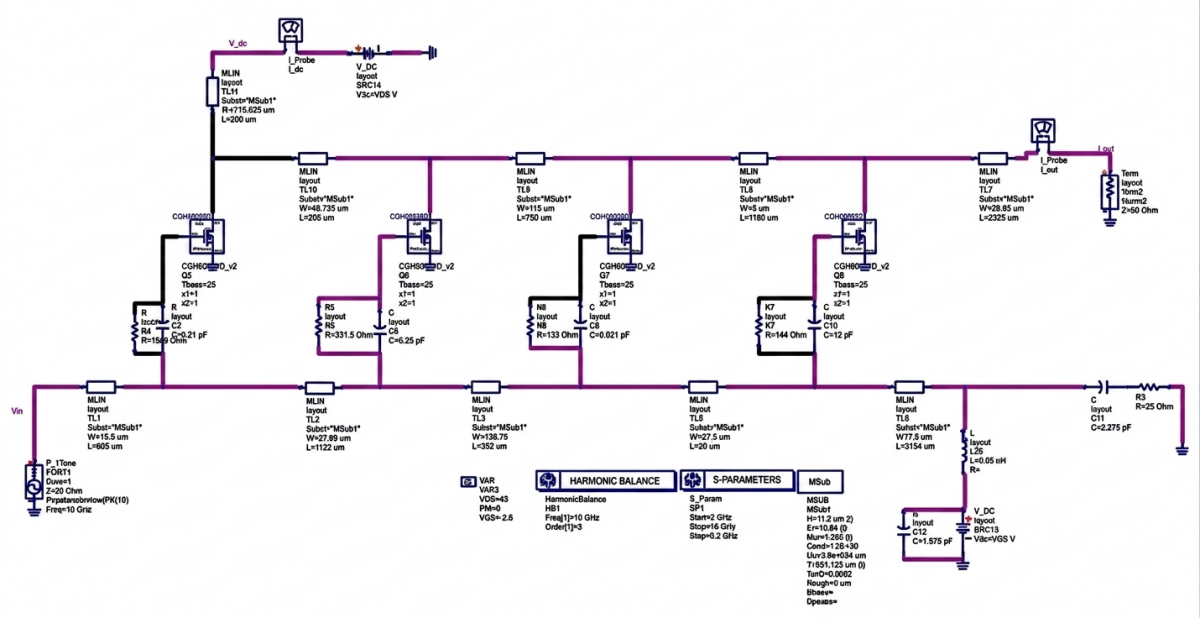
The performance of the proposed GaN-based NDPA was evaluated in terms of broadband gain response, output power capability, PAE and stability behavior. The design strategy is mainly based on overcoming the efficiency limitations of the conventional DAs by using a non-uniform drain transmission line, tuned transistor loading and an additional harmonic suppression concept at the drain-line output. To reduce the harmonic power loss and to improve the overall PAE over a wide operating band, a harmonic suppression network was inserted at the output of the drain ATL. The proposed NDPA structure was designed and analyzed by using the Advanced Design System (ADS) simulation software, as shown in Figure 8. The ADS-based schematic was used to model the 10 W CGH60008D 0.4 µm GaN-on-SiC HEMT transistor cells, gate and drain ATLs, biasing networks and non-uniform drain-line impedance tapering to evaluate the broadband performance of the proposed amplifier.
The proposed design includes a concept of harmonic suppression to reduce unwanted harmonic power components and to improve the effective transfer of power at the fundamental frequency. However, the study is limited to evaluating the overall performance of broadband amplifiers using circuit-level simulations.
To highlight the contribution of each design technique, an ablation study was carried out by comparing four configurations: (i) a uniform DA baseline, (ii) a non-uniform tapered ATL design without harmonic suppression, (iii) a uniform design with harmonic suppression, and (iv) the proposed NDPA combining tapered ATLs and harmonic suppression. The comparison shows that the tapered ATL structure improves the broadband load distribution and output power, while the harmonic suppression network helps to mitigate the undesired harmonic power and improve PAE. The best overall performance is achieved when both techniques are combined.
The simulated GaN HEMT characteristics confirm the suitability of GaN-on-SiC technology for broadband high PA applications. The complete circuit-level implementation of the proposed NDPA is shown in Figure 8. The chosen artificial transmission-line topology can be directly implemented in a physical microwave layout using appropriate MMIC or PCB technologies. Therefore, the presented design provides a practical basis for future electromagnetic optimization, fabrication and measurement.
The device supports high-drain voltage operation under Class-AB biasing and provides controllable drain current and transconductance through gate bias adjustment. These features allow a practical trade-off between efficiency, linearity and output power, while the stability results demonstrate reliable operation at higher frequencies. The NDPA topology proposed in this work is a step forward from conventional DAs at the circuit level, as it reduces power losses due to termination resistors and gate-line attenuation. The tapered drain-line impedance enables closer operation of each transistor cell to its optimum load condition, which leads to more efficient drain-current combining and hence improved broadband output power and PAE.
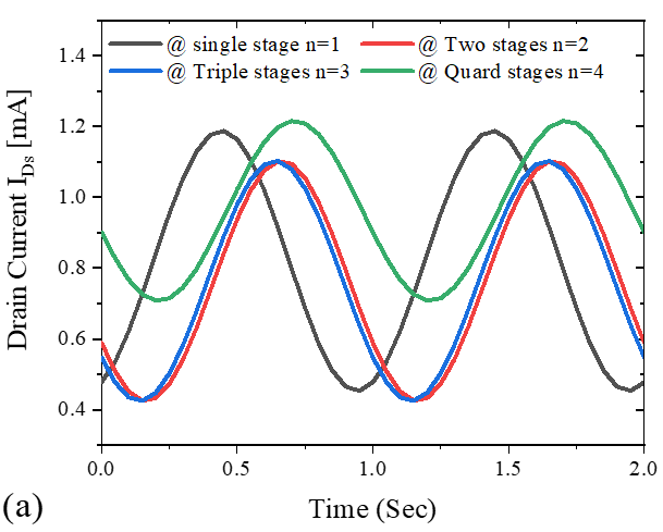
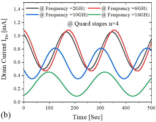
The simulated drain current (IDs) characteristics of the proposed GaN-based NDPA using a 10 W CGH60008D 0.4 μm GaN-on-SiC HEMT transistor are shown in Figure 9. From Figure 9(a), the drain current increases gradually from about 0.45 mA in the first stage (n = 1) to about 1.3 mA in the fourth stage (n = 4), which confirms the effective current combining and normal operation of the non-uniform drain ATL structure. The in-phase relationship between stages encourages constructive current summation and improves the amplifier output power capability. Figure 9(b) shows the output-stage drain current response over the 2–16 GHz frequency range. The current amplitude is around 1.1 mA at 2 GHz and 6 GHz, reduces to approximately 0.8 mA at 10 GHz, and then further drops to about 0.45 mA at 16 GHz due to the increased parasitic effects, transmission-line losses, and the reduced transistor gain at higher frequencies. The obtained results show that the proposed non-uniform distributed architecture is capable of efficient broadband current combining, providing improved output power and efficiency performance in the practical operating frequency range of the CGH60008D device.
Figure 9. The simulated time-frequency behavior of drain currents (IDs) in the proposed gallium nitride (GaN)-based non-uniform distributed power amplifier (NDPA): (a) IDs at each stage from n = 1 to 4, and (b) IDs at the output stage
The proposed GaN-based NDPA, by using ATLs, non-uniform drain-line structure and harmonic suppression techniques, provides a better trade-off between broadband bandwidth, gain, output power and efficiency compared to traditional DA architectures. The ATLs effectively absorb the parasitic capacitances of the GaN HEMT devices, extending the operating bandwidth and reducing high-frequency gain degradation, and the non-uniform drain-line configuration improves load distribution and minimizes power losses resulting from reverse current flow. Moreover, suitable gate-bias selection helps to reach balanced amplifier performance in terms of gain, linearity, efficiency, and broadband impedance matching.
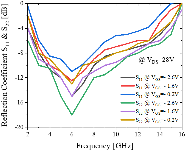
These unwanted harmonics can be filtered at the output stage to give higher power at the fundamental frequency and so improve the amplifier efficiency. The electromagnetic simulation results of the proposed GaN-based NDPA, including the small- and large-signal analysis at the layout level, in the frequency range of 2–16 GHz, were conducted. Figure 10. Simulated small-signal reflection coefficients S11 and S22 for different gate bias voltages VGS = −0.2 V, −1.6 V and −2.6 V at a constant drain bias voltage VDS = 28 V. The results show that the broadband impedance matching of the amplifier is acceptable over most of the operating band, with both S11 and S22 under −10 dB, with the best matching performance around 5–7 GHz. In particular, the response of the S22 is very close to −18 dB at VGS = −2.6 V, which means the reflected power is reduced and the output matching is improved. However, the reflection coefficients slowly increase at higher frequencies approaching 16 GHz due to parasitic effects and limits of the transmission line. In this work, the optimum operating point was chosen at VGS = −1.6 V, which provides a good compromise between broadband matching performance, amplifier stability, gain characteristics and linearity compared to other bias conditions. In brief, the proposed NDPA provides stable broadband small-signal operation and good impedance matching for ultra-wideband microwave applications.
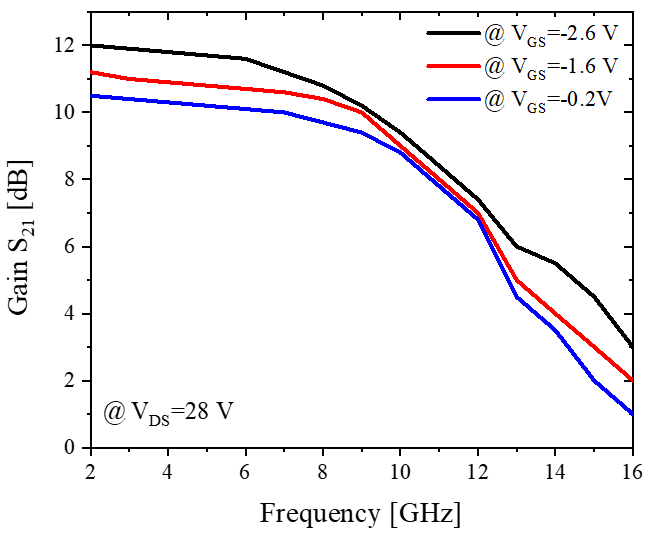
The large-signal results show the effective operation of the proposed GaN-based NDPA in the 2–16 GHz broadband range. Figure 11 shows the simulated gain response (S21) at different gate bias voltages at VDS = 28 V. The amplifier exhibits a maximum gain of approximately 11.2 dB at lower frequencies. The gain gradually decreases with increasing frequency due to transmission-line losses and parasitic effects, reaching approximately 2.2 dB at 16 GHz. The gain at the selected operating bias VGS = −1.6 V is about 11.2 dB at 2 GHz and about 2.2 dB at 16 GHz. The amplifier gain decreases gradually with the increase of frequency because of parasitic effects and transmission line losses at high frequencies. In this work, the optimal operating point with a good compromise of gain performance, stability, linearity and efficiency for broadband operation was VGS = −1.6 V.
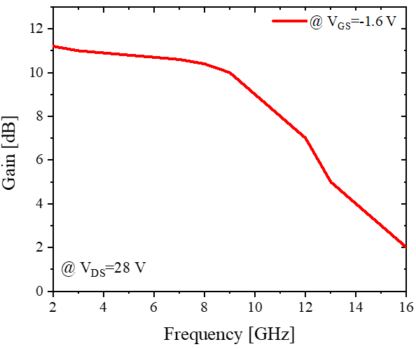
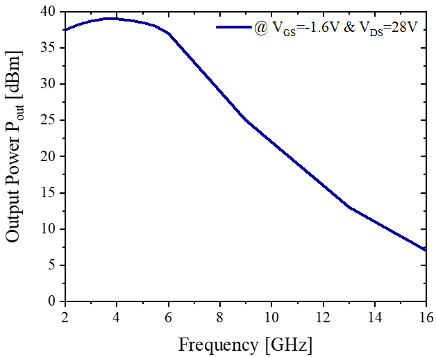
The simulated gain performance of the proposed 10 W CGH60008D 0.4 µm GaN-on-SiC HEMT process-based NDPA at the selected operation bias condition of −1.6 V and VDS = 28 V is shown in Figure 12. From the figure, we can see that the amplifier has a broadband gain of about 11.2 dB at low frequencies and stable amplification performance in the 2–16 GHz working range. The gain decreases gradually with frequency due to parasitic capacitances and transmission line losses, and reaches about 2.2 dB at 16 GHz. Figure 13 shows the output power performance at a fixed input power below 20 dBm. The amplifier obtains a saturated output power from about 35 dBm to 39 dBm at lower frequencies and has good power stability over the broadband operating range. But at higher frequencies, the output power decreases gradually due to higher losses and lower transistor gain near the upper frequency limit.
Figure 12. The simulated power gain of the proposed non-uniform distributed power amplifiers (NDPAs) based on GaN high-electron-mobility transistor (HEMT) at VGS = −1.6 V and VDS = 28 V for broadband applications
Figure 13. The simulated output power of the proposed non-uniform distributed power amplifiers (NDPAs) based on GaN high-electron-mobility transistor (HEMT) at VGS = −1.6 V and VDS = 28 V for broadband applications with a frequency range of 2–16 GHz
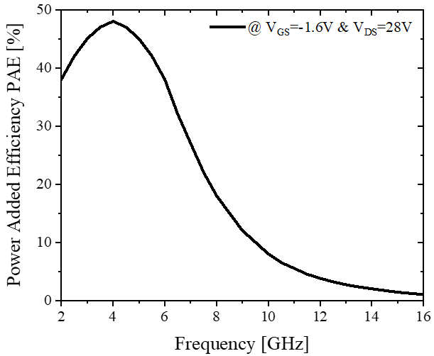
Figure 14 presents the PAE performance of the proposed amplifier under the same bias condition. The results show that the PAE reaches a maximum value of 48% at around 4 GHz and then gradually decreases with increasing frequency, falling to low values near 16 GHz. This behavior is mainly due to higher parasitic effects and lower matching efficiency at high frequencies. The obtained results confirm that the use of tapered drain ATLs in combination with the harmonic suppression technique provides an effective trade-off between broadband gain, output power and efficiency, thus improving the overall performance of the GaN-based NDPA for ultra-wideband microwave applications. The improved PAE performance is due to the synergistic effects of the non-uniform drain-line architecture, the optimized transmission-line design, the broadband impedance matching, and the harmonic suppression strategy. Thus, the improvement in efficiency should be seen as the result of the overall amplifier architecture rather than of a single design element.
Figure 14. The simulated power added efficiency (PAE) of the proposed non-uniform distributed power amplifiers (NDPAs) based on GaN high-electron-mobility transistor (HEMT) at VGS = −1.6 V and VDS = 28 V for broadband applications with a frequency range of 2–16 GHz
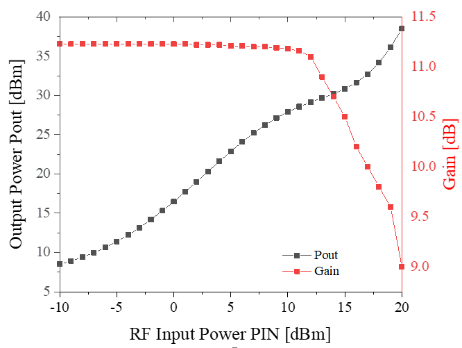
The simulated output power and gain performances of the proposed GaN-based NDPA versus RF input power (PIN) are shown in Figure 15. The results indicate that the output power (Pout) increases gradually with the increase of the input power, increasing from about 8 dBm at PIN = −10 dBm to almost 38 dBm at PIN = 20 dBm. This behavior demonstrates the effectiveness of the power amplification capability of the proposed amplifier in broadband operation. On the other hand, the gain is fairly constant at around 11.2 dB for most of the operating range and then begins to decline at higher input power levels because of gain compression and the onset of saturation effects. The gain reduction becomes more noticeable beyond PIN = 14 dBm, where the amplifier is approaching its nonlinear operating region. The results show that the proposed NDPA provides a good compromise between the gain stability and the output power enhancement for high-power microwave applications.
Figure 15. The simulated Pout and gain of the proposed non-uniform distributed power amplifiers (NDPAs) based on GaN HEMT at VGS = −1.6 V and VDS = 28 V as a function of RF input power (PIN) for broadband applications
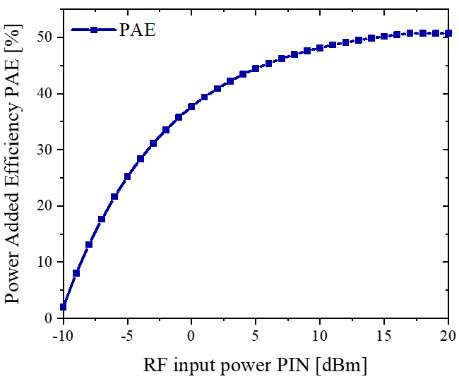
The simulated PAE of the proposed amplifier versus RF input power is shown in Figure 16. The PAE is found to increase exponentially with increasing PIN from about 2% at low input power levels to a maximum value of about 50% at PIN = 20 dBm. This trend shows that the amplifier is working more efficiently as the RF drive level increases and the transistor gets close to its optimum large-signal operating condition. The efficiency increase is smooth and confirms the efficiency effectiveness of the non-uniform drain-line architecture and harmonic suppression network to reduce the power losses and improve RF power conversion efficiency. Thus, the obtained results confirm the high-efficiency broadband operation of the proposed GaN-based NDPA with improved output power performance suitable for ultra-wideband RF and microwave systems.
Figure 16. The simulated power added efficiency (PAE) of the proposed non-uniform distributed power amplifiers (NDPAs) based on GaN HEMT at VGS = −1.6 V and VDS = 28 V as a function of RF input power (PIN) for broadband applications
The conventional configuration was implemented by not applying the harmonic suppression network to quantitatively evaluate the contribution of the network. A comparison between both cases is summarized in Table 1. The addition of the harmonic suppression network is observed to significantly improve the performance of the amplifier. In particular, the maximum PAE increases from 41% to 48%, corresponding to an improvement of 17.1%, and the saturated output power increases from 37.5 dBm to 39 dBm. Furthermore, the broadband operation range of 2–16 GHz is preserved and a small gain enhancement in the small-signal regime is obtained. These results demonstrate that the harmonic suppression network can substantially reduce the harmonic power losses and improve the RF power conversion efficiency while keeping the broadband features of the proposed amplifier.
Table 1. Performance comparison of the proposed NDPAs with and without the harmonic suppression network technique
|
Parameters |
Conventional NDPAs |
Proposed NDPAs |
Improvement |
|
Max. PAE, % |
41 |
48 |
+17.3% |
|
Saturated output power, dBm |
37.5 |
39 |
+1.5 |
|
Gain, dB |
10.8 |
11.2 |
+0.4 |
|
Bandwidth, GHz |
2–16 |
2–16 |
---- |
|
Harmonic leakage |
Higher |
Reduced |
Improved |
Note: PAE = power-added efficiency, NDPA = non-uniform distributed power amplifier.
Table 2 shows the performance comparison between the proposed NDPA and some recently reported DPAs in the literature. The proposed design is based on a 10 W CGH60008D 0.4 μm GaN-on-SiC HEMT process with a harmonic suppression network and operates in a wide frequency range, 2–16 GHz. The comparison demonstrates that the proposed amplifier obtains a good trade-off among bandwidth, output power, gain and PAE compared with previous works. Some reported designs provide higher output power or efficiency, but operate over narrower bandwidths or use different fabrication technologies. Therefore, the proposed non-uniform distributed architecture coupled with harmonic suppression techniques realizes effective broadband performance, and the amplifier is suitable for ultra-wideband microwave and RF applications.
Table 2. Performance comparison of the proposed non-uniform distributed power amplifiers (NDPAs) based on 10 W CGH60008D 0.4 µm GaN-on-SiC high-electron-mobility transistor (HEMT) process with other literature reviews
|
Ref. |
Frequency [GHz] |
Technology |
Gate Length [µm] |
Pout [dBm] |
Gain [dB] |
PAE [%] |
Area [mm2] |
|
[9] |
6–18 |
Modified NDPA based on a large-sized GaN transistor |
0.25 |
38–41.6 |
8–12 |
13–33.8 |
8.50 |
|
[14] |
2–16 |
NDPA based on GaN with a harmonic suppression network |
0.25 |
35–37 |
9.1–11.6 |
16.6–27 |
4.00 |
|
[15] |
3.5–15 |
NDPA based on GaN with a modified gate-line structure |
0.12 |
35–36 |
10–14 |
28–45 |
11.00 |
|
[25] |
4–16 |
NDPA based on a commercial GaN process |
0.15 |
38–40 |
8.7–14 |
11.8–33.9 |
7.80 |
|
[26] |
6–18 |
NDPA based on MMIC GaN-on-SiC HEMT with asymmetric impedance transformer |
0.25 |
42–44 |
10–12 |
15–24 |
1.54 |
|
[27] |
18–42 |
NDPA based on MMIC GaN-on-SiC HEMT |
0.10 |
33 |
8–10 |
15 |
3.20 |
|
[28] |
2–12 |
Compact GaN MMIC NDPA |
0.25 |
37–39.3 |
9–14 |
5–35 |
4.30 |
|
[29] |
0.1–8 |
Distributed GaN MMIC PA |
0.25 |
40 |
10–12 |
8–25 |
6.20 |
|
[30] |
4–16 |
Traditional GaN DPAs |
0.15 |
38–40 |
8.7–14 |
11.8–33.9 |
7.80 |
|
This work |
2–16 |
NDPA based on GaN-on-SiC HEMT with harmonic suppression network |
0.40 |
35–39 |
2.2–11.2 |
48 |
16.00 |
Note: GaN-on-SiC = gallium nitride on silicon carbide.
The proposed GaN-based NDPA with 10 W CGH60008D 0.4 μm GaN-on-SiC HEMT transistor achieved effective broadband performance from 2–16 GHz. The proposed architecture utilized tapered drain ATLs coupled with a harmonic suppression network to achieve improved gain, output power and PAE compared with the conventional DA structures. The simulated results showed stable small-signal gain from 11.2 dB to 2.2 dB with the output power from 35 dBm to 39 dBm and a maximum PAE of 48% around 4 GHz. In addition, the selected Class-AB bias operating point (VGS = −1.6 V, VDS = 28 V) provided a good compromise between gain performance, efficiency, linearity, and broadband impedance matching. The achieved results validated that the proposed NDPA structure efficiently decreases the harmonic power losses and enhances the broadband RF power amplification performance, which is applicable for ultra-wideband microwave and modern wireless communication applications. The present work is limited to circuit-level simulation and analysis, but the results obtained show the feasibility of the proposed architecture for broadband applications. Future work will focus on layout implementation, full-wave electromagnetic verification, fabrication and experimental characterization of the proposed amplifier.
The authors would like to express their sincere gratitude to both the Departments of Communications and Intelligent Digital Systems Engineering, University of Mosul, for providing the technical resources and support necessary to carry out this research.
|
ATLs |
Artificial transmission lines |
|
Cds |
Drain to source capacitor, pf |
|
Cgs |
Gate to source capacitor, p |
|
DAs |
Distributed power amplifiers |
|
GaN |
Gallium nitride |
|
gm |
Transconductance, S |
|
HEMT |
High electron mobility transistor |
|
MMIC |
Monolithic microwave integrated circuit |
|
NDPA |
Non-uniform distributed power amplifier |
|
PAE |
Power added efficiency, % |
|
Greek symbols |
|
|
µ |
Electron mobility, cm2/(V·s) |
|
π |
Mathematical constant |
|
Subscripts |
|
|
fo |
Cut off frequency, Hz |
|
Vout |
Output voltage, V |
|
RF |
Radio frequency, Hz |
[1] Miličević, Z.M., Bojković, Z.S. (2024). Review of 5G and 6G applications for mobile wireless communication in the military environment. Vojnotehnički Glasnik/Military Technical Courier, 72(1): 435-451. https://doi.org/10.5937/vojtehg72-47037
[2] Orr, G., Azoulay, M., Golan, G., Burger, A. (2025). Gallium nitride high-electron-mobility transistor-based high-energy particle-detection preamplifier. Metrology, 5(2): 21. https://doi.org/10.3390/metrology5020021
[3] Lu, H., Zhang, M., Yang, L., et al. (2025). A review of GaN RF devices and power amplifiers for 5G communication applications. Fundamental Research, 5(1): 315-331. https://doi.org/10.1016/j.fmre.2023.11.005
[4] Hima Bindhu, S.K., Verma, Y.K., Bhatia, K. (2026). Recent advancements in high electron mobility transistor-based monolithic microwave integrated circuits: A review. In Smart Chips for Smart Devices: VLSI Design for Next-Generation IoT Solutions, pp. 179-190. https://doi.org/10.1002/9781394335831.ch9
[5] Guo, T., Liu, Q.B., Xi, Z.Z., Wang, H., Wei, H.L., Wang, W. (2025). An adaptive wide-band impedance matching network for frequency-domain electromagnetic method transmitter systems. IEEE Transactions on Industrial Electronics, 73(1): 253-264. https://doi.org/10.1109/TIE.2025.3594444
[6] Hassani, S., Chen, C.H., Nikolova, N.K. (2024). Design of impedance matching network for low-power, ultra-wideband applications. Journal of Low Power Electronics and Applications, 14(1): 16. https://doi.org/10.3390/jlpea14010016
[7] Saeed, S.R., Kareem, A.R., Hameed, A.Q. (2023). An enhanced design of cascaded single-stage distributed amplifiers utilizing quasi-differential amplifier cells. Mathematical Modelling of Engineering Problems, 10(4): 1281-1287. https://doi.org/10.18280/mmep.100421
[8] Hussein, S.H., Yaseen, M.T., Hamid, K.H. (2025). Design and implementation of MMIC power amplifiers for modern wireless communication systems. Journal of Engineering Science and Technology, 20(3): 654-669.
[9] Kim, J., Kwon, Y. (2020). A high-performance GaN-modified nonuniform distributed power amplifier. IEEE Transactions on Microwave Theory and Techniques, 68(5): 1729-1740. https://doi.org/10.1109/TMTT.2020.2972277
[10] Sun, Y., Benosman, M., Ma, R. (2022). GaN distributed RF power amplifier automation design with deep reinforcement learning. In 2022 IEEE 4th International Conference on Artificial Intelligence Circuits and Systems (AICAS), Incheon, South Korea, pp. 54-57. https://doi.org/10.1109/AICAS54282.2022.9869961
[11] Nguyen, L., Pham, A.N., Lee, S., Huynh, C. (2021). A broadband, high even-order suppression distributed power amplifier for sub-6 GHz communication system. In 2021 International Symposium on Electrical and Electronics Engineering (ISEE), Ho Chi Minh, Vietnam, pp. 20-25. https://doi.org/10.1109/ISEE51682.2021.9418689
[12] Wang, W.B., Xin, Z.Y., Jiang, Y. (2024). A 41.2-dBm 2-18-GHz GaN MMIC non-uniform distributed power amplifier for wideband communication applications. In 2024 IEEE MTT-S International Microwave Workshop Series on Advanced Materials and Processes for RF and THz Applications (IMWS-AMP), Nanjing, China, pp. 1-3. https://doi.org/10.1109/IMWS-AMP62793.2024.10966573
[13] Ismael, A.A., Younis, A.T., Abdo, E.A., Hussein, S.H. (2021). Improvement of non-linear power amplifier performance using Doherty technique. Journal of Engineering Science and Technology, 16(6): 4481-4493.
[14] Luan, T.Y., Leng, Y.Q., Qiu, X., et al. (2022). Design of 2–16 GHz non-uniform distributed GaN HEMT MMIC power amplifier with harmonic suppression network. Applied Sciences, 12(21): 11077. https://doi.org/10.3390/app122111077
[15] Veisee, S., Liu, R., Zhu, A. (2024). An efficiency-enhanced GaN MMIC nonuniform distributed power amplifier using a modified gate line structure. IEEE Transactions on Microwave Theory and Techniques, 73(6): 3503-3513. https://doi.org/10.1109/TMTT.2024.3499753
[16] Hussein, S.H., Mohammed, K.K. (2023). A dual-band compact integrated rectenna for implantable medical devices. International Journal of Electronics and Telecommunications, 69(2): 239-245. https://doi.org/10.24425/ijet.2023.144356
[17] Srivastava, G., Kumar, S. (2021). A state-of-the art review on distributed amplifiers. Wireless Personal Communications, 117(2): 1471-1525. https://doi.org/10.1007/s11277-020-07932-9
[18] Hussein, S.H., Al-Rawe, M.A.A. (2020). Real time speed control of the DC motor in LabVIEW. In 2020 7th International Conference on Electrical and Electronics Engineering (ICEEE), Antalya, Turkey, pp. 137-141. https://doi.org/10.1109/ICEEE49618.2020.9102625
[19] Podgorski, A.S., Wei, L.Y. (1982). Theory of traveling-wave transistors. IEEE Transactions on Electron Devices, 29(12): 1845-1853. https://doi.org/10.1109/T-ED.1982.21040
[20] Zhang, F., Kinget, P.R. (2006). Low-power programmable gain CMOS distributed LNA. IEEE Journal of Solid-State Circuits, 41(6): 1333-1343. https://doi.org/10.1109/JSSC.2006.874283
[21] Shin, D.H., Yom, I.B., Kim, D.W. (2017). 6-GHz-to-18-GHz AlGaN/GaN cascaded nonuniform distributed power amplifier MMIC using load modulation of increased series gate capacitance. ETRI Journal, 39(5): 737-745. https://doi.org/10.4218/etrij.17.0116.0737
[22] Pang, B., You, F., Pang, T.T., Qin. R.X., Xiao. Z.H., Liu, Y.J. (2026). A 2–18 GHz high-efficiency CMOS nonuniform distributed power amplifier with a novel reconfigurable inductive termination. IEEE Journal of Solid-State Circuits, pp. 1-12. https://doi.org/10.1109/JSSC.2026.3665920
[23] Han, G., Kim, J., Park, S., Bae, W. (2025). Thermal management of wide-bandgap power semiconductors: Strategies and challenges in SiC and GaN power devices. Electronics, 14(21): 4193. https://doi.org/10.3390/electronics14214193
[24] Wang, C.T., Liao, X.J., Gong, M.Q., et al. (2026). A 6–18 GHz high-efficiency GaN power amplifier using transistor stacking and reactive matching. Micromachines, 17(3): 338. https://doi.org/10.3390/mi17030338
[25] Mahon, S.J., Milner, L.E., Shahid, I., Parker, A.E., Gorman, M.C., Heimlich, M.C. (2021). High power density 4 to 16 GHz non-uniform distributed power amplifier with a novel trifilar. In 2020 15th European Microwave Integrated Circuits Conference (EuMIC), Utrecht, Netherlands, pp. 273-276.
[26] Kim, J. (2026). Ultra-wideband asymmetric impedance transformer design for high-power amplifier MMICs. Journal of Electromagnetic Engineering and Science, 26(1): 1-9. https://doi.org/10.26866/jees.2026.1.r.335
[27] Luong, G., Ouarch, Z., Serru, V., Driad, S., Madel, M. (2026). Ultra-wideband 18–42 GHz, 2W, 15% PAE distributed power amplifier MMIC on 0.1 µm GaN-on-SiC for advanced wireless systems. In 2026 IEEE Topical Conference on RF/Microwave Power Amplifiers for Radio and Wireless Applications (PAWR), pp. 21-24. https://doi.org/10.1109/PAWR69496.2026.11408559
[28] Ersoy, E., Chevtchenko, S., Kurpas, P., Heinrich, W. (2014). A compact GaN-MMIC non-uniform distributed power amplifier for 2 to 12 GHz. In Proceedings of the German Microwave Conference (GeMiC), Aachen, Germany, pp. 1-3.
[29] Moon, J.S., Kang, J., Brown, D., et al. (2017). 100 MHz–8 GHz linear distributed GaN MMIC power amplifier with improved power-added efficiency. In Proceedings of the IEEE Topical Conference on RF/Microwave Power Amplifiers for Radio and Wireless Applications (PAWR), Phoenix, AZ, USA, pp. 40-43. https://doi.org/10.1109/PAWR.2017.7875568
[30] Roberg, M., Schafer, S., Marrufo, O., Hon, T. (2019). A 2–20 GHz distributed GaN power amplifier using a novel biasing technique. In 2019 IEEE MTT-S International Microwave Symposium (IMS), Boston, MA, USA, pp. 694-697. https://doi.org/10.1109/MWSYM.2019.8700748