Ahmed Kahlouche* | Mounir Bouras | Abdessalem Hocini
© 2022 IIETA. This article is published by IIETA and is licensed under the CC BY 4.0 license (http://creativecommons.org/licenses/by/4.0/).
OPEN ACCESS
Nowadays, sensor technology has attracted great interest in various domains. In this work, we have analyzed a one dimensional phononic crystal made by the stack of N bilayers of (LiNbO3/SiO2). The sensor design consists of a one dimensional phononic crystal structure with a defect layer inserted in the middle. Using the Transfer Matrix Method (TMM), the transmission spectrums of acoustic waves are calculated and plotted. In this work, we are interested in the resonance peak that is transmitted inside the phononic band gap. The results obtained show clearly that the resonant frequency of the measured transmission peak is very sensitive to the layer defect properties. This proves that such structure offers a new platform for sensing applications.
1D phononic crystal, band gaps, transfer matrix method (TMM), sensors materials, acoustic waves
Phononic crystals (PnCs) are a novel type of artificial materials that exhibit periodic distributions in their densities and mechanical properties in one, two or three dimensions of space [1, 2]. Such crystals help to guide, control, and modify the transmission of acoustic and elastic waves in fluids and solids, respectively. An interesting feature of these structures is the formation of phononic band gaps, which prohibit the propagation of elastic/acoustic waves in certain directions and frequency ranges. These phononic band gaps have the same behavior as photonic band gaps with respect to the propagation of electromagnetic waves in photonic crystal structures [3, 4]. Phononic bands are created principally by spatial modulation of the acoustic impedance of the materials that compose the structure. Therefore, when designing phononic crystal structures, geometrical and physical parameters such as fill factor, mass density, sound speed, and angle of incident must be considered [5-9].
In recent years, phononic crystal structures have attracted considerable interest due to their potential applications in various technological fields, such as acoustic filtering, cavities, waveguides, barriers sonic and sensors [10-14]. On the other hand, great attention concerns the multilayer phononic structures, which have been widely studied and proposed as new configurations for measuring the acoustic properties of fluids [15-18]. The characterization of these sensors is commonly based on the resonance frequency, transmission ratio, or width of the transmission peak [15, 19-21]. In this work, the resonance frequency of the defect mode is used to detect changes in the defect layer properties, especially the thickness. Firstly, we have studied the propagation of the longitudinal acoustic waves through a regular one-dimensional phononic crystal in order to determine the phononic band gaps. Secondly, a special interest was devoted to the phenomenon of local resonance inside the phononic band gap in order to use such a structure for sensing the variations in thickness of the layer defect. The transmission coefficients are calculated and plotted by using the Transfer Matrix Method (TMM), which is usually adopted for multilayer structures [15, 22-24].
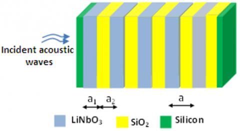
The proposed 1D-PnC structure is shown in Figure 1. The structure consists of five unit cells. Each unit cell is composed of two different materials; LiNbO3 and SiO2 with thicknesses a1=aLiNbO3= 0.5 mm and a2=aSiO2= 0.5 mm respectively. The lattice constant of every unit cell is a=a1+a. In this work, we used the transfer matrix method to study the acoustic/elastic wave propagation in one-dimensional phononic crystal. TMM is based on the calculation of the transmission or reflection coefficients.
Figure 1. A schematic diagram of a perfect 1D-phononic crystal structure
For a longitudinal acoustic wave with normal incidence on the phononic crystal, the pressure of the acoustic wave in the medium is governed by the following equation:
$\nabla^{2} \emptyset=\frac{1}{C_{l}^{2}} \frac{\partial^{2} \emptyset}{\partial t^{2}}$ (1)
where, Ø is the displacement and Cl is the longitudinal speed of sound in each layer [22-24]. The elastic constants of the matrix and of the inclusions constituting the 1D crystal are illustrated in Table 1 [25].
Table 1. The elastic properties of materials
|
Material |
Density $\rho$(Kg/m3) |
Transverse Celerity Ct (m/s) |
Longitudinal Celerity Cl (m/s) |
|
LiNbO3 |
4674 |
4030 |
6574 |
|
SiO2 |
2600 |
3370 |
5840 |
|
Silicon |
2330 |
5359 |
8950 |
3.1 1D Phononic band gap
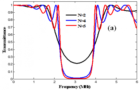
First, we consider the one dimensional perfected phononic structure illustrated in Figure 1. We also consider the propagation of longitudinal elastic waves across the structure. Figure 2(a) shows the transmission spectrum as a function of the frequency obtained with the TMM for 2, 4 and 5 unit cells. It’s clear that the number of oscillations on the left and right sides of the gap depends on the number of unit cells. On the other hand, the transmittance in the gap decreases sharply to 0% for a high number of cells. Figure 2(b) shows the variations of the band gap width and location as a function of the filling ratio.
Figure 2. (a) Transmission spectrum for a 1D-PnC for 2, 4 and 5 unit cells; (b) Variations of phononic bandgap width as a function of the filling fraction ratio
The value of the gap width of the first band increases with the increase of the value of the LiNbO3 material thickness aLiNbO3 (a1) until it reaches a critical value and then decreases. The largest phononic band gap appears at a filling factor of ff = 0.50. For this value, the frequency of the band gap goes from 2.251 MHz to 3.935 MHz. Then, as the filling ratio of any layer increases to the critical value, the cutoff frequencies of the higher modes of the incident wave also decrease until the band is completely closed. Therefore, the value of the filling fraction of any materials is necessary to obtain a wide bandgap, which prevents the propagation of waves.
In this section, we will study the influence of the acoustic impedance defined by the product of the density and speed of sound on the size and location of the phononic band gaps.
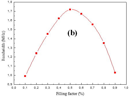
Figure 3. Width and position of 1D phononic band gap as a function of density contrast and speed of sound for 5 unit cells
Figure 3 reports the variations in the phononic band gap ∆f (MHz) and band position f0 (MHz) as a function of mass density contrast (red and blue curves, respectively). While the green and black curves show the influence of the longitudinal velocity contrast on the properties of the phononic band gap. The results clearly demonstrate that the density and the longitudinal velocity of sound have a great influence on the location (f0) and the width (∆f) of the phononic band gap.
The obtained results can be explained as follows, more the ratio between the acoustic impedance of the two materials constituting the structure, the speed of the waves at the interfaces is modified, which leads to the formation of a forbidden band. Therefore, a good ratio between the acoustic impedance and a good filling factor can lead to the appearance of a band gap in which the propagation of acoustic or elastic waves is not allowed.
3.2 Sensing the thickness
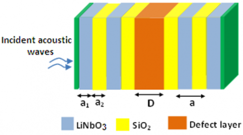
In order to use our structure as a thickness sensor. In the present section, we are studying the influence of the thickness of the defect layer on the phononic band properties. Our design [(LiNbO3/SiO2)2/(defect)/(LiNbO3/SiO2)2], is a defective one dimensional phononic structure composed of two different layers of (LiNbO3/SiO2) repeated in N=4 unit cells with equal thickness. The defect material is a layer of LiNbO3 with a thickness of D =1 mm. It is inserted in the middle of the periodic structure to form a mirror around it, as shown in Figure 4.
Figure 4. A schematic diagram of a defect 1D-PnC structure
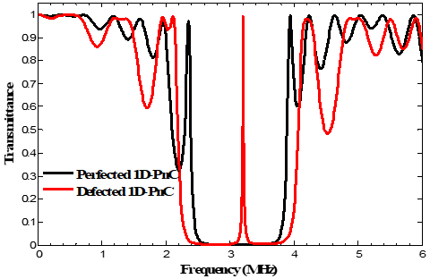
In contrast to the periodic structure, the insertion of a defect layer in a periodic structure induces the breaking of the periodicity of the crystal, which causes a different interaction with the acoustic wave. Therefore, a phenomenon of localization of the acoustic wave inside the band gap appeared. The transmission spectrum of the defected 1D-PnC structure obtained with TMM is shown in Figure 5.
Figure 5. Transmission spectrum of a defected 1D-PnC with geometrical defect
According to the results, the phononic band has expanded and a defect mode with intensity nearly equal to 100% has appeared inside the phononic band gap at the reference frequency f=3.2 MHz. The transmitted peak within the phononic band gap is caused by wave localization within the defect layer. The basic idea in the process of detecting changes in the defect layer parameters is usually the resonant frequency of the defect mode.
Based on the resonant frequency of the defect mode of our defected phononic crystal structure, we will study now the influence of the defect thickness on the resonant mode (RM) appeared inside the phononic band gap.
Figure 6(a) shows the effects of the thickness changes on the resonant mode. We can observe that the thickness of the defect layer has a pronounced influence on the resonance frequency of the transmitted peak. Thus, by increasing the thickness D from 0.85 mm to 1.15 mm, the position of resonant mode (f0) can be adjusted inside the band gap. Figure 6(b) shows the relationship between the thickness of the defect layer and the position of the resonant mode (RM) inside the band gap. With the increase in thickness, the resonant mode frequency (f0) shifts towards lower frequencies.
The simulated results indicate that the change in the thickness of the defect layer can be used to adjust the position of the defect mode while maintaining a high effective transmission of approximately 100% of all results.
Figure 6. (a) The effect of the defect layer thickness on the transmission spectrum; (b) Relationship between the thickness of the defect layer and the position of resonant mode
In this work, an analysis of a perfect 1D-PnCs formed by the stack of N bi-layers of LiNbO3/SiO2 has been studied, using the Transfer Matrix Method. The various calculations show clearly that the physical and geometrical properties; in particular mass density contrast, longitudinal speed in different materials, the number of unit cells and filling fraction ratio have a great influence on the position and on the size of forbidden phononic band gap. This proves the ability to use the defective 1D-PnCs with defect layer in sensors applications. Here, all results are achieved with TMM. This simulation method was widely used to simulate the resonant structure and the one-dimensional phononic crystal sensors.
Secondly, one layer of LiNbO3 with thickness D is inserted in the middle of the perfect 1D-PnC structure in order to form a mirror. The results revealed the generation of a sharp resonant peak inside the phononic band gap for a given thickness of the defect layer. Moreover, the position of the transmitted peak is significantly affected by the changes in defect layer thickness. It can be moved toward lower frequencies with an increase in thickness. Thus, the results prove the capability of such a structure to provide a promising candidate for sensing the thickness of the defect layer. In summary, our design can be used in the domain of ultrasound sensors to measure the mechanical properties of materials. It is especially suitable for piezo-electric materials, whose geometric parameters change depending on environmental parameters.
This work was supported by the Algerian Ministry of Higher Education and Scientifc Research and The General Direction of Scientific Research and Technological Development (GDSRTD) via funding through the PRFU Project No. A10N01UN280120190001. Acknowledgements belong here.
[1] Adibi, A., Khelif, A. (Eds.). (2016). Phononic Crystals: Fundamentals and Applications. Springer.
[2] Laude, V. (2020). Phononic Crystals: Artificial Crystals for Sonic, Acoustic, and Elastic Waves. Berlin, Boston: De Gruyter. https://doi.org/10.1515/9783110641189
[3] Pennec, Y., Vasseur, J.O., Djafari-Rouhani, B., Dobrzyński, L., Deymier, P.A. (2010). Two-dimensional phononic crystals: Examples and applications. Surface Science Reports, 65(8): 229-291. https://doi.org/10.1016/j.surfrep.2010.08.002
[4] Prakash, S., Sharma, G., Yadav, G.C., Singh, V. (2019). Photonic band gap alteration in LiNbO3-SiO2 based 1D periodic multilayered structure via plate wave. Silicon, 11(4): 1783-1789. https://doi.org/10.1007/s12633-018-9993-y
[5] Zhou, W., Wu, B., Su, Y., Liu, D., Chen, W., Bao, R. (2021). Tunable flexural wave band gaps in a prestressed elastic beam with periodic smart resonators. Mechanics of Advanced Materials and Structures, 28(3): 221-228. https://doi.org/10.1080/15376494.2018.1553261
[6] Zhang, S., Liu, J., Zhang, H., Wang, S. (2021). Tunable low frequency band gap and waveguide of phononic crystal plates with different filling ratio. Crystals, 11(7): 828. https://doi.org/10.3390/cryst11070828
[7] Mehaney, A., Ahmed, A.M., Elsayed, H.A., Aly, A.H., Sabra, W. (2022). Hydrostatic pressure effects for controlling the phononic band gap properties in a perfect phononic crystal. Optical and Quantum Electronics, 54(2): 1-14. https://doi.org/10.1007/s11082-021-03484-9
[8] Dong, Y., Yao, H., Du, J., Zhao, J., Ding, C. (2019). Research on bandgap property of a novel small size multi-band phononic crystal. Physics Letters A, 383(4): 283-288. https://doi.org/10.1016/j.physleta.2018.10.042
[9] Zhu, J., Chen, H., Wu, B., Chen, W., Balogun, O. (2018). Tunable band gaps and transmission behavior of SH waves with oblique incident angle in periodic dielectric elastomer laminates. International Journal of Mechanical Sciences, 146-147: 81-90. https://doi.org/10.1016/j.ijmecsci.2018.07.038
[10] Gao, N., Hou, H., Mu, Y. (2017). Low frequency acoustic properties of bilayer membrane acoustic metamaterial with magnetic oscillator. Theoretical and Applied Mechanics Letters, 7(4): 252-257. https://doi.org/10.1016/j.taml.2017.06.00
[11] Aly, A.H., Shaban, S.M., Mehaney, A. (2021). High-performance phoxonic cavity designs for enhanced acousto-optical interaction. Applied Optics, 60(11): 3224-3231. https://doi.org/10.1364/AO.420294
[12] Fredianelli, L., Del Pizzo, A., Licitra, G. (2019). Recent developments in sonic crystals as barriers for road traffic noise mitigation. Environments, 6(2): 14. https://doi.org/10.3390/environments6020014
[13] Mehaney, A., Ahmed, A.M. (2020). Theoretical design of porous phononic crystal sensor for detecting CO2 pollutions in air. Physica E: Low-dimensional Systems and Nanostructures, 124: 114353. https://doi.org/10.1016/j.physe.2020.114353
[14] Mukhin, N., Kutia, M., Oseev, A., Steinmann, U., Palis, S., Lucklum, R. (2019). Narrow band solid-liquid composite arrangements: Alternative solutions for phononic crystal-based liquid sensors. Sensors, 19(17): 3743. https://doi.org/10.3390/s19173743
[15] Mehaney, A., Nagaty, A., Aly, A.H. (2021). Glucose and hydrogen peroxide concentration measurement using 1D defective phononic crystal sensor. Plasmonics, 16(5): 1755-1763. https://doi.org/10.1007/s11468-021-01435-4
[16] Yu, H., Liang, F., Qian, Y., Gong, J., Chen, Y., Gao, A. (2021). Phononic Band Gap and Free Vibration Analysis of Fluid-Conveying Pipes with Periodically Varying Cross-Section. Applied Sciences, 11(21): 10485. https://doi.org/10.3390/app112110485
[17] Mehaney, A., Ahmed, A.M. (2021). Modeling of phononic crystal cavity for sensing different biodiesel fuels with high sensitivity. Materials Chemistry and Physics, 257: 123774. https://doi.org/10.1016/j.matchemphys.2020.123774
[18] Lucklum, R., Mukhin, N., Djafari Rouhani, B., Pennec, Y. (2021). Phononic crystal sensors: A new class of resonant sensors—chances and challenges for the determination of liquid properties. Frontiers in Mechanical Engineering, 63. https://doi.org/10.3389/fmech.2021.705194
[19] Nagaty, A., Mehaney, A., Aly, A.H. (2018). Acoustic wave sensor based on piezomagnetic phononic crystal. Journal of Superconductivity and Novel Magnetism, 31(12): 4173-4177. http://dx.doi.org/10.1007/s10948-018-4702-z
[20] Villa-Arango, S., Betancur, D., Torres, R., Kyriacou, P. (2018). Use of transient time response as a measure to characterize phononic crystal sensors. Sensors, 18(11): 3618. https://doi.org/10.3390/s18113618
[21] Ahmed, A.M., Elsayed, H.A., Mehaney, A. (2021). High-performance temperature sensor based on one-dimensional pyroelectric photonic crystals comprising Tamm/Fano Resonances. Plasmonics, 16(2): 547-557. https://doi.org/10.1007/s11468-020-01314-4
[22] Aly, A.H., Nagaty, A., Mehaney, A. (2018). One-dimensional phononic crystals that incorporate a defective piezoelectric/piezomagnetic as a new sensor. The European Physical Journal B, 91(10): 1-5. https://doi.org/10.1140/epjb/e2018-90347-6
[23] Jo, S.H., Yoon, H., Shin, Y.C., Youn, B.D. (2021). An analytical model of a phononic crystal with a piezoelectric defect for energy harvesting using an electroelastically coupled transfer matrix. International Journal of Mechanical Sciences, 193: 106160. https://doi.org/10.1016/j.ijmecsci.2020.106160
[24] Aly, A.H., Nagaty, A., Mehaney, A. (2018). Thermal properties of one-dimensional piezoelectric phononic crystal. The European Physical Journal B, 91(10): 1-5. https://doi.org/10.1140/epjb/e2018-90297-y
[25] Maldovan, M., Thomas, E.L. (2009). Periodic Materials and Interference Lithography: For Photonics, Phononics and Mechanics. John Wiley & Sons.