Sarmistha Satrusallya | Mihir N. Mohanty*
© 2021 IIETA. This article is published by IIETA and is licensed under the CC BY 4.0 license (http://creativecommons.org/licenses/by/4.0/).
OPEN ACCESS
The antenna is the back bone of communication. In recent time, it needs to communicate in many ways along with different types of data such as voice, video, text etc. A long distance communication satellite needs a seamless transmission. The antenna design for satellite communication is to be array type to avoid the communication failure. This insists to work with array antenna to fulfil the seam less communication through satellite. Further the antenna design depends on the geometry of the patch, the placement of the patch for better gain and bandwidth. In this paper, authors have chosen the circular patch due to its single degree of freedom. The antenna is compact and is of 30X30mm2 where substrate thickness is considered as 1.6mm. The central patch is of rectangular shape with two slots. Slot is made because of better bandwidth. It is cut diagonally at the corner. As a result, the bandwidth is increased to 2.4GHz with a gain of 5.68dB. The substrate is considered to be FR4 Epoxy. The proposed design satisfies the compactness along with the satellite communication band with satisfactory gain. Simulation results compromise with the measured value. A 3X3 array of circular parasitic elements is considered. It is found that the antenna performs well at 14GHz that is meant for Ku band. The radius of the parasitic patch is considered as 4mm to satisfy the less space with good performance.
array antenna, patch, Ku band, bandwidth, parasitic patch
Microstrip antennas have a wide application in the field of microwave, radar, military and satellite communication system [1-3]. Among these the popularity of wireless communication has increased tremendously day-by-day with user’s requirement. The performance of the antenna depends on patch shape, size, presence of different types of slots and the presence of parasitic element as well [4, 5].
The parasitic patches were used for increasing the bandwidth of the antenna through gap coupling. The overall return loss was resulted as the superposition of the responses of the resonators. With an adjustment of feed location and parameters of the patches a wide bandwidth was achieved [6]. Also, presence of slots in Microstrip antenna was used for dual band purpose. The circular slots were useful for providing an improved bandwidth and gain [7]. Array antenna worked as a single antenna to transmit and receive radio waves. The array structure was used to achieve high gain and bandwidth. Different types of array antennas were utilized for a variety of application [8-10]. A compact 1X3 array of rectangular patches was analysed for millimetre wave communication at 33.5 GHz. Two types of array, one with centre feed and another with end feed were proposed. The centre fed array had a bandwidth of 1.21GHz with a gain of 4.73dB where as the end fed array had a bandwidth of 0.98GHz and a gain of 3.48dB [11]. Gap coupled array antenna was analysed for wide bandwidth in two elements and four elements [12]. There was a significant improvement both in VSWR, radiation performance and bandwidth characteristics as compared to the conventional microstrip array. The input impedance and resonant frequency were dependent on the gap length and dielectric constant of the substrate [13]. In ref. [14], a four element MIMO antenna was proposed with E shaped patch at 5.8GHz. Though the antenna had a low mutual coupling, it was not suitable for compact MIMO design. Smart antenna with rectangular array was also designed for wideband application [15]. For the application in higher frequency band circular patch elements in the form of array was simulated and fabricated for satellite communication [16]. A 1X4 circular patch array was analysed for altimeter system application in C band [17]. Circular patch array was also considered for rectenna application with high directivity. The inset fed patches were suitable for developing a long distance wireless DC charger [18]. Sectorial patch array was proposed for X band considering the circular element as parasitic. The gap coupled array had wide band, high directivity and low mutual coupling [19]. On the other hand, to reduce the antenna size and increase the bandwidth a beveled circular patch in the form of 2X2 array was suggested for MIMO system [20]. In [21], a 3X3 array was designed by gap coupling the half E shaped patches with proximity fed rectangular patches to achieve high gain and broad radiation pattern. The antenna was suitable for multipath propagation with minimum signal loss due to polarisation. Another gap coupled 2X 1 array was proposed for WLAN and WiMAX application with a slot and a metal reflector at the back of the ground plane. The antenna was used for a portion of WiMAX region [22]. Adaptive antenna array with E slots were designed for high gain and low bandwidth at 3.6GHz. The antenna had a larger gain value with the increase in number of slots in it. The design was suitable for 5G S band application with a limitation of operation for time varying users and a number of simultaneous users [23]. Authors in ref. [24] proposed an array with fractal geometry and EBG structure for mutual coupling reduction. The antenna had a moderate bandwidth and gain value. Wideband microstrip arrays were designed using reactive impedance surface and partially reflecting surface. The antenna provided a gain of 12.5 dBi with a bandwidth of 1.42GHz. The antenna had a complex structure to achieve the gain [25]. The concept of defective ground structure was also considered for an array antenna. The antenna was resonated at 10GHz with a bandwidth of 1.652 GHz and a gain of 8.96dB. The E plane array had a drawback of possessing high excitation of surface wave [26]. DGS was also used for miniaturized microstrip array design for the operation in S band considering the substrate as RT duroid. The 1X2 E shaped patch element array provided a bandwidth of 120MHz and a gain of 4.8dB [27]. Defective ground structure was considered for reducing mutual coupling in the array with a slight increase in the back lobe level [28].
The structure and placement of the patch determines the antenna performance in various frequency range. In ref. [16], 36 circular elements were considered for ku band application. The patches were connected through corporate feeding with a dimension of 7.2cmX7.2cm. The radius of the circular patch was determined as 2.29cm. Another array antenna with circular patches was discussed for C band application. The array consists of 4 patches with a probe feed [17]. An array with two circular patches having radius of 23.77mm each was analysed for rectenna application at 2.41 Ghz [18]. A proximity fed gap coupled array antenna was designed for WLAN and WiMAX application. The 2x1 array consists of four rectangular patches where two lower layers are the driven elements and upper layer acts as parasitic patches. To enhance the performance a dumbbell shaped slot was etched on the ground plane. The array had an increase both in bandwidth and gain along with dual band operation [22]. Eight inverted E shaped patches as an array were considered with separate excitation port for adaptive antenna system. The gain of the array increased to 15.1 dB for 5G S band adaptive array application resonating at 3.6GHz [23].
The proposed work describes a 3X3 array with circular parasitic patches. The array is composed of a central patch of dimension 11X11mm2 and eight numbers of circular patches of radius 4mm each. The coaxial feed is connected to the square patch with cut in the corners. The antenna is fabricated on a FR-4 epoxy substrate of thickness 1.6mm. The ground plane in the design is a square with a dimension of 30mmX30mm2. The proposed design is simulated using HFSS and it is fabricated for validation. The antenna achieves a Ku band application and has higher bandwidth of 2.4GHz.
The organization of paper is as follows: Section 2 describes the design method of the antenna. Section 3 discusses the result and Section 4 concludes this piece of work.
2.1 Antenna design
The design of antenna with the choice of the substrate material and the geometry is proposed in this work. FR4 material is considered in the proposed design due to its flexibility for thinner substrate thickness at higher frequencies. The thickness of the substrate is considered as 1.6mm. The central patch in the design is cut at the two corners with two slots to improve the radiation. The array consists of eight numbers of parasitic patches of circular shape around the rectangular patch.
2.2 Need of parasitic patches
Parasitic patches are responsible for enhancing the bandwidth of the antenna. In general, these elements are present nearer to the centre patch. The feed at all the times is connected with the centre patch. The performance of the antenna changes with the change in the parameters of the patch. The patch may be of any geometrical shape. But rectangular and circular parasitic patches are widely used to increase the efficiency. Advantage of using circular patch over rectangular patch is the degree of freedom. The circular parasitic patch is used to increase the impedance bandwidth of the antenna array. The circular patches as compared with parabolic patches have small dimension, light weight and slim size [15].
2.3 Design formulation
Rectangular and circular patches are considered for the proposed design. The geometry of the patches is considered with the type of material and necessity frequency.
2.3.1 Central rectangular patch
To find Ku band frequency the resonant frequency is chosen as 14GHz. Based on the objective the following relation is given. The resonant frequency of the microstrip antenna is determined by [3].
$f_{r}=\frac{c}{2 L \sqrt{\varepsilon_{r}}}$ (1)
The dimension of the rectangular patch is calculated by specifying the dielectric constant (εr), resonant frequency (fo) and height of the substrate (h).
The width (W) of the rectangular patch is calculated by [3],
$W=\frac{c}{2 f_{o}} \sqrt{\frac{2}{\varepsilon_{r}+1}}$ (2)
where, c = speed of light in free space.
The effective dielectric constant (εreff) is given by,
$\varepsilon_{r e f f}=\frac{\varepsilon_{r}+1}{2}+\frac{\varepsilon_{r}-1}{2}\left[1+12 \frac{h}{W}\right]^{1 / 2}$ (3)
For the performance study and measure the effective length (Leff) is evaluated as,
$L_{e f f}=\frac{c}{2 f_{o} \sqrt{\varepsilon_{e f f}}}$ (4)
The length extension $(\Delta L)$ is described as,
$\Delta L=0.412 h \frac{\left(\varepsilon_{e f f}+0.3\right)\left(\frac{w}{h}+0.264\right)}{\left(\varepsilon_{e f f}-0.258\right)\left(\frac{w}{h}+0.8\right)}$ (5)
The length (L) of the rectangular patch is given by,
$L=L_{e f f}-2 \Delta L$ (6)
The schematic diagram of the central patch is given in Figure 1.
Figure 1. Schematic diagram of central patch
2.3.2 Circular parasitic patch
The circular patch is considered as the popular patch other than rectangular patch in the design of microstrip antenna array. Rectangular patch design depends on the fringing effect which makes the patch to look electrically larger. For the same reason, a length correction $(\Delta L)$ is considered. Similarly, for circular patch a correction is introduced in terms of effective radius $\left(r_{e}\right)$ [3].
The effective radius is given as,
$r_{e}=r \sqrt{1+\frac{2 h}{\pi r \varepsilon_{r}}\left[\ln \left(\frac{\pi r}{2 h}\right)+1.7726\right]}$ (7)
where, r = physical radius of the circular patch
h= thickness of the substrate
εr=dielectric constant
The resonant frequency is given by,
$f_{o}=\frac{1.8412 c}{2 \pi r_{e} \sqrt{\varepsilon_{r}}}$ (8)
From Eq. (6) and Eq. (7), the actual radius of the circular patch is described as,
$r=\frac{F}{\sqrt{1+\frac{2 h}{\pi \varepsilon_{r} F}\left[\ln \left(\frac{\pi F}{2 h}\right)+1.7726\right]}}$ (9)
where, $F=\frac{8.791 X 10^{9}}{f_{o} \sqrt{\varepsilon_{r}}}$.
2.4 Geometry of the proposed model
2.4.1 Design steps
The array is designed as per the following steps.
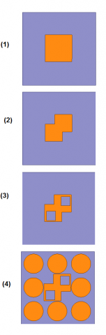
The design procedure is presented in Figure 2.
Figure 2. Design evolution of the antenna
Figure 3 represents the proposed antenna design. The array is consisting of eight numbers of parasitic patches. Parasitic patches are basically used to overcome the limitation of microstrip antenna by increasing the bandwidth. The bandwidth enhancement is achievable by gap coupling, where the parasitic patch is excited through the gap present within it. In this design, circular patches are present with a gap of 9.75mm between the centres of adjacent circles to achieve a wider bandwidth. The parameters of the antenna array are listed in Table 1. The design of the antenna is realized with ANSOFT HFSS.
Figure 3. Geometry of proposed 3X3 array
Table 1. Dimension parameter of proposed antenna
|
Parameter |
Value |
|
Substrate material |
FR4 |
|
Loss tangent |
0.02 |
|
Substrate length (a) |
30mm |
|
Substrate width (a) |
30mm |
|
Substrate thickness |
1.6mm |
|
Centre patch length(L) |
11mm |
|
Centre patch width(W) |
11mm |
|
Radius of parasitic patch(c) |
4mm |
|
Length and width of corner slot(b) |
3.9mm |
|
Length and width of inner slot(d) |
3.8mm |
|
Feed type |
Coaxial feed |
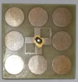
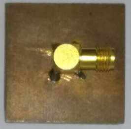
For the verification of the simulation result, one prototype of the antenna array is fabricated. Figure 4 and Figure 5 show the front view and back view of the fabricated antenna.
Figure 4. Front View of proposed array
Figure 5. Back View of proposed array
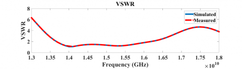
The VSWR of the antenna is represented in Figure 6. For the proper operation of antenna, the VSWR value must lie in the range of 1 to 2. Here the antenna resonates at 14GHz satisfying the standard.
Figure 6. VSWR plot of the proposed array
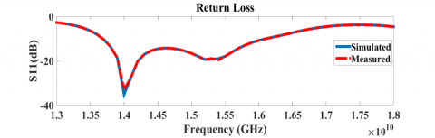
The impedance bandwidth is calculated and is shown in Figure 7. From S11 value we can observe the desired frequency and its relative bandwidth. The measued result agrees with the simulated result. The simulated value results with a return loss of -35dB where as the measured value has a return loss of -33dB. The impedance bandwidth of the array is calculated as 2.4GHz. It is depicted that the measurement value has a good agreement with the predicted value of the simulation.
Figure 7. Impedance bandwidth plot of the proposed array
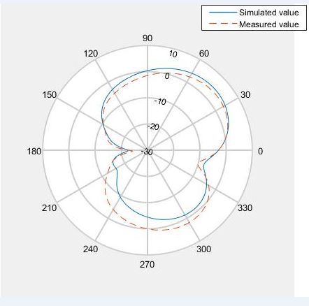
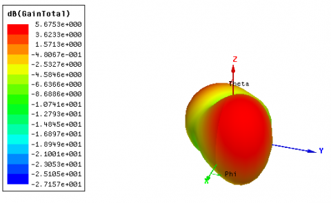
The radiation pattern and the gain of the antenna are shown in Figure 8 and Figure 9. The radiation pattern shows the antenna as omnidirectional. The gain is measured as 5.68 dB. The performance in terms of return loss and bandwidth among the simulated and implemented array antenna is given in Table 2.
The comparison of this proposed array with earlier designs is given in Table 3 for observation and evaluation of the proposed work. The proposed antenna resonates at 14GHz with a wider bandwidth of 2.4GHz and gain of 5.68dB.
Figure 8. Radiation Pattern of proposed array
Figure 9. 3D polar plot of gain of the proposed array
Table 2. Performance analysis of simulated and fabricated antenna
|
Proposed Design |
Return loss (dB) |
Bandwidth (GHz) |
|
Simulated |
-35 |
2.4 |
|
Fabricated |
-33 |
2.4 |
Table 3. Performance analysis
|
Antenna Reference |
Patch Structure |
Resonating Frequency (GHz) |
Bandwidth (GHz) |
Gain(dB) |
|
[16] |
Circular shape |
18 |
2.2 |
10 |
|
[17] |
Circular shape |
4.2 |
0.35 |
12 |
|
[18] |
Circular shape |
2.16 |
0.002 |
4.84 |
|
[22] |
Rectangular shape |
5.43 |
1.04 |
8.22 |
|
[23] |
E shape |
1.3 |
0.514 |
9 |
|
[24] |
EBG structure |
3.58 |
0.072 |
5.8 |
|
[25] |
Rectangular shape |
3.6 |
0.160 |
15.1 |
|
[26] |
Rectangular shape |
5.6 |
0.18 |
5.1 |
|
Proposed Antenna |
Circular shape |
14 |
2.4 |
5.68 |
The paper presents an efficient bandwidth enhancement for the parasitic array. Also, it exhibits a gain of 5.68dB at 14GHz making it convenient for application in Ku band. It has good immunity of signals in case of multipath propagation. To control the antenna’s characteristics there is only one degree of freedom (radius of the patch) for which it is most suitable in wireless communication. The outcome specify that the proposed antenna will perform better in the desired frequency range as compare to other antenna in the same design process.
[1] Mailloux, R., McIlvenna, J., Kernweis, N. (1981). Microstrip array technology. IEEE Transactions on Antennas and Propagation, 29(1): 25-37: http://dx.doi.org/10.1109/TAP.1981.1142525
[2] Garg, R., Bharatia, P., Bhal, I., Ittipiboon, A. (2001). Microstrip Antenna Design Handbook, Norwood, MA: Artech House.
[3] Balanis, C.A. (2007). Antenna Theory Analysis and Design. 2nd Edition, Wiley India (p.) Ltd.
[4] Zavosh, F., Aberle, J.T. (1996). Improving the performance of microstrip-patch antennas. IEEE Antennas and Propagation Magazine, 38(4): 7-12: http://dx.doi.org/10.1109/74.537361
[5] Satrusallya, S., Mohanty, M.N. (2017). Design of an array antenna for 5G wireless network with enhanced bandwidth. In 2017 International Conference on Infocom Technologies and Unmanned Systems (Trends and Future Directions)(ICTUS), pp. 1-5. http://dx.doi.org/10.1109/ICTUS.2017.8286010
[6] Kumar, P., Singh, G. (2012). Gap-coupling: A potential method for enhancing the bandwidth of microstrip antennas. Advanced Computational Techniques in Electromagnetics, 2012: 1-6. http://dx.doi.org/10.5899/2012/acte-00110
[7] Sudeep, B., Goswami, A.K., Yadav, M.V. (2019). Miniaturized dual-band antenna with a rectangular patch and symmetrically placed circles in the partial ground plane. Progress In Electromagnetics Research, 78: 29-37. http://dx.doi.org/10.2528/PIERM18112202
[8] Satrusallya, S., Mohanty, M.N. (2019). Design of optimized microstrip array antenna for wireless communication. In 2019 International Conference on Applied Machine Learning (ICAML), pp. 273-276. http://dx.doi.org/10.1109/ICAML48257.2019.00057
[9] Yu, B., Yang, K., Yang, G. (2017). A novel 28 GHz beam steering array for 5G mobile device with metallic casing application. IEEE Transactions on Antennas and Propagation, 66(1): 462-466. https://doi.org/10.1109/TAP.2017.2772084
[10] Ramli, R.M., Abdul Rahim, S.K., Sabran, M.I., Yong, W.Y., Pon, L.L., Islam, M.T. (2019). Polymer conductive fabric grid array antenna with pliable feature for wearable application. Microwave and Optical Technology Letters, 61(2): 474-478. http://dx.doi.org/10.1002/mop.31585
[11] Farooq, U. (2019). Design and analysis of rectangular microstrip antenna (RMSA) for millimeter wave applications. Journal of Microwave Engineering and Technologies, 6(2): 6-13. http://dx.doi.org/10.18280/ts.360508
[12] Song, Q., Zhang, X.X. (1995). A study on wideband gap-coupled microstrip antenna arrays. IEEE Transactions on Antennas and Propagation, 43(3): 313-317. https://doi.org/10.1109/8.372003
[13] Meshram, M.K., Vishvakarma, B.R. (2001). Gap-coupled microstrip array antenna for wide-band operation. International Journal of Electronics, 88(11): 1161-1175. http://dx.doi.org/10.1080/00207210110071288
[14] Mallahzadeh, A.R., Es' haghi, S., Alipour, A. (2009). Design of an E-shaped MIMO antenna using IWO algorithm for wireless application at 5.8 GHz. Progress In Electromagnetics Research, 90: 187-203. http://dx.doi.org/10.2528/PIER08122704
[15] Ghavami, M. (2002). Wideband smart antenna theory using rectangular array structures. IEEE Transactions on Signal Processing, 50(9): 2143-2151. http://dx.doi.org/10.1109/TSP.2002.801891
[16] Lai, T.F., Mahadi, W.N.L., Soin, N. (2008). Circular patch microstrip array antenna for ku-band. World Academy of Science, Engineering and Technology, 48: 298-302.
[17] Keshtkar, A., Keshtkar, A., Dastkhosh, A.R. (2008). Circular microstrip patch array antenna for C-band altimeter system. International Journal of Antennas and Propagation, 2008: 389418. http://dx.doi.org/10.1155/2008/389418
[18] Dasgupta, S., Gupta, B., Saha, H. (2010). Development of circular microstrip patch antenna array for rectenna application. In 2010 Annual IEEE India Conference (INDICON), pp. 1-6. http://dx.doi.org/10.1109/INDCON.2010.5712719
[19] Kandwal, A., Khah, S.K. (2014). Using parasitic elements for implementing sectoral patch antenna array for wireless applications. International Journal of Microwave and Wireless Technologies, 6(5): 491-496. http://dx.doi.org/10.1017/S1759078713000925
[20] Firmansyah, T., Praptodiyono, S., Aribowo, D., Alam, S., Astuti, D.W., Yunus, M. (2019). Bandwidth enhancement and miniaturization of circular-shaped microstrip antenna based on beleved half-cut structure for MIMO 2×2 application. International Journal of Electrical & Computer Engineering (2088-8708), 9(2). http://dx.doi.org/10.11591/ijece.v9i2.pp1110-1121
[21] Deshmukh, A.A., Ray, K.P. (2015). Proximity fed gap-coupled half E-shaped microstrip antenna array. Sadhana, 40(1): 75-87. http://dx.doi.org/10.1007/s12046-014-0293-y
[22] Abraham, J., Mathew, T., Aanandan, C.K. (2016). A novel proximity fed gap coupled microstrip patch array for wireless applications. Progress In Electromagnetics Research, 61: 171-178. http://dx.doi.org/10.2528/PIERC15111501
[23] Kodgirwar, V.P., Deosarkar, S., Joshi, K. (2020). Design of adaptive array with e-shape slot radiator for smart antenna system. Progress In Electromagnetics Research, 90: 137-146: http://dx.doi.org/10.2528/PIERM19122901
[24] Mohamadzade, B., Lalbakhsh, A., Simorangkir, R. B., Rezaee, A., Hashmi, R.M. (2020). Mutual coupling reduction in microstrip array antenna by employing cut side patches and EBG structures. Progress In Electromagnetics Research, 89: 179-187. http://dx.doi.org/10.2528/PIERM19100703
[25] Jagtap, S., Chaudhari, A., Chaskar, N., Kharche, S., Gupta, R.K. (2018). A wideband microstrip array design using RIS and PRS layers. IEEE Antennas and Wireless Propagation Letters, 17(3): 509-512. http://dx.doi.org/10.1109/LAWP.2018.2799873
[26] Kumar, M., Nath, V. (2016). Analysis of low mutual coupling compact multi-band microstrip patch antenna and its array using defected ground structure. Engineering Science and Technology, an International Journal, 19(2): 866-874. http://dx.doi.org/10.1016/j.jestch.2015.12.003
[27] Pandhare, R.A., Zade, P.L., Abegaonkar, M.P. (2016). Miniaturized microstrip antenna array using defected ground structure with enhanced performance. Engineering Science and Technology, an International Journal, 19(3): 1360-1367. http://dx.doi.org/10.1016/j.jestch.2016.03.007
[28] Salehi, M., Tavakoli, A. (2006). A novel low mutual coupling microstrip antenna array design using defected ground structure. AEU-International Journal of Electronics and Communications, 60(10): 718-723. http://dx.doi.org/10.1016/j.aeue.2005.12.009