Effect of Annealing on the Physical Characteristics of In2O3 Nanoparticle Films

Dhufr Hadi![]() | Hawraa Hadi*
| Hawraa Hadi*![]() | Seham Hassan Salman
| Seham Hassan Salman![]()
© 2025 The authors. This article is published by IIETA and is licensed under the CC BY 4.0 license (http://creativecommons.org/licenses/by/4.0/).
OPEN ACCESS
Indium (III) oxide film was deposited on glass by the thermal evaporation method to study the change in optical and structural characteristics as the annealing temperature varied from 100 to 300℃. The measurement of (XRD) revealed that the prepared and annealed films had a polycrystalline structure. Additionally, the results in terms of grain size and roughness were consistent with the results obtained from studying the surface topography of all films (before and after annealing) using an atomic force microscope (AFM). The optical characteristics also varied with changing annealing temperature, represented by the absorbance, transmittance, and reflectance spectra, and the optical constants, represented by the absorption coefficient, refractive index, and extinction coefficient. The energy gap was found (3.45-3.541) eV.
nanoparticles, indium oxide, thin film, thermal evaporation, annealing, semiconductor
Indium oxide is a chemical compound composed of indium and oxygen elements. It exists in two main forms: indium(I) oxide (In₂O) and Indium (III) oxide (In₂O₃) Indium (I) oxide (In₂O) solid, gray or black opaque crystals, unsolvable in water but dissolves in strong acids, it is uncommon and relatively unstable because it is easily oxidized to In₂O₃ when exposed to air or high temperatures [1, 2].
While indium (III) oxide (In₂O₃) is the more stable and common form, it has properties as it is a yellow to light brown powder, transparent material in the visible range, making it suitable for optoelectronic applications. The electrical conductivity is relatively high in In₂O₃ if it is impure or low in oxygen. The amorphous indium oxide is unsolvable in water but dissolves in strong acids, whereas crystalline indium oxide is unsolvable in both water and acids [2, 3].
Indium oxide (In₂O₃) thin films play a pivotal role in today's and future technology such as (transparent conductive material in displays in Electronic devices, gas sensors and solar cells) due to their smooth and homogeneous surface when prepared using advanced deposition methods, in addition to their high transparency in the visible light range, low infrared absorbance, and good resistance to heat and chemical corrosion [4, 5]. Electrically, Indium Oxide (In₂O₃) is an n-type semiconductor with a wide bandgap energy of 2.7 - 3.7 eV [4, 6].
Due to its thin-film properties, Indium Oxide (In₂O₃) is used in many advanced technological applications, especially in displays, solar cells, and smart electronics. With continuous development, its performance is expected to improve, and its cost will be reduced, making it more widespread in modern industries [7, 8].
Dua’a et al. [9] in their study, concluded that the optical properties of laser-deposited indium oxide/quartz films change depending on the laser power used in deposition, as they found that the energy gap increases with increasing laser power. In the study, Faisal and Salman [10] prepared gas sensors from indium oxide and studied the effect of oxidation time on the membrane's sensitivity to gas, where they found that the sensitivity increased with increasing oxidation time.
Finally in future studies, we propose using indium oxide to manufacture smart, small sensors that can be coupled to smart devices, it can be used on plastic or organic substrates to produce foldable and wearable medical screens and devices and due to its low toxicity, it can be used in biomedicine to manufacture a drug delivery to the target organ.
Thermal oxidation was used to deposit indium oxide nanoparticles on glass substrates with a volume of (2 cm, 2 cm, 400 nm) (length, width, thickness) away from the molybdenum boat about 18 cm. The deposition process was carried out in two stages.
The first stage included the vacuum thermal evaporation of the indium metal on the substrates as mentioned earlier at a deposition rate of about 1.33 ± 0.2 nm per second and under pressure close to 2×10⁵ m bar.
In the second stage, the oxidation reaction of the indium films was carried out as shown in the equation below by using a thermal system with the effect of oxygen present in the system (a flat electric heater to provide heat to the material) for 60 minutes on the sequence at a constant temperature of 350 degrees Celsius.
$2 \operatorname{In}(s)+30=\operatorname{In}_2 O_3$
Indium oxide films were annealed at different temperatures (100,200,300) degrees Celsius for one hour at each temperature.
The change of the crystal structural and crystalline phases of the prepared and annealed films vs change in annealing temperature was studied using an X-ray diffraction device (XRD-6000, Cu, Kα and wavelength = 1.5406 A) manufactured by the Japanese company Shimadzu.
While the optical characteristics of the thin films and the extent of the effect of annealing on them, the absorbance and transmittance of all prepared and annealed films were measured using UV-visible 1800 spectroscopy over a wide range of wavelengths.
3.1 The X-ray diffraction (XRD) measurement
The X-ray diffraction pattern in Figure 1 shows several peaks, all of which are related to indium oxide. This indicates that the prepared thin films' crystal structure is polycrystalline of the cubic type and the prevailing orientation before annealing (222). After one hour of annealing, the films exhibited enhanced stability along the dominant crystallographic direction (321), while the intensity of peaks corresponding to other crystallographic directions diminished. The rise in intensity for this direction with increasing annealing temperature suggests the presence of certain preferred levels for crystal growth. As a result, the intensity of this peak increases, indicating that the film structure has improved crystallization. In other words, annealing at high temperatures enhances the degree of crystallization of the film material and reduces crystal defects, these changes directly affect the physical and chemical properties of the film, and thus its performance in various applications, as the crystal orientation affects the arrangement of atoms and electronic paths within the crystal, leading to an increase or decrease in electrical conductivity. As for the optical properties, the transparency value in the visible range and the width of the optical energy gap change slightly depending on the orientation. Changing the crystal to the 321 orientation leads to a change in light absorption or scattering, which is a crucial factor in solar cells and displays. The film's surface becomes rougher when the crystal orientation changes to the 321 direction, leading to improved sensitivity of some gases in gas sensors, which is consistent with the results reported in previous studies [8, 11].
Figure 1. The X-ray diffraction
When comparing the pattern obtained from X-ray diffraction, including the surface area (dhkl), the diffraction angles (2θ), and the lattice parameter at the locations of the distinctive peaks of the prepared film models, we find that the results are identical to the values stated in the standard card of the American Institute for Materials Testing. This is illustrated in Table 1.
Table 1. The parameters of interest obtained from X-ray diffraction for (In2O3), which annealed at different temperatures
|
Annealing T (c) |
Position (2ϴ) |
d Spacing (Ao) |
Orientation (hkl) |
FWHM (Deg) |
Crystallite Size (nm) |
Lattice Parameter (Ao) |
|
un annealing |
30.5 |
2.9203 |
222 |
0.763 |
11.27 |
10.12 |
|
100 |
33.0964 |
2.7045 |
132 |
0.634 |
13.65 |
10.12 |
|
200 |
33.0194 |
2.7106 |
132 |
0.629 |
13.75 |
10.14 |
|
300 |
33.0194 |
2.7106 |
132 |
0.629 |
13.75 |
10.14 |
We obtain structural parameters such as strain, crystalline size C.S, dislocation density d and number of crystallites per area are calculated by using the following equations. respectively [12-15] and listed in Table 2 and influence of increase annealing temp. on the structural parameters.
Table 2. XRD results for (In2O3) films
|
Annealing T (c) |
Position (2ϴ) |
Crystallite Size (nm) |
ɛ |
δ |
N |
|
un annealing |
30.5 |
11.27 |
0.003212 |
0.007871 |
0.279323 |
|
100 |
33.0964 |
13.65 |
0.002652 |
0.005364 |
0.157141 |
|
200 |
33.0194 |
13.75 |
0.002631 |
0.005283 |
0.15358 |
|
300 |
33.0194 |
13.75 |
0.002631 |
0.005283 |
0.15358 |
$\varepsilon=\beta \operatorname{Cos} \theta / 4$ (1)
C. $S=0.94 \lambda / \beta \operatorname{Cos} \theta$ (2)
$\delta=1 /(\mathrm{C} . \mathrm{S}) 2$ (3)
$\mathrm{N}=\mathrm{t} /(\mathrm{C} . \mathrm{S}) 3$ (4)
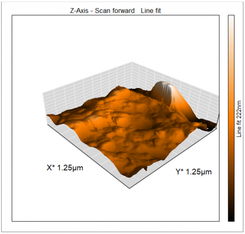
3.2 AFM measurements
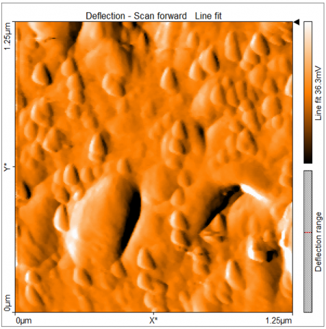
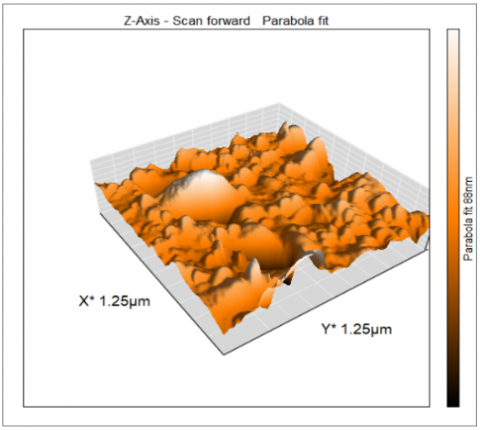
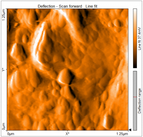
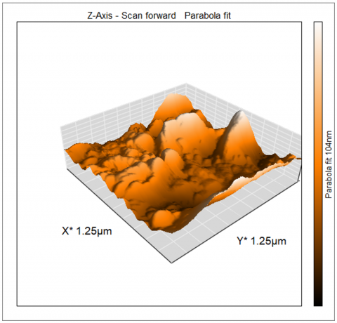
Atomic force microscopy (AFM) surface morphology study provides a two-dimensional and three-dimensional view of the grain arrangement. It provides accurate statistical values regarding the average grain size, distribution, and surface roughness, including essential information based on the square root of the average surface roughness. Figure 2 shows the AFM image at different annealing temperatures. It is observed that the film exhibits better uniformity and crystal structure after annealing. RMSE and R values of the surface roughness and grain size are detailed in Table 3. Notably, annealing results in increased surface roughness, indicating a rise in grain size and a reduction in grain boundaries. These findings are consistent with the results obtained from X-ray diffraction analysis.
|
un-annealing |
||
|
100℃ |
||
|
200℃ |
||
|
300℃ |
Figure 2. Atomic force microscopy (AFM) surface morphology
Table 3. The parameters of interest obtained from AFM for (In2O3) which annealed at different temperatures
|
Annealing T (c) |
RMSE (nm) |
Average Roughness (R) (nm) |
Grain Size |
|
un annealing |
6.16 |
4.85 |
22.96 |
|
100 |
10.654 |
7.2227 |
54.018 |
|
200 |
16.105 |
12.584 |
58.015 |
|
300 |
32.5 |
22.628 |
147.85 |
3.3 Optical properties
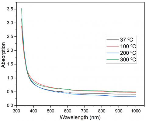
Figure 3 illustrates the absorbance and transmittance spectra in the range of 300 to 1100 nm. For all prepared and annealed films, the absorbance peaks at shorter wavelengths and decreases as the wavelength increases. While the transmittance spectrum behaves inversely to the absorbance spectrum, Figure 3 illustrates that transmittance begins at the wavelength that represents the boundary between the absorbance and transmittance of the thin film material, or the so-called cutoff wavelength. Transmittance then generally increases with increasing wavelength of electromagnetic radiation incident on the thin film, i.e., at wavelengths with lower energies.
This behavior in the absorbance and transmittance spectrum occurs because the energy of the incident photons is less than the optical energy gap, which prevents the excitation.
Observing Figure 3, we can see that the absorbance increases and transmittance decreases at annealing temperatures of 100℃ and 300℃, this suggests that annealing at 100°C and 300°C generates local energy levels between the valence band and the conduction band, which facilitate the transfer of electrons from the valence band to the conduction band. In contrast, the absorbance decreases and transmittance increases at annealing temperatures of 200℃, indicating that this temperature results in the removal of structural defect levels associated with the preparation process and a reduction in the local energy levels.
Figure 3. Illustrates the absorbance and transmittance spectra
Reflectivity (R) was calculated from the absorbance and transmittance spectra using the law of conservation of energy and according to Eq. (5) [16]. Figure 4 shows that reflectivity increases with increasing wavelength for short wavelengths, while for long wavelengths, it decreases with increasing wavelength.
$A+R+T=1$ (5)
Figure 4 notes the effect of annealing on the films' reflectivity. Where films annealed at temperatures 100 and 300℃ increased their reflectivity.
Figure 4. Reflectivity of In2O3 films
In contrast, films annealed at temperature 200℃ decreased their reflectivity compared to the reflectivity of films prior to annealing. It is important to note that reflectivity is largely influenced by the morphology of films surface.
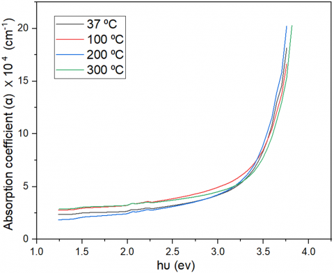
$\alpha=2.303 \frac{\mathrm{~A}}{\mathrm{t}}$ (6)
Figure 5 shows the change in $(\alpha)$ for annealed and unannealed indium oxide films which is calculated from Eq. (6) [17]. It is low at low photon energies, where the probability of electronic transitions is low. However, as the photon energy increases, the absorption coefficient rises significantly, exceeding a value of 104. This increase indicates the occurrence of direct electronic transitions.
Figure 5. The absorption coefficient
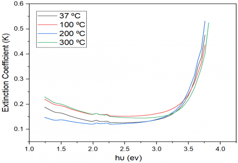
Figure 6 shows the extinction coefficient (k) for annealed and unannealed indium oxide films which is calculated from Eq. (7) [18].
$k=\frac{\alpha \lambda}{4 \pi}$ (7)
Figure 6. The extinction coefficient
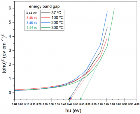
By using the Tauc model according to the Eq. (8) [19, 20] calculated the optical energy bandgap for the allowed direct electronic transitions of indium oxide thin films.
$\alpha h v=P\left(h v-E_g\right)^r$ (8)
where, the value of (r=1/2), by drawing the linear relationship between (αhv) and the incident photon energy (hv) and taking the straight line extension from the curve (fitting) to intersect the photon energy axis at the point (αhv) = 0, which represents the value of the optical energy gap for the allowed direct transition, and its values ranged between (3.44-3.54) eV as shown in Figure 7, these results are consistent with research [8, 10].
Figure 7. Shows the optical energy gap
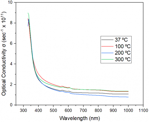
Figure 8 shows the optical conductivity is calculated from the following relationship (9) [19].
$\sigma_{\mathrm{op}}=\alpha \mathrm{nc} / 4 \pi$ (9)
Figure 8. The optical conductivity
In2O3 thin films was prepared by vacuum thermal evaporation on glass substrate at R.T and these films to annealing at 100, 200 and 300℃. The annealing temperature changes the various properties of the In2O3 thin films. The crystallite size of films annealed increased with increase annealed temp and change orientation of crystalline planes from 222 to 132 plane, the absorbance increases and transmittance decreases at annealing temperatures of 100℃ and 300℃, the optical energy gap for the allowed direct transition, and its values ranged between 3.44-3.54 eV.
The author gratefully acknowledges the support and facilities provided by the Department of Anesthesia, College of Health and Medical Techniques/Kufa, Al-Furat Al-Awsat Technical University, Al-Kufa, Iraq. The academic environment and resources made available by the university were essential in the successful completion of this research.
[1] Hasan, B.A., Rzaij, J.M., Ali, I.M. (2016). Sensing properties of (In₂O₃: Eu) thin films. Australian Journal of Basic and Applied Sciences, 10(8): 143-150. https://www.researchgate.net/publication/325131186.
[2] Fakhri, M.A. (2014). Effect of substrate temperature on optical and structural properties of indium oxide thin films prepared by reactive PLD method. Engineering and Technology Journal, 32(5): 1323-1330.
[3] Sudha, A., Sharma, S.L., Maity, T.K. (2015). Effects of annealing temperature on structural and electrical properties of indium oxide thin films prepared by thermal evaporation. Materials Letters, 157: 19-22. https://doi.org/10.1016/j.matlet.2015.05.050
[4] Kareem, M.A., Rasheed, R.T., Al-Algawi, S.D., Jaffer, L.A. (2016). Solvothermal synthesis and characterization of indium oxid nanoparticles. Iraqi Journal of Science, 57: 2880-2890.
[5] Mohammed, D.A., Jawad, M. (2018). Studying the effect of annealing temperature on some physical properties of In₂O₃ thin films. Engineering and Technology Journal, 36(2 Part B): 124-127. https://doi.org/10.30684/etj.36.2B.5
[6] Suthar, D., Dhaka, M.S. (2023). Physical properties of thermal annealing induced In2O3 thin films for sensing layer applications. Materials Today: Proceedings. https://doi.org/10.1016/j.matpr.2023.06.392
[7] Xiao, N., Yuvaraja, S., Chettri, D., Liu, Z., Lu, Y., Liao, C., Tang, X., Li, X. (2023). The influence of annealing atmosphere on sputtered indium oxide thin-film transistors. Journal of Physics D: Applied Physics, 56(42): 425102. https://doi.org/10.1088/1361-6463/ace6b8
[8] Hussain, S.A., Al-Hilo, E.A., Hatem, A.H. (2016). Influence of annealing on the structural and optical characteristics of indium oxide thin films prepared using thermal evaporation in a vacuum method. Journal of Advances in Physics, 12(4): 4415-4421.
[9] Dua’a, R.T., Alwahib, A.A., Fakhri, M.A., Qaeed, M.A., Gopinath, S.C. (2024). Optical investigation of In2O3/quartz nano-films deposited at different laser energies. International Journal of Nanoelectronics and Materials (IJNeaM), 17: 169-174. https://doi.org/10.58915/ijneam.v17iJune.851
[10] Faisal, M.H., Salman, S.H. (2024). Effect of oxidation times on Gas sensitivity and characterization for (In2O3) thin films produced by thermal evaporated. In Journal of Physics: Conference Series, Metz, France, p. 012010. https://doi.org/10.1088/1742-6596/2857/1/012010
[11] Veeraswamy, Y., Vijayakumr, Y., Reddy, M.R. (2013). Structural and optical characterization of indium oxide thin films by vacuum thermal evaporation. In International Conference on Advanced Nanomaterials & Emerging Engineering Technologies, Chennai, India, pp. 502-505. https://doi.org/10.1109/ICANMEET.2013.6609348
[12] Abbas, I.A., Hazaa, S.Q., Salman, S.H. (2021). Employment of titanium dioxide thin film on NO2 gas sensing. In Journal of Physics: Conference Series, Baghdad, Iraq, p. 032061. https://doi.org/10.1088/1742-6596/1879/3/032061
[13] Salman, S.H., Hassan, N.A., Ahmed, G.S. (2022). Copper telluride thin films for gas sensing applications. Chalcogenide Letters, 19(2): 125-130. https://doi.org/10.15251/CL.2022.192.125
[14] Shehab, A.A., Salman, S.H. (2017). Effect annealing temperatures on the structural properties of ZnO thin films prepared by chemical bath deposition. Ibn AL-Haitham Journal For Pure and Applied Science, 25(1): 1-8.
[15] Alrazak, A.H.A., Salman, S.H., Abbas, I.A., Mustafa, M.H., Ali, H.M., Abbas, S.A. (2025). Influence of doping with silver nanoparticles on the molybdenum trioxide gas sensor prepared by spray pyrolysis. Digest Journal of Nanomaterials & Biostructures (DJNB), 20(1): 191-199. https://doi.org/10.15251/DJNB.2025.201.191
[16] Ibrahim, H.K., Salem, R.D. (2012). Optical properties of poly vinyl alcohol (PVA) doped with Ali Zarin Orange Azo Dye thin films prepared by cast method. Journal of Kufa-Physics, 4(1): 11-21.
[17] Hadi, H., Mohammed, K.A., Hadi, D. (2022). Some physical properties of pure and Cu, Fe-doped CdS thin films. International Journal of Nanoscience, 21(4): 2250031. https://doi.org/10.1142/S0219581X22500314
[18] Salman, S.H., Abbas, E.A., Abbas, S.A. (2016). Effect of Gamma irradiation on the optical properties of (PVA: CuCl2) films. Iraqi Journal of Science, 57(3B): 1968-1974.
[19] Ahmed, G.S., Salman, S.H., Abid, E.Y. (2016). Study the optical properties of polymer poly vinyl alcohol doped with CuO and Fe2Cl3 thin films. Ibn AL-Haitham Journal For Pure and Applied Sciences, 29(3): 345-354.
[20] Salman, S.H., Ali, S.M., Ahmed, G.S. (2021). Study the effect of annealing on structural and optical properties of indium selenide (InSe) thin films prepared by vacuum thermal evaporation technique. In Journal of Physics: Conference Series, Baghdad, Iraq, p. 032058. https://doi.org/10.1088/1742-6596/1879/3/032058