Ghazwan Ghazi Ali*![]() | Mohammed Ibrahim Ismael
| Mohammed Ibrahim Ismael![]() | Taghreed Mahmood Younus
| Taghreed Mahmood Younus![]()
© 2025 The authors. This article is published by IIETA and is licensed under the CC BY 4.0 license (http://creativecommons.org/licenses/by/4.0/).
OPEN ACCESS
This work develops the performance of porous silicon photodetector. Magnesium oxide (MgO) nanostructure was deposited on porous silicon substrates by chemical spray method at concentration 0.1M. We have investigated the influence of etching time on the structural, morphological optical and electrical properties. XRD study exhibited that the fresh porous silicon and MgO/PSi samples were polycrystalline in nature of cubic structure (fcc). Porous silicon has inhomogeneous arrangement of the pores with some voids separated between walls on the surface. The nucleation growth of MgO thin film increased and completely covering within the pores. the Raman peaks of the MgO/PSi were shifted to the red position with increasing etching time. I–V characteristics of the MgO/PSi exhibit Schottky diode behavior of all samples. Apart of this, the photodetectors values of all samples raise slighty with etching time. Additionally, The optimum value of quantum efficiency for MgO/PSi were found to be 59% and 32% at wavelength 300-400nm and drops values to 8% and 6%, at the near infrared range respectively. The efficiency of MgO/PSi improved with increasing etching time. The performance of the prepared films depends on fabrication conditions.
MgO, porous silicon, XRD, Raman scattering, photodetector
Magnesium element (Mg) belongs to Group II, and oxygen (O), the second element, belongs to Group VI. The crystal structure of magnesium oxide (MgO) is face-center cubic (fcc), similar to that of the NaCl crystal structure [1, 2]. It has unique physical and chemical properties, such as magnetic and optical characteristics. It has numerous features such as good mechanical strength and heat resistance [3]. Furthermore, it has high optical transparency and boreding band gap of 3.4–6.8 eV, hardness, high point melting, low electrical and thermal conductivity as well as small electron affinity [4]. MgO is non-toxicity and environmental friendly, as well as it has chemical and physical stability [5]. Recently, magnesium oxide (MgO) has more attracted attention by many researchers due to its used several applications such as gas sensor, photodetector, photovoltaic, photonic, photocatalytic, capacitors, antibacterial, refractory materials and electro-optical devices [6, 7]. Several methods have been used to deposit of MgO thin film such as chemical spray technique, chemical vapor deposition (CVD), plasma enhanced vapor deposition (PECVD), sol-gel, sputtering and laser evaporation method [8, 9]. The spray technique is the easy method and it has a low cost and is not time-consuming [10]. Porous silicon has large surface area around (107 times larger than that of bulk) and a wide spectral range in room temperature [11]. Porous silicon can be utilized in different fields such as filters, solar cell, switching, photovoltaic devices, waveguides, chemical sensors, biological sensors and light emitting diode [12-14]. The surface structure of PSi has spider network of pores separated by thin walls with nano-size of Si substrate [15]. Four techniques can be used to form prepartion substrate for example anodization deposition, photo-electrochemical analysis, photo-chemical method and ultasonic method [16]. The photo-electrochemical method is regarded one the simplest techniques to prepare porous silicon thin film. It is low cost and environmental friendly [17]. This method can be achieved to obtain high efficiency and homogenously of deposited thin films by controlling parameters such as fixed current, periodic time and HF solution in order to obtain the porosity and uniform thickness [18]. Based on previous papers, the combination of high-quality MgO nanostructure and porous silicon substrate are a good matching deposition especially corresponding with lattice constants and optoelectronic devices [19]. In addition, the heterojunction of MgO/PSi thin film can be enhanced the performance of response and efficiency of photodetector. Maher et al. (2021) characterized and studied of magnesium oxide (MgO) thin films with different concentrations by chemical spray method, they exhibt the structural, optical and morphological properties of MgO thin films. They investegated that the reflective surface will prevent an increase in surface temperature, which could be beneficial in optoelectronic applications [20]. Mhetre et al. [21] prepared MgO thin films by spray pyrolysis method. They exhibit the nanocomposites of MgO have high chemical stability and photodetector devices. The goal of this manuscript is to study the structural, chemical, electrical and optical charactristics of MgO/PS nanostructure of various etching time in order to obtain high performance photodetector.
2.1 Characterization of devices
X-ray diffraction measurements were achieved using Cu Kα source (D5-advance / Bruker) with wavelength λ=1.54528 Å, the data of the diffraction angle was investigated from 20± to 100± at speed of 0:04±per second. The surface and the cross-section morphology were achieved by characterization a cold field scanning electron microscope (FESEM) (JEUB-JAM-6251E) and operated up to voltage 10 keV. Furthermore, Energy dispersive scattering (EDS) was recorded using the advice (JeoA; JAS-7131LV). Raman spectroscopy was characterized using (GN SER No. 82140) made in (Germany). The laser helium-neon was used as a beam source of the back scattered light intensity within several time. Optical transmission and absorption measurements were investigated using an CBAD AQ-4118 optical spectrum analyzer by the spectral range (300–1000 nm). The current-voltage (I-V) characterization were achieved using digital multimeter, dual farnel ET 31/2 power supply were used. The Aluminum (Al) contact as electrode with porous silicon layer was used. The parameters of photodetector measurements were carried out using Monochromatic light source as tungsten–halogen lamp with Light intensity(38.2 mW/cm2) and wavelength (200-100nm).
2.2 Formation mechanism details of porous silicon
Crystalline silicon wafer of n-type (111) with a resistivity of (1-10 ohm. cm) and thickness (500+25µm) were prepared using photo-electrochemical etching method. This method is easy achievement compared to other methods.The parameter conditions were used such as the current density(10mA/cm2), hydrofluoric acid (18% HF), ethanol (99% C2H5OH) and various etching time (5, 10, 15min). The setup of photo-electrochemical anodized cell was made of Teflon and consist of tungsten source (100W/cm2), power supply, digital multimeter. Furthermore, two electrodes were connected in electrical circuit, the first one as cathode electrode made of gold and the second part as anode electrode made of stainless-steel as the Figure 1(a). The process was carried out at 10 mA cm2 and different etching time at 5, 10, 15min respectively.
2.3 Preparation of magnesium oxide nanostructure
Initially, MgO thin films were prepared of reaction solution using magnesium chloride MgCl2. 5H2O that was dissolved in deionized water (40ml) and NaOH (40ml) at concentration 0.1M and 80℃ reaction temperature as stabilizer as following Eq. (1) [22]:
$\begin{gathered}4 \mathrm{NaOH}(a q)+\mathrm{MgCl}_2 .5 \mathrm{H}_2 \mathrm{O}(a q) \rightarrow \mathrm{MgO}(\mathrm{s})+4 \mathrm{NaCl} \\ (a q)+7 \mathrm{H}_2 \mathrm{O}\end{gathered}$ (1)
The magnesium oxide solution was heated at 85℃ using magnetic stirring at 2hr. In the first time the solution looks like light white color and change to dark white color after 90min. The thin films were deposited on the glass substrates using chemical spray pyrolysis at tempreture 260℃ and 7.0 atmospheric pressure with several spray number at 12, 14 and 16. Beside, the time was fixed at 6 seconds as illustrated the Figure 1(b). In addition to this, the deposited thickness could be estimated using the following equation procedure:
$t=\frac{m_2 m_1}{\rho \mathrm{~A}}$ (2)
The surface thickness refers to $t$ and $m_2-m_1$ symbolizes the weight samples, the density indicats to $\rho$ of MgO (3.58 $\mathrm{gm} / \mathrm{cm}^3$). Furthermore, the prepared thickness depend on fabrication parameters.
Figure 1. Set up of work diagram (a) cell of porous silicon Fabrication, (b) Spray pyrolysis method
3.1 X-ray diffraction of MgO/porous silicon
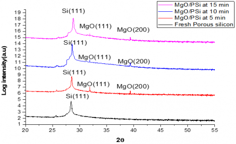
Figure 2 exhibits X-ray diffraction patterns of MgO thin film on porous silicon substrates. All samples have cubic polycrystalline crystal structure. In detail, the strong peak appears at orientation (111) corresponded to 2θ=28.64 belongs to crystalline silicon substrate. Clearly, new peaks appear of XRD patterns related to MgO thin films at 2θ=31.90o and 39.33o corresponded to (111) and (200) respectively (JCPDS No: 00-045-0946) [19]. The grain size (D) of MgO/PSi can be determined by Sherrer formula [23]:
$\mathrm{D}=\frac{k \lambda}{R \cos \theta}$ (3)
where, $B$ refers to full with half maximum, $k$ indicates to the constant 0.9 and $\lambda$ symbolizes $(0.1543 \mathrm{~nm})$ as Table 1.
Figure 2. X-Ray diffraction pattern for (a) Fresh porous silicon at etching time 5min, (b) MgO/PSi at etching time 5min, (c) MgO/PSi at etching time 10min, (d) MgO/PSi at etching time 15min
Besides, the diffraction angle of all deposited thin films perhaps converted to the low account angle due to expanded in lattice constant with increasing etching time. The grian size decresese with increasing FWHM. Our results are good agreements with previous work [24]. The lattice constant a of the MgO thin films can be estimated by the relation [25]:
$a(\mathrm{hkl})=\mathrm{dhkl} \sqrt{h^2}+k^2+l^2$ (4)
The lattic constant of MgO thin film was found to be 4.2Ao.
Table 1. Data of crystallites size, distance between planes, FWHM, of MgO/PSi with different etching time (5, 10 and 15min)
|
Sample |
Etching Time (min) |
d (Ao) |
FWHM (deg) |
D (nm) |
|
Pure porous silicon |
5 |
3.261 |
0.4183 |
0.83017 |
|
MgO/Porous silicon |
5 |
2.712 |
0.8256 |
0.6217 |
|
1.316 |
1.4357 |
0.4252 |
||
|
1.4263 |
0.5904 |
0.6129 |
||
|
MgO/Porous silicon |
10 |
1.8514 |
1.1752 |
0.5168 |
|
1.265 |
1.6291 |
0.3481 |
||
|
1.359 |
3.998 |
0.3831 |
||
|
MgO/Porous silicon |
15 |
1.162 |
1.3283 |
0.7192 |
|
1.177 |
1.8152 |
0.2161 |
||
|
1.2865 |
0.0828 |
0.2856 |
3.2 High-resolution scanning electron microscope (FESEM)
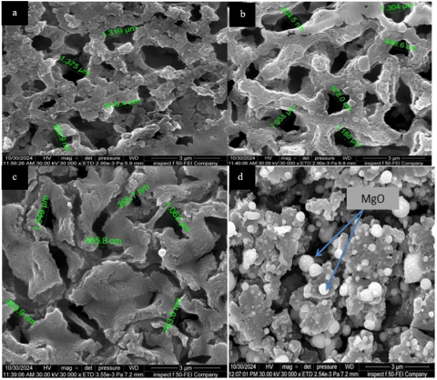
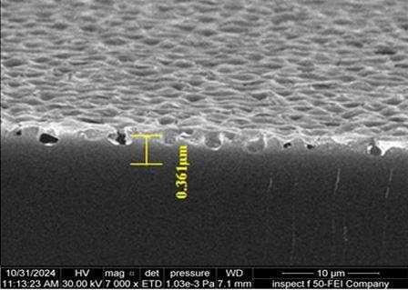
Figures 3 and 4 exhibit the surface morphology (FESEM) images of the MgO/porous silicon thin films at different etching time 5, 10 and 15min. As can be seen, the porous silicon has inhomogeneous arrangement of the pores with some voids separated between walls on the surface as Figure 3(a). In detail, the pore size becomes larger after increasing etching time due to the dissolution of electrochemical of surface during the process. Increasing of etching time leads to the formation of defects. Various defects created by the localization of ions vacancies. These defects are play important role in the microstructure of a material. as Figure 3(b). Clearly, the nucleation growth of MgO thin film increased and completely covering within the pores [26]. The MgO nanostructure are good distribution and homogeneous on denser surface also the presence some spherical particles and agglomerated chains [27]. The particle size of the MgO thin films was found to be 355–763 nm as Figure 3(c) and (d). The cross section of MgO/PSi revealed presence of some islands aggregated, the thickness of deposited film was found to be (361nm) at etching time 5min as Figure 4. It should be noted here that the surface thickness of the deposited films can be used as the previously Eq. (2). Obviously, the thickness of MgO thin film increases with increment number of sprays (10, 15 and 20) due to aggregations and interface band transition at localized states at the surface.
Figure 3. FESEM of top surface (a) fresh porous silicon at etching time 5min, (b) fresh porous silicon at etching time 15min, (c) MgO/PSi at etching time 5min, (d) MgO/PSi at etching time 15min
Figure 4. FESEM of cross section of MgO/PSi at etching time 5min
3.3 EDX
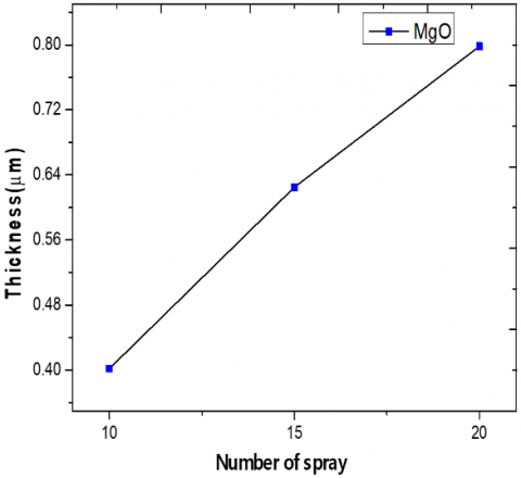
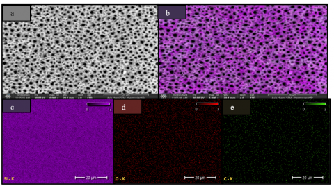
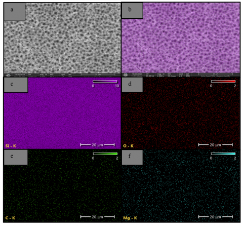
The stoichiometric analysis (EDX) of MgO/PSi nanostructure was observed at etching time (5, 10 and 15min). It is clear, the presence of Si, O and C elements during preparation process, the magnesium oxide nanostructure are good distribution and homogeneously at the surface. The analysis confirms the highly performance of the deposited thin films. It can be seen, the weight ratio of the Si atoms was increased with increasing etching time due to dissolve of pores and leading to increasing number of pores at the surface as Figures 5-13. And the effect of varying the number of sprays on the deposited film thickness is summarized in Table 2, which shows an increase in thickness with more sprays.
Figure 5. Relationship between thickness and number of spray of MgO deposited on glass substrate
Figure 6. Mapping color of EDX analysis of Si, O and C elements at etching 5min
Figure 7. EDX analysis and table of pre-porous silicon at etching time 5min
Figure 8. Mapping color of EDX analysis of Si, O and C elements at etching 15min
Figure 9. EDX analysis and table of pre-porous silicon at etching time 15min
Figure 10. Mapping color of EDX analysis of Si, O, C and Mg elements at etching 5min
Figure 11. EDX analysis and table of MgO/ porous silicon at etching time 5min
Figure 12. Mapping color of EDX analysis of Si, O, and Mg elements at etching 15min
Figure 13. EDX analysis and table of MgO/ porous silicon at etching time 15min
Table 2. Parameters of weight, thickness and number of spray (10, 15 and 20)
|
Number of Spray |
Weight (gm) |
Thickness (µm) |
|
10 |
0.0009 |
0.402 |
|
20 |
0.0014 |
0.625 |
|
30 |
0.0018 |
0.798 |
3.4 Raman scattering
The Raman analysis of the fresh porous silicon and MgO/porous silicon samples at different etching time (5, 10 and 15min) was observed in Figure 14 and Table 3. It can be seen that all peaks of the prepared samples in Raman spectra confirm that the silicon structure remains crystallinity phase before and after deposition. Furthermore, the peak position of the Raman spectrum of the fresh porous silicon was found to be 1.52 cm-1. Currently, the peaks of the MgO/PSi were slightly shifted to the red position (lower wave numbers) with increasing etching time and can be found 4.6 cm-1, 9.3 cm-1 and 14.2 cm-1 at 5, 10 and 15min respectively. The results indicate that the intensity of the peaks increases after doping of MgO due to interaction of phone scattering with the vibration mode of samples. The Raman scattering of the MgO/PSi nanostructures was modified, which is depends on preparation conditions such as etching time, current density and acid solution (HF) [28].
Figure 14. Raman scattering of MgO/PSi at etching time (5, 10 and 15min)
Table 3. Raman parameters of the porous silicon before and after deposition of MgO thin film
|
Sample |
Etching Time (min) |
Wave Number (cm-1) |
FWHM (deg.) |
Intensity (a.u.) |
|
Fresh porous silicon |
5 |
513.129 |
97.623 |
1.52 |
|
MgO/PSi |
5 |
510.552 |
105.17181 |
4.6 |
|
MgO/PSi |
10 |
507.975 |
109.19373 |
9.3 |
|
MgO/PSi |
15 |
506.465 |
114.673 |
14.2 |
3.5 FTIR analysis
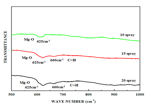
Figure 15 exhibts the stoichiometric analysis spectra (FTIR) of the nanostructure thin film at concentrations 0.1M in the range of 500 –1000 cm–1 using number of spray. It can be seen the strong absorption peak can be observed at 625 cm–1. This may be indicated to vibrational mode of the longitudinal optical phonon modes (LO) of MgO lattice structure. Additionally, the stretching modes of C=H groups are shown at 660 cm–1. Our results are suitable agreement with previous papers [29].
Figure 15. FTIR of MgO/PSi at etching time (5, 10 and 15min)
3.6 UV-Spectrophotometer
The optical analysis of the MgO thin films was investigated using (UV-Vis Spectrophotometer) of wavelength 300–1000 nm. Also, the concentration value to prepare the deposited film is (0.2M) as well as the number of steps at (10, 20, 30). The results indicate that the absorbance curves were observed as Figure 16(a). It should be noted, the absorbance value reduces with raise of wavelength. In addition, the absorption curves of the MgO thin films decrease sharply after λ=360 nm of all samples. The results indicate that the absorption spectra of MgO increase with increasing number of spray. This could be due to the defects accumulation with the number of spraying, this defects may be caused to appere the additioal energy levels and lead to modifier the optical properties of materials and can be used the electronic devices [30]. Figure16(b) shows the transmission spectra of (MgO) thin films as a function of the wavelength. It can be seen, the deposited films have high transmittance values about 95% in the visible region. The transmission spectra decrease with increasing number of spraying due to the optical losses in the visible range could be ascribed to the scattering of light on the surface [31]. Figure 16(c) represents the absorption coefficient (α) of MgO thin films, which can be used by the following Eq. (5):
$\alpha=2.33 \frac{{A}}{{t}}$ (5)
The surface thickness refers to (t). The results indecate that the absorption coefficient as a function of wavelength decreases with increasing of wavelength, also the absorption coefficient increases with the steps of spraying. The high value of the absorption coefficient of MgO thin films ($\alpha \geq 10^4 \mathrm{~cm}^{-1}$) symbolize to the additional energy levels [32]. Figure 16(d) indicates the relationship between $(\alpha\,\, \mathrm{h} v)^2$, photon energy (hv) of MgO films. The calculation of energy gap by the following Eq. (6):
$\alpha \mathrm{h} v=\beta(\mathrm{h} v-\mathrm{Eg})^{\mathrm{c}}$ (6)
The equation parameters refer to the fixed value ($\beta$), the absorption coefficient refers to α and c indicates to (direct transition or indirect transition). The energy gap values decrease with increasing number of spraying, this is due to overlap energy levels, this is created number of oxygen voids generated by the n-type MgO. The energy gap was found to be 4, 3.95, 3.85 eV at number of steps (10, 20, 30). This is a good results and agreement with previouly published papers [33].
Figure 16. Spectra of UV visible MgO Thin films (a) Absorbance, (b) Transmittance, (c) Absorption coefficient, (d) Evaluation of energy gap
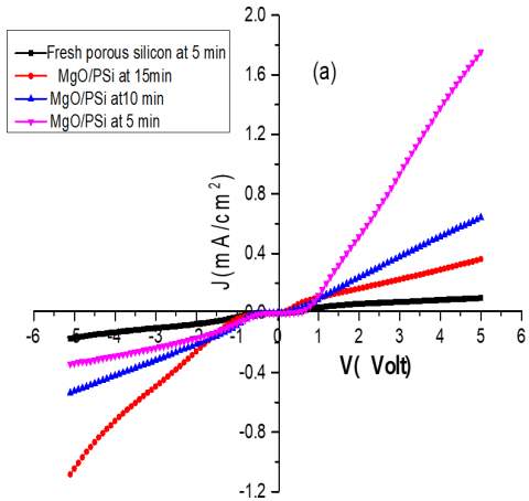
3.7 I-V measurements
I–V charactristics of MgO/PS samples at different etching time were observed in Figure 17. In details, the current-voltage curves confirm Schottky diode behavior of all samples. It can be noted, the forward-bias current values increase with increasing applied voltage [34]. Clearly, the curves of this figure are depended on the priodic time values. Furthermore, the output current decreases with raises time value due to increase number of pores during the preparation process which is affected on the conductivity of the device as Figure 17(a). The formation of the pore walls may be affected on the resistance of samples. In addition, the interference between porous silicon and crystalline silicon substrate is one of the key role parameter which acts as the capture states that degrade semiconductor device performance. Figure 17(b) exhibits I-V characteristics under illumination, the excess of number of generated photo carriers were observed due to increase of minority carriers at the surface. The effect of illumination factor leads to increase reverse current-voltage parameters [35]. The resistivity of the PSi can be evaluated by the following formula:
$\rho_{P S i}=\frac{d V}{d J \cdot d p s i}$ (7)
where, $\mathrm{dV} / \mathrm{dJ}$ refers to the slope at the ohmic part of currentvoltage characteristic, $\rho_{\text {PSi }}$ symbolizes to resistivity value and d is the PSi thickness. Besides, the following formula may be estimated the ideality factor and the barrier height:
$n=\frac{q}{K T}\left[\frac{d(L n I)}{d V}\right]^{-1}$ (8)
$\Phi_B=\frac{k_B T}{q} \operatorname{In}\left(\frac{A^{* *} T^2}{J}\right)$ (9)
where, $\left[\frac{d(L n I)}{d V}\right]^{-1}$ represents the ohmic part, J is the current. Table 4 observed the parameters of the $\mathrm{MgO} / \mathrm{PSi}$ nanostructures.
Figure 17. I-V properties of MgO/PS of etching time 5, 10, 15min (a) at the dark, (b) under illumination
Table 4. Parameters of resistivity, height of barrier, ideality factor and saturation current at periodic time 5, 10, 15 min for MgO/PS device
|
Sample |
Etching time(min) |
Js (mA/cm2) |
N |
$\varphi B$ (eV) |
(Ω.cm) $\rho$ |
|
Fresh porous silicon |
15 |
8.41 |
2.87 |
0.78 |
5.7×10⁷ |
|
MgO/Psi |
5 |
32.65 |
2.24 |
0.632 |
1.63×10⁵ |
|
MgO/Psi |
10 |
18.25 |
2.32 |
0.652 |
3.52×10⁶ |
|
MgO/Psi |
15 |
12.76 |
2.72 |
0.71 |
8.52×10⁶ |
3.8 Photodetector
Spectral responsivity (Rλ) is one of the important parameters of the calculation the photo-detector spectral performance. We can estimate the responsivity as the following Eq. (10) [36]:
$R=\frac{I_{p h}}{P \times A}$ (10)
Specific detectivity profile can be calculated $(D *)$ :
$D^*=\frac{R(\lambda)}{\sqrt{2 q J_{\text {dark }}}}$ (11)
where, $J_{\text {dark }}$ refers the current value.
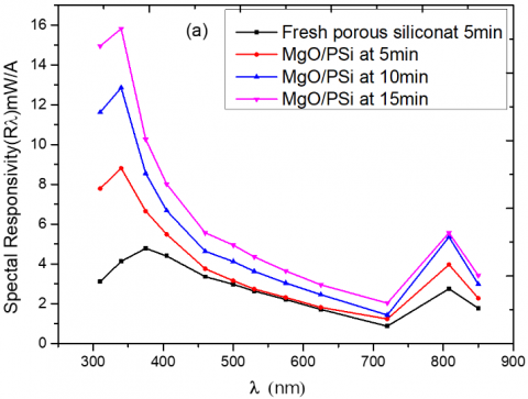
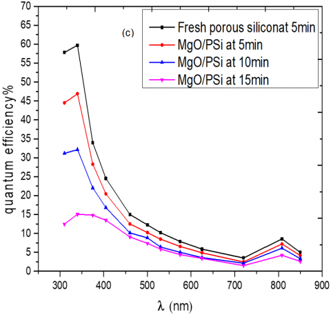
Figure 18 illustrated the responsivity and detectivity of the MgO/PSi as a function of wavelength at etching time (5, 10 and 15min). It can be seen, two peaks of the curves were observed, firstly, the top response position at the spectrum of ultraviolet part of responsivity and detectiviity were displayed specially at(300-400nm) and the second region at low response near IR region (720-850nm). It should be noted,the responsivity and detectivity of all samples increase with increasing etching time, the maximum values of responsivity and detectivity were found to be 15.82 mW/A and 3.75×10¹² Jones at 15min respectively. as Figure 18(a) and (b). The quantum efficiency as a value of wavelength was observed as Figure 18(c). Furthermore, the optimum values of quantum efficiency of MgO/PSi were found to be 59% and 32% at wavelength (300-400nm), and drops values to 8% and 6%, at the near infrared range respectively. Clearly, the performance of the deposited MgO layer improved with increasing etching time due to large surface area [37].
Figure 18. MgO/porous silicon thin films at various etching time (a) Responsivity, (b) Detectiviity, (c) Quantum efficiency
Addionallly, Figure19 exhibits that the MgO thin films have a good photoconductivity and electrical stability under light cycling. The parameters of time rise and time fall were found to be 0.31sec to 0.32 sec respectively.
Figure 19. Time rise and time fall of MgO/porous silicon thin films
MgO thin film nanostructure was prepared using chemical spray method. The structure and morphological properties depended on fabrication conditions. The magnesium oxide has cubic crystal structure. The porous silicon has sponge like structure with network of pores. The optical properties show that the MgO thin film visible in the region has high transmission. It can observed, The energy gap value of the deposited film decreases with increasing number of spraying and was found to be 4.0, 3.95, 3.85eV at 10, 20 and 30. I–V measurements of deposited films display rectifying behavior of all samples. The responsivity, detectivity and quantum efficiency values increase with increasing etching time. The optimization of photodetector can be supported in optical and electrical applications.
4.1 Future suggestion
Studying the effect of the current density and HF concentration on the performance of porous silicon substrate in order to improve the efficiency of the device. Additionally, the effect of annealing tempreatures on the performance porous silicon at various concentrations.
The authors represent thanks to the university of Mosul/Iraq for their facilities and logistic support.
[1] Płóciennik, P., Guichaoua, D., Zawadzka, A., Korcala, A., Strzelecki, J., Trzaska, P., Sahraoui, B. (2016). Optical properties of MgO thin films grown by laser ablation technique. Optical and Quantum Electronics, 48: 1-12. https://doi.org/10.1007/s11082-016-0536-8
[2] Sagadevan, S., Venilla, S., Marlinda, A.R., Johan, M., et al. (2020). Effect of synthesis temperature on the morphologies, optical and electrical properties of MgO nanostructures. Journal of Nanoscience and Nanotechnology, 20(4): 2488-2494. https://doi.org/10.1166/jnn.2020.17185
[3] Alhamd, O.A., Ali, G.G., Aljuboori, M.S.H. (2024). Study and characterization of copper and titanium oxides nanostructures for some molecular and biological applications. Trends in Sciences, 21(4): 7402. https://doi.org/10.48048/tis.2024.7402
[4] Ali, G.G., Ahmed, M.A., Sulaiman, A.A. (2022). Structural properties of AuNPs/PSi nanostructure. Digest Journal of Nanomaterials and Biostructures, 17(2): 473-480. https://doi.org/10.15251/DJNB.2022.172.473
[5] Karthik, K., Dhanuskodi, S., Gobinath, C., Prabukumar, S., Sivaramakrishnan, S. (2019). Ultrasonic-assisted CdO–MgO nanocomposite for multifunctional applications. Materials technology, 34(7): 403-414. https://doi.org/10.1080/10667857.2019.1574963
[6] Visweswaran, S., Venkatachalapathy, R., Haris, M., Murugesan, R. (2020). Characterization of MgO thin film prepared by spray pyrolysis technique using perfume atomizer. Journal of Materials Science: Materials in Electronics, 31(17): 14838-14850. https://doi.org/10.1007/s10854-020-04046-7
[7] Ali, G.G., Hussein, H.A., Khudhur, A.H. (2024). Analytical modelling study of CZTS thin film solar cell for high efficiency performance. Revue des Composites et des Matériaux Avancés-Journal of Composite and Advanced Materials, 34(5): 667-672. https://doi.org/10.18280/rcma.340515
[8] Khanfar, H.K., Qasrawi, A.F. (2015). Performance of the Au/MgO/Ni photovoltaic devices. Materials Science in Semiconductor Processing, 29: 183-187. https://doi.org/10.1016/j.mssp.2014.02.015
[9] Eroğlu, A., Demirezen, S., Azizian-Kalandaragh, Y., Altındal, Ş. (2020). A comparative study on the electrical properties and conduction mechanisms of Au/n-Si Schottky diodes with/without an organic interlayer. Journal of Materials Science: Materials in Electronics, 31: 14466-14477. https://doi.org/10.1007/s10854-020-04006-1
[10] Yildirim, G.B., Daş, E. (2023). The synthesis of MgO and MgO-graphene nanocomposite materials and their diode and photodiode applications. Physica Scripta, 98(8): 085911. https://doi.org/10.1088/1402-4896/ace249
[11] Aouati, R., Djaaboube, H., Bouabelloul, A., Taabouche, A., Bouachiba, Y., Daranfad, W., Oudina, A., Kharfi, F. (2021). Structural and optical properties of MgO thin films prepared by dip-coating process: Effect of thickness. Semiconductors, 55(7): 583-590. https://doi.org/10.1134/S1063782621070058
[12] Toprak, B.Ç., Efkere, H.İ., Aydın, S.Ş., Tataroğlu, A., Özçelik, S. (2024). Structural, morphological, optical and electrical characterization of MgO thin films grown by sputtering technique on different substrates. Journal of Materials Science: Materials in Electronics, 35(20): 1389. https://doi.org/10.1007/s10854-024-13116-z
[13] Sulaiman, E.M., Mutlak, F.A., Nayef, U.M. (2022). High-performance photodetector of Au–MgO/PS nanostructure manufactured via pulsed laser ablation technique. Optical and Quantum Electronics, 54(11): 744. https://doi.org/10.1007/s11082-022-04156-y
[14] Maiti, P., Das, P.S., Bhattacharya, M., Mukherjee, S., Saha, B., Mullick, A.K., Mukhopadhyay, A.K. (2017). Transparent Al+3 doped MgO thin films for functional applications. Materials Research Express, 4(8): 086405. https://doi.org/10.1088/2053-1591/aa8279
[15] Bazhan, Z., Ghodsi, F.E., Mazloom, J. (2013). Effect of stabilizer on optical and structural properties of MgO thin films prepared by sol–gel method. Bulletin of Materials Science, 36: 899-905. https://doi.org/10.1007/s12034-013-0554-0
[16] Iacobucci, S., Offi, F., Torelli, P., Petaccia, L. (2019). Effective attenuation lengths of low energy electrons in MgO thin films. Journal of Electron Spectroscopy and Related Phenomena, 233: 1-4. https://doi.org/10.1016/j.elspec.2019.03.002
[17] Kariper, İ.A., Tezel, F.M. (2019). UV region supercapacitor: Bi-doped natural MgO rock salt thin film. Ceramics International, 45(7): 9219-9224. https://doi.org/10.1016/j.ceramint.2019.01.267
[18] Tigunta, S., Khlikhum, P., Kidkhunthod, P., Chanlek, N., Supadee, L., Pojprapai, S. (2019). Dissolution behavior of MgO thin film-barrier magnetic tunneling junctions. Journal of Materials Science: Materials in Electronics, 30: 6718-6724. https://doi.org/10.1007/s10854-019-00983-0
[19] Güney, H., İskenderoğlu, D. (2018). Synthesis of MgO thin films grown by SILAR technique. Ceramics International, 44(7): 7788-7793. https://doi.org/10.1016/j.ceramint.2018.01.210
[20] Tlili, M., Nefzi, C., Alhalaili, B., Bouzidi, C., Ajili, L., Jebbari, N., Vidu, R., Turki Kamoun, N. (2021). Synthesis and characterization of MgO thin films obtained by spray technique for optoelectronic applications. Nanomaterials, 11(11): 3076. https://doi.org/10.3390/nano11113076
[21] Mhetre, M.T., Pathan, H.M., Thakur, A.V., Lokh, B.J. (2022). Preparation of magnesium oxide (MgO) thin films by spray pyrolysis and its capacitive characterizations. ES Energy & Environment, 18(2): 41-46. https://doi.org/10.30919/esee8c785
[22] El-Gamal, S., El Sayed, A.M. (2019). Physical properties of the organic polymeric blend (PVA/PAM) modified with MgO nanofillers. Journal of Composite Materials, 53(20), 2831-2847. https://doi.org/10.1177/0021998319840802
[23] Mousa, A.O., Nema, N.A., Trier, S.H. (2016). Study of structural and optical properties for MgO films prepared by using chemical spray pyrolysis technique. Materials Science: An Indian Journal, 14(11): 426-434. https://doi.org/10.26565/2312-4334-2023-2-17
[24] Kaneko, S., Ito, T., Soga, M., Motoizumi, Y., Yasui, M., Hirabayashi, Y., Ozawa, T., Yoshimoto, M. (2013). Growth of nanocubic MgO on silicon substrate by pulsed laser deposition. Japanese Journal of Applied Physics, 52(1S): 01AN02. https://doi.org/10.7567/JJAP.52.01AN02
[25] Ali, G.G., Karomi, I.B., Sulaiman, A.A., Mohammed, A.M. (2020). Properties of P-type porous silicon bombarded by neutrons. Nuclear Instruments and Methods in Physics Research Section B: Beam Interactions with Materials and Atoms, 468: 23-27. https://doi.org/10.1016/j.nimb.2020.02.022
[26] Al-Douri, Y., Badi, N., Voon, C.H. (2017). Etching time effect on optical properties of porous silicon for solar cells fabrication. Optik, 147: 343-349. https://doi.org/10.1016/j.ijleo.2017.08.107
[27] Omar, K., Salman, K.A. (2017). Effects of electrochemical etching time on the performance of porous silicon solar cells on crystalline n-type (100) and (111). Journal of Nano Research, 46: 45-56. https://doi.org/10.4028/www.scientific.net/JNanoR.46.45
[28] Xu, J., Liu, S., Yang, Y., Li, J., Tian, C., Guo, L., Zhang, S., Liu, Y., Zhong, Z. (2019). Preparation of porous silicon by electrochemical etching methods and its morphological and optical properties. International Journal of Electrochemical Science, 14(6): 5188-5199. https://doi.org/10.20964/2019.06.10
[29] Jansen, D., Naber, C., Ectors, D., Lu, Z., Kong, X.M., Goetz-Neunhoeffer, F., Neubauer, J. (2018). The early hydration of OPC investigated by in-situ XRD, heat flow calorimetry, pore water analysis and 1H NMR: Learning about adsorbed ions from a complete mass balance approach. Cement and Concrete Research, 109: 230-242. https://doi.org/10.1016/j.cemconres.2018.04.017
[30] Zulkefle, H., Ismail, L.N., Bakar, R.A., Mahmood, M.R. (2011). Molar concentration effect on MgO thin films properties. In 2011 IEEE Symposium on Industrial Electronics and Applications, Langkawi, Malaysia, pp. 468-471. https://doi.org/10.1109/ISIEA.2011.6108754
[31] Aziz, S.I., Ali, G.G. (2025). Enhancement of performance CdxPb1-xS/porous silicon heterojunction photodetector by chemical spray pyrolysis method. Chalcogenide Letters, 22(3): 239-253. https://doi.org/10.15251/CL.2025.223.239
[32] Aksay, S. (2019). Effects of Al dopant on XRD, FT-IR and UV–vis properties of MgO films. Physica B: Condensed Matter, 570: 280-284. https://doi.org/10.1016/j.physb.2019.06.020
[33] Raj, A.M.E., Jayachandran, M., Sanjeeviraja, C. (2010). Fabrication techniques and material properties of dielectric MgO thin films—A status review. CIRP Journal of Manufacturing Science and Technology, 2(2): 92-113. https://doi.org/10.1016/j.cirpj.2010.02.003
[34] Younus, M. H., Ali, G.G., Salih, H.A. (2021). The reinforced optical fiber sensing with bilayer AuNPs/SiC for pressure measurement: Characterization and Optimization. Journal of Physics: Conference Series, 1795(1): 012002. https://doi.org/10.1088/1742-6596/1795/1/012002
[35] Ahmed, A.A., Dahham, N.A., Ali, G.G. (2024). Optical properties of CuS/porous silicon heterojunction. Iraqi Journal of Applied Physics, 20(3A): 505-510.
[36] Mohammed, M.S., Shlaga, R.A. (2019). Morphological and optical properties of porous silicon. Engineering and Technology Journal, 37(1B): 17-20. https://doi.org/10.30684/etj.37.1B.3
[37] Ahmed, A.A., Ali, G.G., Daham, N.A. (2024). Performance of high sensitive heterojunction CuS/porous silicon photodetector. Chalcogenide Letters, 21(1): 81-97. https://doi.org/10.15251/CL.2024.211.81