Abdelhaq Dahmani*![]() | Kamal Himour
| Kamal Himour![]() | Yacine Guettaf
| Yacine Guettaf![]()
© 2023 IIETA. This article is published by IIETA and is licensed under the CC BY 4.0 license (http://creativecommons.org/licenses/by/4.0/).
OPEN ACCESS
In this study we propose the optimization of the power quality in photovoltaic systems connected to grid. This system is composed of a grid powered by a photovoltaic generator (PVG) through two static converters controlled independently. A boost converter is a power electronic circuit that steps up a DC voltage to a higher level while regulating the output voltage of the PVG. this converter is control by incremental conductance (IC) which is one of the best maximum power point tracker technics (MPPT) to extract maximum power of the PVG, by dynamically modifying the operating voltage based on the instantaneous slope of the power-voltage curve. For a best quality of voltage and current injected to grid we use the simplified pulse width modulation (PWM) to command different structures of three-level inverters: A three-phase three-level flying capacitor (FC), a three-phase three-level neutral point clamped (NPC) and an active neutral point clamped (ANPC) three-phase three-level inverter. The proposed system was simulated in MATLAB Simulink to demonstrate its effectiveness in improving the power quality when injecting power from a photovoltaic generator (PVG) into the grid.
PVG, incremental conductance, three-level flying capacitor inverter, boost converter, pulse width modulation, THD
Photovoltaic systems make it possible to exploit the energy of the sun for various purposes. They are very reliable and provide a non-polluting source of electricity that can be used for a range of applications. Among the interesting applications of this form of energy is its integration into the power grid.
Several research works have been carried out in this axis by proposing multilevel structures for the connection of PV generators to the power grid, such as neutral point clamped inverter [1], H bridge inverter [2], FC inverter [3], ANPC [4] and There are many other hybrids inverters [5, 6].
Multilevel inverter structures are chosen for their distinct advantages over conventional configurations. These structures offer enhanced efficiency, reduced harmonic distortion, and improved overall performance in grid-connected photovoltaic systems.
In this study, we will present different structures of multilevel inverter used as an interface for the connection of a PVG to the power grid, flying capacitor multilevel inverter, neutral point clamped and active neutral point clamped. These structures offer advantages over the conventional structure.
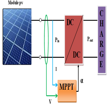
First, we developed the mathematical model of PVG connected to grid, the global system is composed of the following elements: a PV generator, a DC-DC converter, an inverter, a filter and the grid.
The control mechanism of this system is divided into three parts:
1. MPPT control to maximize the power output from the PVG by acting on boost converter.
2. The voltage control which focuses on maintaining a stable voltage level in the DC bus system of the photovoltaic system. by regulating the voltage, it ensures the generation of a consistent reference current, a crucial parameter for controlling the multilevel inverter.
3. PWM technique to control the multilevel inverter by adjusting the pulse widths, the amplitude and frequency of the output voltage can be precisely manipulated.
The photovoltaic-grid system is comprised of the following components: a photovoltaic generator, a boost converter, a maximum power point tracking controller, a three-level inverter, an RL filter, and the grid. This system is shown in Figure 1.
Figure 1. Global system of PVG connected to grid
2.1 Modelling of the photovoltaic generator
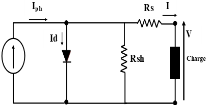
The real equivalent circuit design of a photovoltaic cell is illustrated in Figure 2.
Figure 2. Equivalent circuit of photovoltaic cell
The current-voltage (I-V) characteristic for a PVG cell can be described as follows:
$I=I_{p h}-I_s\left[\left(\exp \frac{V+I \cdot R_s}{m \cdot \frac{K \cdot T}{q}}\right)-1\right]-\frac{V+I \cdot R_s}{R_{s h}}$ (1)
The current-voltage characteristic for a PV panel that has $N_s$ cells connected in series and $N_P$ cells connected in parallel is given by the following expression:
$\begin{gathered}I=N_p \cdot I_{p h}-N_p \cdot I_s\left[\exp \left\langle\left(\frac{1}{m \cdot K \cdot T / q}\right) \cdot\left(\frac{V}{N_s}+\frac{R_s \cdot I}{N_p}\right)\right\rangle-\right. 1]-\frac{N_p}{R_{s h}} \cdot\left(\frac{V}{N_s}+\frac{R_s \cdot I}{N_p}\right)\end{gathered}$ (2)
Photovoltaic panel model. In our study, we chose the Sun Power SPR-305E-WHT-D model for many factors such as accuracy and realism, as the model's characteristics closely resemble real-world solar panels, ensuring accuracy in representative simulations. In addition, our selection is driven by the alignment of specific model characteristics with research objectives, especially when investigating efficiency, energy productivity, or responses to different environmental conditions. Simulink's provision of pre-built libraries for this model further supports this choice, facilitating seamless integration and compatibility into the simulation environment with other system components, simplifying the simulation process. Furthermore, prior use of the Sun Power SPR-305E-WHT-D and its validation in other studies has strengthened our confidence in its consistency and comparability, confirming its suitability for achieving reliable results.
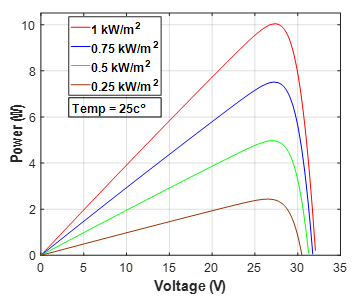
Figure 3. Irradiation effect on the power-voltage characteristic
Figure 4. Temperature effect on the power-voltage characteristic
For SunPowerSPR-305E-WHT-D (Neser=5, Nar=66) PV panel, Figure 3 shows the effect of irradiation for the power-voltage characteristic of this PV panel.
Figure 4 illustrates the temperature effect for the power-voltage characteristic of this PV panel.
2.2 Model of boost converter
A DC-DC converter acts as a switch-mode regulator to transform an unregulated DC voltage to a regulated DC output voltage. The regulation is usually achieved through PWM and the switching device commonly used is either a MOSFET or an IGBT. The primary function of a boost DC-DC converter is to increase the DC voltage. The configuration of a DC-DC boost converter with a PV system as the input is depicted in Figure 5. Maximum power is reached when the MPPT algorithm changes and adjusts the duty cycle of the boost DC-DC converter [7].
Figure 5. Boost converter
The mathematical expressions that control the operation of the converter are presented as follows:
$V_o=\frac{V}{(1-\alpha)}$ (3)
$I_o=I \cdot(1-\alpha)$ (4)
2.3 Three-level inverter models
2.3.1 Model and control of FC inverter
The flying capacitor three-level three-phase inverter is depicted in Figure 6. This term is applied due to the floating nature of the capacitor with respect to the earth's potential. Thus, a three-level flying capacitor inverter consists of four switches, two main capacitors & one auxiliary capacitor in each leg [8].
Figure 6. Flying capacitor three level inverter (FC) [9]
The output voltage is shown in Table 1.
Table 1. States of one leg of FC inverter
|
$\mathbf{F}_{\mathbf{k} \mathbf{1}}$ |
$\mathbf{F}_{\mathbf{k} \mathbf{2}}$ |
$\mathbf{F}_{\mathbf{k} \mathbf{3}}$ |
$\mathbf{F}_{\mathbf{k} \mathbf{4}}$ |
$\mathbf{V}_{\mathbf{k}}$ |
State |
|
1 |
1 |
0 |
0 |
Uc/2 |
P |
|
1 |
0 |
1 |
0 |
0 |
O |
|
0 |
1 |
0 |
1 |
0 |
|
|
0 |
0 |
1 |
1 |
-Uc/2 |
N |
As outlined in Table 1, each leg of the inverter can assume one of three potential switching states: positive (P), Zero (O), or negative(N). Activation of the top two switches (Ti1 and Ti2) results in switching state P and the corresponding output voltage is positive(+Uc/2). When the medium switches Ti2 and Ti3 are turned on switching state is O, and the output voltage is zero. Lastly, when the lower switches (Ti3 and Ti4) are turned on, the switching state becomes N, and the corresponding output voltage is negative(-Uc/2)
For any initial state of FC inverter, the inverter output voltages are giving by:
$V_{A N}=S_1\left(V_{C 1}-V_{C 2}\right)+S_2 V_{C 2}-\frac{V_{C 1}}{2}$ (5)
2.3.2 Model and control of NPC inverter
Figure 7. Neutral point clamped three level inverter (NPC)
The diagram in Figure 7 displays the detailed configuration of the NPC inverter. The inverter consists of a DC bus and three legs, each of which contains four IGBTs, four free-wheeling diodes, and two clamping diodes. The antiparallel connection of each free-wheeling diode with the power switch forms a reverse conduction path for the current. The DC bus includes two capacitors (C1 and C2), providing the midpoint "O". Capacitors can absorb the power difference between the rectifier and the inverter, and support the dc link. denotes the dc-link voltage [10].
Connection functions. Three connection functions are defined for each leg of the inverter, and each function corresponds to one of the three states of the leg:
$\left\{\begin{array}{l}F_{c 1 j}=F_{1 j} \cdot F_{2 j} \\ F_{c 2 j}=F_{2 j} \cdot F_{3 j} \\ F_{c 3 j}=F_{3 j} \cdot F_{4 j}\end{array}\right.$ (6)
Table 2. States of one leg of NPC inverter
|
$\mathbf{F}_{\mathbf{k} \mathbf{1}}$ |
$\mathbf{F}_{\mathbf{k} \mathbf{2}}$ |
$\mathbf{F}_{\mathbf{k} \mathbf{3}}$ |
$\mathbf{F}_{\mathbf{k} \mathbf{4}}$ |
$\mathbf{V}_{\mathbf{k}}$ |
State |
|
0 |
0 |
1 |
1 |
-Uc/2 |
N |
|
0 |
1 |
1 |
0 |
0 |
O |
|
1 |
1 |
0 |
0 |
Uc/2 |
P |
Table 2 demonstrates that each segment of the NPC inverter has the capability to have one of three distinct switching states: P, O, N.
Output voltages. The output voltages of NPC inverter are expressed as follows:
$\left[\begin{array}{l}V_{10} \\ V_{20} \\ V_{30}\end{array}\right]=\left[\begin{array}{lll}F_{c 11} & F_{c 21} & F_{c 31} \\ F_{c 12} & F_{c 22} & F_{c 32} \\ F_{c 13} & F_{c 23} & F_{c 33}\end{array}\right] \cdot\left[\begin{array}{c}\frac{U c}{2} \\ 0 \\ -U c \\ 2\end{array}\right]$ (7)
We define the output voltage vector as follows, based on the voltages $V_{10}$, $V_{20}$ et $V_{30}$:
$V_s=V_{10} e^{j 0}+V_{20} e^{-j 2 \pi / 3}+V_{30} e^{j 2 \pi / 3}$ (8)
$V_s=V_d+j V_q$ (9)
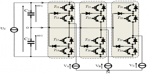
2.3.3 Model and control of ANPC inverter
The fundamental structure of the three-phase, three-level active neutral point clamped (ANPC) inverter is depicted in Figure 8. It is evident that each phase incorporates two supplementary active switches that are connected in reverse parallel with the clamping diodes. Since the modulation strategy is the same for each phase, analysis on one phase leg is sufficient [11].
Figure 8. Active neutral point clamped three level inverter (ANPC)
For one phase, the relation of switching states and the output voltage is shown in Table 3.
Table 3. States of one leg of ANPC inverter
|
$\mathbf{F}_{\mathbf{k} \mathbf{1}}$ |
$\mathbf{F}_{\mathbf{k} \mathbf{2}}$ |
$\mathbf{F}_{\mathbf{k} \mathbf{3}}$ |
$\mathbf{F}_{\mathbf{k} \mathbf{4}}$ |
$\mathbf{F}_{\mathbf{k} \mathbf{5}}$ |
$\mathbf{F}_{\mathbf{k} \mathbf{6}}$ |
$\mathbf{V}_{\mathbf{k}}$ |
State |
|
1 |
1 |
0 |
0 |
0 |
0 |
Uc/2 |
P |
|
0 |
1 |
0 |
0 |
1 |
0 |
0+ |
O |
|
0 |
0 |
1 |
0 |
0 |
1 |
0- |
|
|
0 |
0 |
1 |
1 |
0 |
0 |
-Uc/2 |
N |
Table 3 demonstrates that each segment of the ANPC inverter also has the capability to have one of three distinct switching states: P, O, N.
2.4 Filter model
A basic type of filter is the line inductance, commonly referred to as an L-filter (as shown in Figure 9). The ideal characteristic of this filter is that its impedance increases as the frequency increases, thereby increasing the reduction of high-frequency signals. The transfer function matrix of an L-filter in the Laplace domain is simply written as [12]:
$Y_L^s=\left[\begin{array}{cc}\frac{1}{s L_t+R_t} & 0 \\ 0 & \frac{1}{s L_t+R_t}\end{array}\right]$ (10)
Figure 9. Filter RL
2.5 Main control strategies
The objective of the global system controller is to maximize the power delivered by the PV generator, regulate the DC-link voltage, set a unit power factor and to control the switches of the multilevel inverter.
2.5.1 MPPT control (IC)
Figure 10. MPPT control (IC)
The MPPT algorithm employs the principle of generating disturbances by varying the cyclic ratio α and monitoring its impact on the power output of the PVG. It utilizes the instantaneous conductance I/V and the incremental conductance dv/di for MPPT. This approach is illustrated in Figure 10.
Figure 11 presents its algorithm.
Figure 11. IC algorithm [13]
2.5.2 DC bus control
The DC voltage controller is responsible for regulating the DC bus and setting the reference active power, $P_{g~ref }$. The block diagram of the DC voltage control system is displayed in Figure 12.
Figure 12. DC bus control block diagram
2.5.3 Power control
The expression for active and reactive power $\left(P_g, Q_g\right)$ can be represented using the Park components of the supply voltage $\left(V_{t d}, V_{t q}\right)$ and line current $\left(I_{t d}, I_{t q}\right)$ as indicated below:
$\left\{\begin{array}{l}P_g=V_{t d} \cdot I_{t d}+V_{t q} \cdot I_{t q} \\ Q_g=V_{t d} \cdot I_{t q}-V_{t q} \cdot I_{t d}\end{array}\right.$ (11)
Reference currents $\left(I_{td ref }, I_{tq ref }\right)$ are used to establish the desired reference active and reactive powers $\left(P_{g ref}, Q_{g ref}\right)$, as follows:
$\left\{\begin{array}{l}I_{t d ~ r e f}=\frac{P_{g ~ r e f} \cdot V_{t d}-Q_{g ~r e f} \cdot V_{t q}}{V_{t d}{ }^2+V_{t q}{ }^2} \\ I_{t q ~ r e f}=\frac{P_{g ~ r e f} \cdot V_{t q}+Q_{g ~ r e f} \cdot V_{t d}}{V_{t d}{ }^2+V_{t q}{ }^2}\end{array}\right.$ (12)
A unity power factor refers to a condition in an electrical system where the phase angle between the voltage and current waveforms is zero, resulting in an ideal power factor of 1.
This power factor can be achieved by setting the reactive power reference to zero. Additionally, the system can generate or absorb reactive power by adjusting the reactive power reference to be either negative or positive:
$\left\{\begin{array}{l}Q_{\text {g ref }}<0 \\ Q_{\text {g ref }}>0\end{array}\right.$ (13)
2.5.4 Current control
The execution of vector current control in the park reference frame involves synchronizing the reference with the grid voltage. The electrical equations for the filter ($R_t, L_t$) are detailed as follows:
$\left\{\begin{array}{l}V_{t d}=R_t I_{t d}+L_t \frac{d I_{t d}}{d t}-\omega_s L_t I_{t d}+V_{s d} \\ V_{t q}=R_t I_{t q}+L_t \frac{d I_{t q}}{d t}+\omega_s L_t I_{t q}+V_{s q}\end{array}\right.$ (14)
Current control block diagram is illustrated in Figure 13.
Figure 13. Current control block diagram
2.5.5 PWM control
Pulse Width Modulation (PWM) is a technique for controlling the switches of a three-phase three-level inverter. The intersective PWM method is a simple way to generate the PWM pulse train in response to a given signal. As illustrated in Figure 14, a sine wave (blue) is compared with a triangle wave (red) and when the triangle wave is less than the sine wave, the PWM output signal (green) is set to a high level (1). Conversely, it is set to a low level (0).
The level switching edge is produced at every moment the sine wave intersects the triangle wave. Thus, the different crossing positions result in variable duty cycle of the output waveform [14].
where:
$\left\{\begin{array}{l}m a=\frac{V_{m .s i n}}{V_{m . t r i}}=0.8 \\ m f=\frac{f_{t r i}}{f_{\text {sin }}}=200\end{array}\right.$ (15)
Figure 14. PWM principle
Combined, the control strategies establish a complementary relationship, promoting a coordinated and synchronized approach to power generation, conversion, and delivery. MPPT technique plays a pivotal role in optimizing power generation. DC bus control generates a stable voltage, this stable voltage supports efficient PWM modulation. In turn, PWM guarantees that the multi-level inverter output aligns with grid integration standards, which contribute to stable and reliable power supply in the PV system, ensuring its efficient performance in real-world applications.
Within this portion, we present the results of our simulation of the PV-GRID system using MATLAB Simulink, this simulation was carried out to evaluate different models of three-level inverters. Firstly, we extracted from the simulation irradiance, temperature and corresponding power provided by the PVG, and we also extracted the power provided by the boost converter. Then we extracted the current and voltage of grid and their THD for each model of three-level inverter.
Finally, we discuss and comment on these results and compare them.
At first, we proposed that the up/down of irradiance and temperature as it is illustrated in Figure 15.
Figure 15. Up/down of irradiance and temperature
For that up/down of irradiance and temperature the mean power of PV generator is shown in Figure 16.
Figure 16. Mean power of PV generator
Then the voltage of DC bus is shown in Figure 17 below.
Figure 17. DC bus voltage
After that we extract the voltage, current and THD figures for each model of multilevel inverter, see Figures 18-29 below.
1. FC Inverter
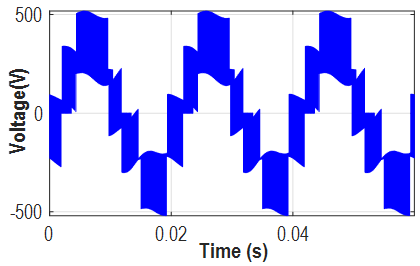
Figure 18. FC output voltage
Figure 19. THD of output voltage
Figure 20. Current injected to grid
Figure 21. Current THD injected to grid
2. NPC Inverter
Figure 22. NPC output voltage
Figure 23. THD of output voltage
Figure 24. Current injected to grid
Figure 25. Current THD injected to grid
3. ANPC Inverter
Figure 26. ANPC output voltage
Figure 27. THD of output voltage
Figure 28. Current injected to grid
Figure 29. Current THD injected to grid
4. Comments
Through the simulation results, we notice that the RL filter effectively reduces harmonic content in both absorbed current and voltage signals, and this is crucial for improving the power quality injected to grid.
The study compares three inverter topologies: FC, NPC and ANPC, the almost identical output voltage values indicate that all three inverters are capable of generating comparable fundamental components.
The THD values provide insights into the purity of the generated waveform. Lower THD values, as seen in the case of ANPC (43.28% for voltage and 0.96% for current), indicate a closer approximation to an ideal sinusoidal waveform.
The best performance of the ANPC inverter in terms of THD is significant. It implies that this inverter introduces less distortion to the grid, ensuring a higher-quality power supply with fewer harmonic components.
The peak voltage values for each inverter topology represent the maximum amplitude of the fundamental component. These values, despite being close, might have implications for equipment compatibility and safety margins.
The low peak current values for all inverters suggest efficient power transfer with minimized stress on the components.
Also, from the perspective of components used, the FC inverter is more interesting, considering cost, reliability, and ease of implementation.
We have summarized our study “Optimization of power quality in photovoltaic systems connected to grid” in Table 4.
Table 4. Comparison table of different topologies
|
Topologies |
FC |
NPC |
ANPC |
|
Peak voltage value of the fundamental component (V) |
330.90 |
321.60 |
321.90 |
|
Voltage TDH (%) |
54.38 |
43.47 |
43.28 |
|
Peak current value of the fundamental component (A) |
3.138 |
3.122 |
3.133 |
|
Current TDH (%) |
16.25 |
1.02 |
0.96 |
The study's result highlights the outstanding performance of the ANPC inverter, supported by remarkably low THD values for both current (0.96%) and voltage (43.28%). It is classified as an ideal option for enhancing power quality in grid-connected photovoltaic systems.
The broader implications of the study underscore the critical role of inverter topology in enhancing power quality, indicating the potential for significant improvements in overall performance and reliability and opening up prospects for practical applications, ensuring a cleaner, more stable power supply. Investment in advanced inverter technologies, specifically ANPC, is proposed as a strategic approach to meeting power quality standards and contributing to the sustainability and efficiency of the broader energy infrastructure.
As for future work, the study suggests exploring various inverter models and configurations and investigating emerging technologies and hybrid setups to enhance power quality metrics. It also recommends improving simulation models and considering a wider range of environmental conditions to gain a more comprehensive understanding of inverter performance.
This work is part of the preparation for a doctorate in electrical engineering, with the support and supervision of the Algerian Ministry of Higher Education and Scientific Research (2023).
|
PVG |
photovoltaic generator |
|
MPPT |
maximum power point tracker |
|
IC |
incremental conductance |
|
PWM |
pulse width modulation |
|
THD |
total harmonic distortion |
|
Cb |
boost conductance, mF |
|
f |
Frequency, Hz |
|
fs |
switching frequency, KHz |
|
Iph |
the photo-current, A |
|
IS |
the saturation current of diode, A |
|
ISC |
current of short circuit, A |
|
Io |
output current of the Boost converter, A |
|
Iop |
optimal current, A |
|
K |
Boltzmann constant, J. K-1 |
|
L |
filter inductance, mH |
|
Lb |
boost inductance, mH |
|
m |
ideality factor |
|
ma |
amplitude modulation index |
|
mf |
frequency modulation index |
|
Np |
series panels number |
|
Ns |
parallel panels number |
|
P |
grid power, KW |
|
Pmax |
maximum PVG power, W |
|
q |
electron charge, c |
|
R |
filter resistance, m$\Omega$ |
|
Rb |
boost resistance, m$\Omega$ |
|
Rs, Rsh |
series and parallel resistance $\Omega$ |
|
T |
junction temperature, ℃ |
|
TISC |
short circuit current temperature coefficient, A |
|
TS |
sampling period, ms |
|
TVOC |
open circuit voltage temperature coefficient, V |
|
Vg |
grid voltage, KV |
|
VO |
output voltage of the boost converter, V |
|
VOC |
voltage of open circuit, V |
|
VOP |
optimal voltage, V |
|
$\alpha$ |
the cyclic ratio $\alpha$ |
Table A1. System parameters
|
Photovoltaic Array |
|
|
Model |
Sun power SPR-305E-WHT-D |
|
Ns |
5 |
|
Np |
66 |
|
Pmax |
305 |
|
VOP |
54.7 |
|
IOP |
5.58 |
|
VOC |
64.2 |
|
ISC |
5.96 |
|
TVOC |
-0.27269 |
|
TISC |
0.061745 |
|
Boost Converter |
|
|
Vin |
250 |
|
fs |
5 |
|
Ts |
0.2 |
|
$\alpha$ |
0.5 |
|
Cb |
0.1 |
|
Rb |
5 |
|
Lb |
5 |
|
DC Bus |
|
|
Udc |
500 |
|
PWM |
|
|
ma |
0.8 |
|
mf |
200 |
|
Filter |
|
|
R |
19 |
|
L |
0.25 |
|
Grid |
|
|
P |
100 |
|
Vg |
120 |
|
f |
50 |
[1] Sebaaly, F., Vahedi, H., Kanaan, H.Y., Moubayed, N., Al-Haddad, K. (2016). Finite control set model predictive controller for grid connected inverter design. In 2016 IEEE International Conference on Industrial Technology (ICIT), Taipei, Taiwan, pp. 1208-1213. https://doi.org/10.1109/ICIT.2016.7474926
[2] Guerriero, P., Coppola, M., Di Napoli, F., Brando, G., Dannier, A., Iannuzzi, D., Daliento, S. (2016). Three-phase PV CHB inverter for a distributed power generation system. Applied Sciences, 6(10): 287. https://doi.org/10.3390/app6100287
[3] Hammami, M., Ricco, M., Ruderman, A., Grandi, G. (2019). Three-phase three-level flying capacitor PV generation system with an embedded ripple correlation control MPPT algorithm. Electronics, 8(2): 118. https://doi.org/10.3390/electronics8020118
[4] Li, J., Huang, A.Q., Liang, Z., Bhattacharya, S. (2011). Analysis and design of active NPC (ANPC) inverters for fault-tolerant operation of high-power electrical drives. IEEE Transactions on Power Electronics, 27(2): 519-533. https://doi.org/10.1109/TPEL.2011.2143430
[5] Manohar, V.J., Rao, K.K. (2017). A hybrid multilevel inverter topology for PV system with high step up DC-DC converter. Journal of Electrical Engineering, 17(3): 8-8.
[6] Prabaharan, N., Palanisamy, K. (2016). A single phase grid connected hybrid multilevel inverter for interfacing photo-voltaic system. Energy Procedia, 103: 250-255. https://doi.org/10.1016/j.egypro.2016.11.28
[7] Zainuri, M.M., Radzi, M.M., Soh, A.C., Rahim, N.A. (2012). Adaptive P&O-fuzzy control MPPT for PV boost DC-DC converter. In 2012 IEEE International Conference on Power and Energy (PECon), Kota Kinabalu, Malaysia, pp. 524-529. https://doi.org/10.1109/PECon.2012.6450270
[8] Esa, M., Nawaz, M.A.M., Naheed, S. (2017). Harmonic Analysis of three level flying capacitor inverter. International Research Journal of Engineering and Technology, 4(10): 1687-1694.
[9] Joca, D.R., Barreto, L.H., Oliveira, D.D.S., Silva, R.N., Henn, G.A. (2012). Modulation technique based on CSV-PWM and HEPWM for THD reduction in flying capacitor multilevel inverters. In 2012 10th IEEE/IAS International Conference on Industry Applications, Fortaleza, Brazil, pp. 1-6. https://doi.org/10.1109/INDUSCON.2012.6453491
[10] Liu, S., Qian, X., Wan, H., Ye, Z., Wu, S., Ren, X. (2020). NPC three-level inverter open-circuit fault diagnosis based on adaptive electrical period partition and random forest. Journal of Sensors, 2020: 1-18. https://doi.org/10.1155/2020/9206579
[11] Zhang, Z. (2017). Investigation of an ANPC Inverter in Electrified Vehicles. Chalmers University of Technology, Gothenburg, Sweden.
[12] Juntunen, R. (2018). LCL Filter Designs for Parallel-Connected Grid Inverters. Lappeenranta University of Technology Scientific Reports (Acta Universitatis Lappeenrantaensis), Finland.
[13] Kareem, P.R. (2019). Simulation of the Incremental conductance algorithm for maximum power point tracking of photovoltaic system based on Matlab. Diyala Journal of Engineering Sciences, 12(1): 34-43. https://doi.org/10.26367/DJES/VOL.12/NO.1/5
[14] Infineon Technologies AG. (2006). Different PWM Waveforms Generation for 3-Phase AC Induction Motor with XC164CS. 81726 München, Germany.