Adel Dahdouh* | Lakhdar Mazouz | Brahim Elkhalil Youcefa
© 2022 IIETA. This article is published by IIETA and is licensed under the CC BY 4.0 license (http://creativecommons.org/licenses/by/4.0/).
OPEN ACCESS
In this paper, an implementation of a feedback linearisation-based on SVM control of a multifunctional unified power quality conditioner (UPQC) combined with a photovoltaic generator (PVG) using STM32F429I-DISC DSP board has been presented. Further, The PVG-UPQC is acting as a universal conditioner for power quality enhancement and renewable energy integration simultaneously with harmonics reduction in both grid voltage and current. Furthermore, the system can also compensate reactive power in presence of nonlinear loads. The presented system is made up of a shunt active power filter which acts as a current harmonics compensator in addition to a series filter that compensates voltage harmonics and fluctuations such as voltage sag/swell. In order to enhancing the PVG-UPQC performances, a nonlinear feedback linearisation control technique combined with SVM controller is applied. The performance of the suggested control scheme is validated by extensive PIL co-simulation technique. The obtained results prove the high performances and reliability of the presented system in the case of nonlinear load variations as well as eliminating voltage and current harmonics. These results accomplish the superiority and effectiveness of those obtained by a compared to a conventional PI controller.
harmonic extraction, photovoltaic generator (PVG), unified power quality conditioner (UPQC), feedback linearisation controller (FLC), space vector modulation (SVM), power quality enhancement
In recent years, due to the increased usage of power electronic equipment, the power quality has been deteriorated owing to harmonic generations [1]. At IEEE-519 and IEC-555, the standards and terminology have been thoroughly specified for power quality. The overall harmonic distortion permitted should be less than 5% according to these rules [2].
With the use of passive filters, the aforementioned issues can be partially overcoming [3-6]. However, this type of filter would not resolve random fluctuations in the load current and voltage waveforms. On the contrary, compensating devices, such as Static Var-Compensator (SVC), Parallel Active-Filter (PAF), Series Active-Filter (SAF) and hybrid filters are suggested to ensure power quality [7]. Further, since these devices are only can tackle one or two power quality issues, their capabilities are typically restricted. Otherwise, Recent studies have demonstrated that unified power quality conditioners (UPQCs), which include series and shunt active filters, could demonstrates the majority of power quality issues at the same time [8].
The UPQC can keep the load end-voltage constant and prevent voltage sags/swells from entering the system [9]. In addition, the UPQC could also effectively supply the load's reactive power requirements and suppress produced load harmonic currents, preventing them from propagating back to the utility, causing voltage and current distortion to other customers [10].
In the literature review, diverse control techniques of UPQC have been presented. Yang & Jin [11] represented a cost-effective energy storage device based UPQC to simultaneously suppress the power oscillations during unbalanced voltage conditions. In fact, the presented results in this paper has not proven the THD of the voltage and the results are not clear. A Three-Phase Solar PV and Battery Energy Storage System Integrated UPQC has presented by Mansor [12], the controller used in this paper is a conventional PI regulator, based on the kind of regulator the results demonstrated are not sufficient and the duration of the simulation can’t prove its robustness. Further, an inductive hybrid UPQC for Power quality management in premium-power-supply required applications has been accomplished by Yu et al. [13], the DC bus voltage as well as the active and reactive powers fluctuations has been demonstrated the inferiority of the proposed control of this paper. A Power quality enhancement in solar power with grid connected system using UPQC has been established [14]. Otherwise, the system does not prove the performances of the controller under nonlinear variations in addition to the high value of the THD that reached 4.66%.
In order to overcome the above mentioned literature papers disadvantages, this paper has been proposed a new control technique based on a feedback linearisation-SVM technique for the PVG-UPQC in the purpose of filtering active and reactive powers within nonlinear load variations, and improving power quality besides current and voltage harmonics with fluctuations such as voltage sag/swell compensations. Moreover, to validate and confirm the robustness and high performances of the suggested controller, a comparison study has been done with a conventional PI through varied simulation results for a nonlinear load. In fact, the obtained reduced THD for both voltage and current harmonic compensations in addition of less fluctuations on the DC link has been well demonstrated along with the proposed controller that guarantee a high performances of power quality on the grid based on the Introduced feedback linearisation-SVM controller.
The remaining part of this paper is organized in the following manner: in section II, the design of different parts of the PVG-UPQC is detailed, while simulation results under different scenarios and their analysis are given in section III and the final section represents the conclusion of the present work.
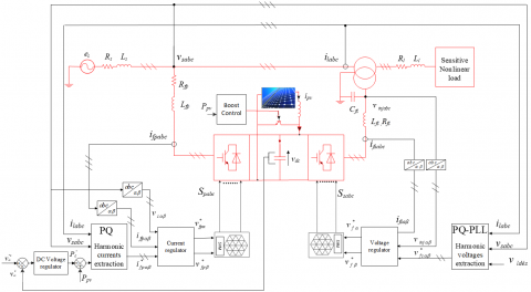
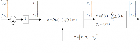
Figure 1 depicts the basic operation of the suggested control approach for the PVG-UPQC associated with a nonlinear load. A two-level Space Vector Modulator generates the switch control signals. The SVM technique has been opted in this paper to achieve several common objectives: reduction of the total harmonic distortion (THD) and therefore less switching losses and giving more possibility of controlling the system with a constant frequency. In addition, the SVM control technique has taken the focusing of many works in controlling their system inverters [15-17].
The instantaneous PQ theory for currents and PQ-PLL for voltages are used to establish the harmonic references [18, 19]. Compensation goals include voltage and current harmonics mitigation, reactive power compensation and DC bus regulation during the bidirectional active power exchange between the PV generator, two active filters and power system grid. A detailed analysis of the different components of PVG-UPQC is presented hereafter.
Figure 1. Feedback linearisation- SVM control scheme of the PVG-UPQC
2.1 Mathematical model of GPV-UPQC
The PVG-UPQC’s dynamic model is described by a differential equation defined in α-β stationary frame. The latter is presented in Eqns. (1) and (3).
The parallel filter model is governed by the following equation [9]:
$\begin{align} & \frac{d{{i}_{fp\alpha }}}{dt}=-\frac{{{R}_{fp}}}{{{L}_{fp}}}{{i}_{fp\alpha }}-\frac{{{v}_{s\alpha }}}{{{L}_{fp}}}+\frac{{{v}_{fp\alpha }}}{{{L}_{fp}}} \\ & \frac{d{{i}_{fp\beta }}}{dt}=-\frac{{{R}_{fp}}}{{{L}_{fp}}}{{i}_{fp\beta }}-\frac{{{v}_{s\beta }}}{{{L}_{fp}}}+\frac{{{v}_{fp\beta }}}{{{L}_{fp}}} \\ \end{align}$ (1)
It can also be written in form (2).
${{\dot{x}}_{p}}={{f}_{p}}({{x}_{p}})+{{g}_{p}}({{x}_{p}}){{u}_{p}}$ (2)
where:
$f_{p}\left(x_{p}\right)=\left[\begin{array}{cc}-\frac{R_{f p}}{L_{f p}} i_{f p \alpha}-\frac{v_{s \alpha}}{L_{f p}} \\ -\frac{R_{f p}}{L_{f p}} i_{f p \beta}-\frac{v_{s \beta}}{L_{f p}}\end{array}\right], g_{p}\left(x_{p}\right)=\left[\begin{array}{cc}\frac{1}{L_{f p}} & 0 \\ 0 & \frac{1}{L_{f p}}\end{array}\right]$, $x_{p}=\left[\begin{array}{c}i_{f p \alpha} \\ i_{f p \beta}\end{array}\right], u_{p}=\left[\begin{array}{c}v_{f p \alpha} \\ v_{f p \beta}\end{array}\right]$
$y_{p}=\left[\begin{array}{l}y_{p 1} \\ y_{p 2}\end{array}\right]=\left[\begin{array}{l}h_{p 1} \\ h_{p 2}\end{array}\right]$ .
vsαβ are source voltages in α-β frame, ifpαβ and vfpαβ are the α-β axis currents and voltages of the shunt filter respectively.
The series filter model is described by [12]:
$\begin{align} & \frac{d{{i}_{fs\alpha }}}{dt}=-\frac{{{R}_{fs}}}{{{L}_{fs}}}{{i}_{fs\alpha }}-\frac{{{v}_{inj\alpha }}}{{{L}_{fs}}}+\frac{{{v}_{fs\alpha }}}{{{L}_{fs}}} \\ & \frac{d{{i}_{fs\beta }}}{dt}=-\frac{{{R}_{fp}}}{{{L}_{fs}}}{{i}_{fs\beta }}-\frac{{{v}_{inj\beta }}}{{{L}_{fs}}}+\frac{{{v}_{fs\beta }}}{{{L}_{fs}}} \\ \end{align}$ (3)
These equations can also be expressed as in (4).
${{\dot{x}}_{s}}={{f}_{s}}({{x}_{s}})+{{g}_{s}}({{x}_{s}}){{u}_{s}}$ (4)
where:
$f_{s}\left(x_{s}\right)=\left[\begin{array}{cc}-\frac{R_{f s}}{L_{f s}} i_{f s \alpha}-\frac{v_{i n j \alpha}}{L_{f s}} \\ -\frac{R_{f s}}{L_{f s}} i_{f s \beta}-\frac{v_{i n j \beta}}{L_{f s}}\end{array}\right]$,
$g_{s}\left(x_{s}\right)=\left[\begin{array}{ll}\frac{1}{L_{f s}} & 0 \\ 0 & \frac{1}{L_{f s}}\end{array}\right], x_{s}=\left[\begin{array}{l}i_{f s \alpha} \\ i_{f s \beta}\end{array}\right], u_{s}=\left[\begin{array}{l}v_{f s \alpha} \\ v_{f s \beta}\end{array}\right]$
$y_{s}=\left[\begin{array}{l}y_{s 1} \\ y_{s 2}\end{array}\right]=\left[\begin{array}{l}h_{s 1} \\ h_{s 2}\end{array}\right]$
vinjαβ are the injected voltages of the series filter in the α-β coordinates, ifsαβ are the α-β axis currents of the series filter, and vfsαβ are series filter’s voltages.
The DC-Bus is modeled as follows:
$\frac{dv_{dc}^{2}}{dt}=\frac{2{{P}_{c}}}{{{C}_{dc}}}$ (5)
It can be also expressed in the form of (6).
${{\dot{x}}_{dc}}={{f}_{dc}}({{x}_{dc}})+{{g}_{dc}}({{x}_{dc}}){{u}_{dc}}$ (6)
where: $f_{d c}\left(x_{d c}\right)=0, g_{d c}\left(x_{d c}\right)=\frac{2}{C_{d c}} \cdot$ and $\cdot u_{d c}\left(x_{d c}\right)=P_{c}$.
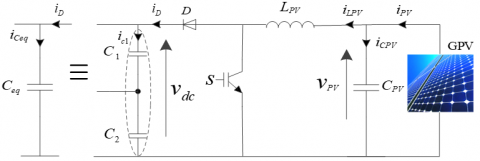
The output of the photovoltaic generator (PVG) is connected to a boost converter, as represented in Figure 2.
Figure 2. Boost converter of the PV generator
The state space model for this converter is represented by the dynamic equations below [14]:
$\begin{align} & \frac{d{{v}_{pv}}}{dt}=\frac{1}{{{C}_{pv}}}{{i}_{pv}}-\frac{1}{{{C}_{pv}}}{{i}_{Lpv}} \\ & \frac{d{{i}_{Lpv}}}{dt}=\frac{1}{{{L}_{pv}}}{{v}_{pv}}-\frac{1}{{{L}_{pv}}}{{v}_{dc}} \\ \end{align}$ (7)
with D is defined as duty cycle, the boost’s average model becomes as follows:
$\begin{align} & \frac{d{{i}_{Lpv}}}{dt}=\frac{1}{{{L}_{pv}}}{{v}_{pv}}-\frac{1}{{{L}_{pv}}}(1-D){{v}_{dc}} \\ & \frac{d{{v}_{pv}}}{dt}=\frac{1}{{{C}_{pv}}}{{i}_{pv}}-\frac{1}{{{C}_{pv}}}(1-D){{i}_{Lpv}} \\ \end{align}$ (8)
The equations can be put in the following form:
${{\dot{x}}_{b}}={{f}_{b}}({{x}_{b}})+{{g}_{b}}({{x}_{b}}){{u}_{b}}$ (9)
where:
$f_{b}\left(x_{b}\right)=\left[\begin{array}{c}\frac{1}{L_{p v}} v_{p v} \\ \frac{1}{C_{p v}} i_{p v}\end{array}\right], g_{b}\left(x_{b}\right)=\left[\begin{array}{cc}-\frac{1}{L_{f p}} & 0 \\ 0 & -\frac{1}{C_{p v}}\end{array}\right]$,
$x_{b}=\left[\begin{array}{c}i_{L p v} \\ v_{p v}\end{array}\right], u_{b}=\left[\begin{array}{c}v_{d c} \\ i_{L p v}\end{array}\right]$
$y_{b}=\left[\begin{array}{l}y_{b 1} \\ y_{b 2}\end{array}\right]=\left[\begin{array}{l}h_{b 1} \\ h_{b 2}\end{array}\right]$
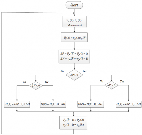
2.2 MPPT detection algorithm
The DC-DC boost converter is commonly utilised in solar PV units, amplifying and regulating the PV panel voltage at a given level while extracting maximum power. The boost converter is controlled by a Maximum Power Point Tracking (MPPT) controller [5].
In this study, the P&O detection algorithm is employed because of its simplicity of use and low-cost implementation [7]. The flowchart of P&O detection algorithm is presented in Figure 3.
The Perturb & Observe algorithm consists of changing the operating point of the PV generator by raising or reducing the duty cycle of the boost converter for the aim of measuring the output power before and after the perturbation. The algorithm perturbs the structure in the same direction as the power increases; otherwise, it perturbs the structure in the reverse direction. As shown in Figure 3, there are four possible options that are presented during the tracking of the MPPT.
2.3 Harmonic identification
The identification strategy used to remove harmonics from perturbed waveforms has a big impact on the performance of the active filter [10, 19]. The methods employed for extracting harmonics are detailed in the following parts.
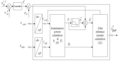
2.3.1 Harmonic currents identification using PQ-theory
The instantaneous power theory technique (PQ theory) is used in this study as illustrated in Figure 4.
The load's instantaneous powers are computed as follows [18]:
$\left[\begin{array}{c}P_{l} \\ Q_{l}\end{array}\right]=\left[\begin{array}{cc}v_{s \alpha} & v_{s \beta} \\ v_{s \beta} & -v_{s \alpha}\end{array}\right]\left[\begin{array}{l}i_{l \alpha} \\ i_{l \beta}\end{array}\right]$ (10)
Figure 3. P&O detection algorithm
Figure 4. Harmonic currents extraction scheme using PQ theory
Figure 5. Harmonic voltages extraction scheme using PQ-PLL theory
The powers could be written in the following way:
$\left\{\begin{array}{l}P_{l}=\bar{P}_{l}+\tilde{P}_{l} \\ Q_{l}=\bar{Q}_{l}+\tilde{Q}_{l}\end{array}\right.$ (11)
For compensating reactive power and mitigating harmonics, the total reactive power ($\bar{Q}_{l}$ and $\widetilde{Q}_{l}$ components) with the oscillatory component of active power are chosen as compensatory power references, then, the compensating currents reference are calculated as in (12).
$\left[\begin{array}{c}i_{f p \alpha}^{*} \\ i_{f p \beta}^{*}\end{array}\right]=\frac{1}{v_{s \alpha}^{2}+v_{s \beta}^{2}}\left[\begin{array}{cc}v_{s \alpha} & v_{s \beta} \\ v_{s \beta} & -v_{s \alpha}\end{array}\right]\left[\begin{array}{c}\tilde{P}_{l} \\ Q_{l}\end{array}\right]$ (12)
2.3.2 Harmonic voltages identification using PQ-PLL theory
It consists of two parts in which the first is to extract voltage harmonics, and it is similar to PQ theory for currents (13).
$\left[\frac{\overline{{\mathcal{V}}_{s \alpha}}}{{\mathcal{V}}_{s \beta}}\right]=\frac{1}{i_{l \alpha}^{2}+i_{l \beta}^{2}}\left[\begin{array}{cc}i_{l \alpha} & i_{l \beta} \\ -i_{l \beta} & i_{l \alpha}\end{array}\right]\left[\begin{array}{l}\overline{P}_{l} \\ \overline{Q_{l}}\end{array}\right]$ (13)
The harmonic voltages are calculated by:
$\left[\begin{array}{l}\mathcal{V}_{h \alpha} \\ \mathcal{V}_{h \beta}\end{array}\right]=\left[\begin{array}{l}\mathcal{V}_{s \alpha} \\ \mathcal{V}_{s \beta}\end{array}\right]-\left[\begin{array}{l}\overline{\mathcal{V}_{s \alpha}} \\\overline{\mathcal{V}_{s \beta}}\end{array}\right]$ (14)
By adding the voltage drop across the load, the reference voltages are given by:
$\left[\begin{array}{c}v_{f s \alpha}^{*} \\ v_{f_{s} \beta}^{*}\end{array}\right]=\left[\begin{array}{c}v_{h \alpha} \\ v_{h \beta}\end{array}\right]+\left[\begin{array}{c}\Delta v_{l \alpha} \\ \Delta v_{l \beta}\end{array}\right]$ (15)
Figure 5 represents the schematic diagram of the PQ-PLL theory.
2.4 Feedback linearisation controller (FLC) synthesis
Consider the nonlinear system represented in:
$\dot{x}=f(x)+\sum_{i=1}^{p} g_{i}(x) u_{i} \quad i=1,2, \ldots, p$
$y_{i}=h_{i}(x)$ (16)
g(x), f(x) and h(x) represent a scalar functions.
The well-known approach for forming the previous system's feedback linearisation law is shown in Figure 6 [20]. The problem of determining the system's vector relative degree (13) necessitates differentiation of each output signal until one of the input signals is explicitly included in the differentiation. We define rj as the minimal integer for each output signal that has one input in $y_{j}^{\left(r_{j}\right)}$ [9]:
$y_{j}^{\left(r_{j}\right)}=L_{f}^{r_{j}} h(x)+\sum_{i=1}^{p} L_{g i}\left(L_{f}^{r_{j}-1} h_{j}(x)\right) u_{i} \quad j=1,2, \ldots, ., p$ (17)
where: $L_{f} h_{j}$ and $L_{g i}\left(L_{f}^{r_{j}-1} h_{j}\right)$ represent the Lie derivatives of h with regard to f and g.
The global relative degree equals to the total of all relative degrees calculated using (13) [21]. It should be less than or equal to the system's order.: $r=\sum_{j=1}^{p} r_{j} \leq n$.
The formula (17) can be represented in its matrix form to obtain the expression of linearising law u that permits making the relationship between inputs and outputs linear [9]:
$\left[\begin{array}{cccc}y_{1}^{r_{j}} & \ldots & \ldots & y_{p}^{r_{p}}\end{array}\right]^{t}=\zeta(x)+D(x) u$ (18)
where:
$\zeta (x)=\left( \begin{align} & {{L}_{f}}^{{{r}_{1}}}{{h}_{1}}(x) \\ & {{L}_{f}}^{{{r}_{2}}}{{h}_{2}}(x) \\ & \text{ }. \\ & \text{ }. \\ & \text{ }. \\ & {{L}_{f}}^{{{r}_{p}}}{{h}_{p}}(x) \\ \end{align} \right)$
And
$D(x)=\left( \begin{align} & {{L}_{{{g}_{1}}}}{{L}_{f}}^{{{r}_{1}}-1}{{h}_{1}}\,\,\,\,\,\,\,{{L}_{{{g}_{2}}}}{{L}_{f}}^{{{r}_{1}}-1}{{h}_{1}}\,\,\,\,\,\,\,.\,\,\,\,\,\,\,.\,\,\,\,\,\,\,.\,\,\,\,\,\,\,.\,\,\,\,\,\,\,{{L}_{{{g}_{p}}}}{{L}_{f}}^{{{r}_{1}}-1}{{h}_{1}} \\ & {{L}_{{{g}_{1}}}}{{L}_{f}}^{{{r}_{2}}-1}{{h}_{2}}\,\,\,\,\,\,{{L}_{{{g}_{2}}}}{{L}_{f}}^{{{r}_{2}}-1}{{h}_{2}}\,\,\,\,\,\,.\,\,\,\,\,\,\,.\,\,\,\,\,\,\,.\,\,\,\,\,\,\,.\,\,\,\,\,\,{{L}_{{{g}_{p}}}}{{L}_{f}}^{{{r}_{2}}-1}{{h}_{2}} \\ & \,\,\,\,\,\,\,\,\,\,\,.\,\,\,\,\,\,\,\,\,\,\,\,\,\,\,\,\,\,\,\,\,\,\,\,\,\,\,\,\,.\,\,\,\,\,\,\,\,\,\,\,\,\,\,\,\,\,.\,\,\,\,\,\,\,.\,\,\,\,\,\,\,.\,\,\,\,\,\,\,.\,\,\,\,\,\,\,\,\,\,\, \\ & {{L}_{{{g}_{1}}}}{{L}_{f}}^{{{r}_{p}}-1}{{h}_{p}}\,\,\,\,{{L}_{{{g}_{2}}}}{{L}_{f}}^{{{r}_{p}}-1}{{h}_{p}}\,\,\,\,\,.\,\,\,\,\,\,\,.\,\,\,\,\,\,\,.\,\,\,\,\,\,\,.\,\,\,\,\,\,{{L}_{{{g}_{p}}}}{{L}_{f}}^{{{r}_{p}}-1}{{h}_{p}} \\ \end{align} \right)$
D(x) is called the decoupling matrix system.
The linearizing control law has the following form [9]:
$u=D{{(x)}^{-1}}(-\zeta (x)+v)$ (19)
It is important to note that linearisation is only possible if the decoupling matrix D(x) is reversible. Figure 6 shows the linearised system's block diagram.
2.4.1 DC-link voltage FLC design
The design of the DC link voltage controller is based on (5). The derivative of the output y=h = vdc2 is computed as:
$\overset{\centerdot }{\mathop{y}}\,={{L}_{f}}h(x)+{{L}_{g}}h(x)u=\frac{2}{{{C}_{dc}}}P_{dc}^{{}}$ (20)
The control Pdc is figured in (20); hence, its relative degree r =1. The relative degree of this output is equal to the order of the system which clearly corresponds to an exact linearisation [10].
The control is then determined by:
$P_{dc}^{*}=\frac{{{C}_{dc}}}{2}v$ (21)
where: $\dot{y}=v$.
For the problem of trajectory tracking defined by vdc*(t), the linearizing control law v is defined by:
$v={{k}_{dc}}(v_{dc}^{{{*}^{2}}}-v_{dc}^{2})+\frac{dv_{dc}^{*2}}{dt}$ (22)
where, kdcis a positive constant.
2.4.2 Parallel currents FLC design
Each output derivative is given by:
${{\dot{y}}_{j}}={{L}_{f}}^{{}}h(x)+\sum\limits_{i=1}^{2}{{{L}_{gi}}({{L}_{f}}^{{}}{{h}_{j}}(x))}{{u}_{i}}\,\,\,j=1,2\,$ (23)
Then, the matrix form of (23) can be expressed as:
$\left[\begin{array}{c}\dot{y}_{p 1} \\ \dot{y}_{p 2}\end{array}\right]=\left[\begin{array}{c}-\frac{R_{f p}}{L_{f p}} x_{p 1} \\ -\frac{R_{f p}}{L_{f p}} x_{p 2}\end{array}\right]+\left[\begin{array}{cc}\frac{1}{L_{f p}} & 0 \\ 0 & \frac{1}{L_{f p}}\end{array}\right]\left[\begin{array}{l}u_{p 1} \\ u_{p 2}\end{array}\right]$ (24)
The decoupling matrix is reversible (det(Dp(x)) ≠0), then the linearizing control law can be given as:
$u_{p}=\left[\begin{array}{l}u_{p 1} \\ u_{p 2}\end{array}\right]=D_{p}\left(x_{p}\right)^{-1}\left[-\zeta_{p}\left(x_{p}\right)+\left[\begin{array}{l}v_{p 1} \\ v_{p 2}\end{array}\right]\right]$ (25)
By applicating the linearisation law, we obtain the following decoupled linear system:
$\left[\begin{array}{l}\dot{y}_{p 1} \\ \dot{y}_{p 2}\end{array}\right]=\left[\begin{array}{c}v_{p 1} \\ v_{p 2}\end{array}\right]$ (26)
Figure 6. Block diagram of linearised MIMO system
The control law utilised for tracking the current reference is:
$v_{p 1}=k_{p 1}\left(i_{f p \alpha}^{*}-i_{f p \alpha}\right)+\frac{d i_{f p \alpha}^{*}}{d t}$
$v_{p 2}=k_{p 2}\left(i_{f p \beta}^{*}-i_{f p \beta}\right)+\frac{d i_{f p \beta}^{*}}{d t}$ (27)
where, kp1 and kp2are positive constants.
From (25) and (27), the control law is given by:
$v_{f p \alpha}^{*}=R_{f p} i_{f p \alpha}+v_{s \alpha}+L_{f p}\left(k_{p 1}\left(i_{f p \alpha}^{*}-i_{f p \alpha}\right)+\frac{d i_{f p \alpha}^{*}}{d t}\right)$
$v_{f p \beta}^{*}=R_{f p} i_{f p \beta}+v_{s \beta}+L_{f p}\left(k_{p 2}\left(i_{f p \beta}^{*}-i_{f p \beta}\right)+\frac{d i_{f p \beta}^{*}}{d t}\right)$ (28)
2.4.3 Series currents FLC design
Each output derivative is given by:
$\dot{y}_{j}=L_{f} h(x)+\sum_{i=1}^{2} L_{g i}\left(L_{f} h_{j}(x)\right) u_{i} \quad j=1,2$ (29)
Then, (29) can be written in the matrix form as:
$\left[\begin{array}{l}\dot{y}_{s 1} \\ \dot{y}_{s 2}\end{array}\right]=\left[\begin{array}{c}-\frac{R_{f s}}{L_{f s}} x_{s 1} \\ -\frac{R_{f s}}{L_{f s}} x_{s 2}\end{array}\right]+\left[\begin{array}{cc}\frac{1}{L_{f s}} & 0 \\ 0 & \frac{1}{L_{f s}}\end{array}\right]\left[\begin{array}{l}u_{s 1} \\ u_{s 2}\end{array}\right]$ (30)
The decoupling matrix is reversible (det(Ds(x)) ≠0), then the linearizing control law can be given as:
$u_{s}=\left[\begin{array}{l}u_{s 1} \\ u_{s 2}\end{array}\right]=D_{s}(x)^{-1}\left[-\zeta_{s}(x)+\left[\begin{array}{l}v_{s 1} \\ v_{s 2}\end{array}\right]\right]$ (31)
By applying the linearisation law, we obtain the following decoupled linear system:
$\left[\begin{array}{l}\dot{y}_{s 1} \\ \dot{y}_{s 2}\end{array}\right]=\left[\begin{array}{l}v_{s 1} \\ v_{s 2}\end{array}\right]$ (32)
The control law utilized for tracking the voltage reference is:
$v_{s 1}=k_{s 1}\left(i_{f s \alpha}^{*}-i_{f s \alpha}\right)+\frac{d i_{f s \alpha}^{*}}{d t}$
$v_{s 2}=k_{s 2}\left(i_{f s \beta}^{*}-i_{f s \beta}\right)+\frac{d i_{f s \beta}^{*}}{d t}$ (33)
where, ks1 and ks2are positive constants.
From (31) and (33), the control law is given by:
$v_{f s \alpha}^{*}=R_{f s} i_{f s \alpha}+v_{i n j \alpha}+L_{f s}\left(k_{s 1}\left(i_{f s \alpha}^{*}-i_{f s \alpha}\right)+\frac{d i_{f s \alpha}^{*}}{d t}\right)$
$v_{f s \beta}^{*}=R_{f s} i_{f s \beta}+v_{i n j \beta}+L_{f s}\left(k_{s 2}\left(i_{f s \beta}^{*}-i_{f s \beta}\right)+\frac{d i_{f s \beta}^{*}}{d t}\right)$ (34)
2.4.4 Boost FLC design
Each output derivative is given by:
$\dot{y}_{j}=L_{f} h(x)+\sum_{i=1}^{2} L_{g i}\left(L_{f} h_{j}(x)\right) u_{i} \quad j=1,2$ (35)
Then, the matrix form of (35) can be expressed as:
$\left[\begin{array}{l}\dot{y}_{b 1} \\ \dot{y}_{b 2}\end{array}\right]=\left[\begin{array}{l}\frac{1}{L_{p v}} x_{b 1} \\ \frac{1}{C_{p v}} x_{b 2}\end{array}\right]+\left[\begin{array}{cc}-\frac{1}{L_{p v}} & 0 \\ 0 & -\frac{1}{C_{p v}}\end{array}\right]\left[\begin{array}{l}u_{b 1} \\ u_{b 2}\end{array}\right]$ (36)
The decoupling matrix is reversible (det(Db(x)) ≠0), then the linearizing control law can be given as:
$u_{b}=\left[\begin{array}{l}u_{b 1} \\ u_{b 2}\end{array}\right]=D_{b}\left(x_{b}\right)^{-1}\left[-\zeta_{b}\left(x_{b}\right)+\left[\begin{array}{l}v_{b 1} \\ v_{b 2}\end{array}\right]\right]$ (37)
By applying the linearisation law, we obtain the following decoupled linear system:
$\left[\begin{array}{l}\dot{y}_{b 1} \\ \dot{y}_{b 2}\end{array}\right]=\left[\begin{array}{l}v_{b 1} \\ v_{b 2}\end{array}\right]$ (38)
The control law utilized for tracking the reference is:
$v_{b 1}=k_{b 1}\left(i_{L p v}^{*}-i_{L p v}\right)+\frac{d i_{L p v}^{*}}{d t}$
$v_{b 2}=k_{b 2}\left(v_{p v}^{*}-v_{p v}\right)+\frac{d v_{p v}^{*}}{d t}$ (39)
where, kb1 and kb2are positive constants.
From (37) and (38), the control law is given by:
$v_{d c}^{*}=v_{p v}+L_{p v}\left(k_{b 1}\left(i_{L p v}^{*}-i_{L p v}\right)+\frac{d i_{L p v}^{*}}{d t}\right)$
$i_{L p v}^{*}=i_{p v}+C_{p v}\left(k_{b 2}\left(v_{p v}^{*}-v_{p v}\right)+\frac{d v_{p v}^{*}}{d t}\right)$ (40)
2.5 Space vector modulation
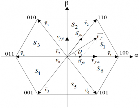
In this part, the space vector modulation (SVM) algorithm is described to produce the switches PWM control signals (sa, sb and sc) [22]. The SVM schematic of a 3-phase IGBT-based voltage source inverter is a hexagon (Figure 7), constituted of six sectors. Each sector is an equilateral triangle of a height h =√3/2 [23]. The sector of operation to every given reference vector is obtained using Eq. (41).
$S_{i}=\operatorname{int}\left(\frac{\theta_{s}}{60}\right)+1$ (41)
Figure 7. SVM diagram
All sectors use the same on-time calculation. The following is the volt-second equation [24]:
$\overrightarrow{v_{f}} T_{s}=t_{i} \vec{v}_{i}+t_{i+1} \vec{v}_{i+1}+t_{0} \vec{v}_{0}$ (42)
where, fs: switching frequency, with Ts=1/fs.
In sector 1,
$\left\{\begin{array}{l}\vec{v}_{1}=\sqrt{\frac{2}{3}} v_{d c} \\ \vec{v}_{2}=\sqrt{\frac{2}{3}} v_{d c}\left(\frac{1}{2}+j \frac{\sqrt{3}}{2}\right) \\ \vec{v}_{0}=0\end{array}\right.$ (43)
The reference to be regenerated could also be expressed as follows,
$\overrightarrow{v_{f}}=v_{f \alpha}+j v_{f \beta}$ (44)
Eqns. (42)-(44) can be used to get:
$\left\{\begin{array}{l}v_{f \alpha}=\sqrt{\frac{2}{3}} v_{d c} \frac{t_{1}}{T_{s}}+\frac{1}{\sqrt{6}} v_{d c} \frac{t_{2}}{T_{s}} \\ v_{f \beta}=\frac{1}{\sqrt{2}} v_{d c} \frac{t_{2}}{T_{s}}\end{array}\right.$ (45)
Finally, the ON-times are calculated using Eq. (45) [25].
$\left\{\begin{array}{l}t_{1}=\frac{\sqrt{6} v_{f \alpha}-\sqrt{2} v_{f \beta}}{v_{d c}} T_{s} \\ t_{2}=\frac{\sqrt{2} v_{f \beta}}{v_{d c}} T_{s} \\ t_{0}=T_{s}-\left(t_{1}+t_{2}\right)\end{array}\right.$ (46)
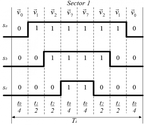
The SVM scheme is determined by which null vector is used.
There are three options: only use the null vector v0, only use the null vector v7, or use a combination of null vectors. Altering the null vector of every cycle and reversing the sequence after every null vector is a popular SVM approach as shown in Figure 8. This is what we'll call it, the symmetric 7-segment approach [24].
Figure 8. 7-segment switching sequence for Vref in sector
2.6 Comparative PI controller design
The suggested FL-SVM's performance is compared with that of the PI controller to illustrate its efficiency. As shown below, the design of the PI controller is detailed.
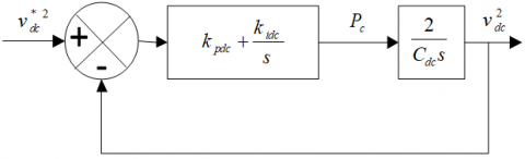
The role of the DC PI controller is to allow tracking the reference by controlling the active power flow between the PCC and the DC bus [26].
From Eq. (5), the following transfer function is calculated:
$\frac{v_{d c}^{2}(s)}{P_{c}(s)}=\frac{2}{C_{d c} s}$ (47)
Figure 9 shows a closed - loop schematic of DC voltage regulation.
Figure 9. DC voltage regulation
The closed loop transfer function is given in:
$G(s)=\frac{v_{d c}^{2}(s)}{v_{d c}^{* 2}(s)}=\frac{\frac{2 k_{p d c}}{C_{d c}} s+\frac{2 k_{i d c}}{C_{d c}}}{s^{2}+\frac{2 k_{p d c}}{C_{d c}} s+\frac{2 k_{i d c}}{C_{d c}}}$ (48)
By the identification of (48) to a second order canonic transfer function (49):
$H(s)=\frac{2 \zeta \omega_{n} s+\omega_{n}^{2}}{s^{2}+2 \zeta \omega_{n} s+\omega_{n}^{2}}$ (49)
We can find:
$k_{i d c}=C_{d c} \omega_{n}^{2} / 2$
$k_{p d c}=\xi \omega_{n} C_{d c}$ (50)
$\omega_{n}=2 \pi f_{n}$ is the Natural pulsatance of the controller, and 0<ξ<1 is the damping factor for a good dynamic and acceptable oscillations, we choose $f_{n}=25 H z \xi=0.7$.
By the same method, we can also obtain the PI coefficients of currents, voltages and Boost controllers as summarized in Table 1.
Table 1. PI parameters
|
Coefficients |
Value |
|
kpdc |
0.7*2*3.14*25*0.008= 0.88 |
|
Kidc |
0.1 |
|
kpfp |
3.5 |
|
Kifp |
355 |
|
kpfs |
0.3 |
|
Kifs |
10 |
|
Kppv |
0.45 |
|
Kipv |
4.6 |
2.7 Principle of PIL co-simulation
Prototyping "Processor in the Loop" has the advantage of validating the digital implementation of control algorithms in the control part while the computer emulates the power part. It is therefore possible to evaluate the control part in a virtual environment where adjustments in the control algorithms are easily achieved by reprogramming without costly hardware iteration. The latter results in a minimisation in development’s time, as well as cost of the project.
Controlling the suggested PVG-UPQC system in the Simulink.
Platform using the generated control algorithm embedded in STM32F429I-DISC DSP board, as illustrated in Figure 10.
2.8 The PIL implementation technique steps of the control algorithms
In PIL co-simulation, an embedded platform running the control algorithm is connected to a host computer on which the physical system model is executed. Then, an evaluation of the execution circumstances of the developed algorithm can be performed in order to optimize some important factors such as memory footprint, code size and execution of the algorithm according to the required time.
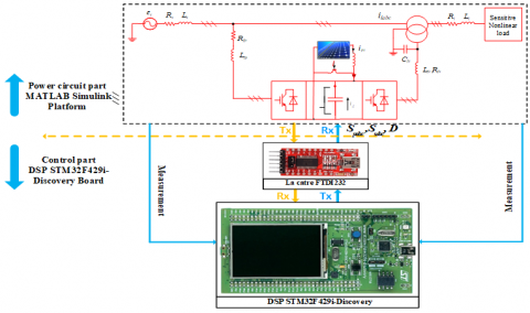
During PIL prototyping, at each simulation step, the power part of the electrical system is simulated in the Matlab / Simulink platform and the output signals are sent to the STM32F429i-Discovery DSP board. When it receives the signals from the standard PC, it executes the implemented control algorithms. The DSP board then sends back to the PC the control commands to the electrical system simulated in the Matlab / Simulink platform. At this stage, a PIL simulation cycle is done. The exchange of data between the standard PC and the DSP board is synchronized using an FTDI232 interface (serial communication) to connect the DSP board to the standard PC as indicated in Figure 10. To do so, we need to achieve the following steps:
Figure 10. The structure of the PIL co-simulation
Phase I:
The objective of this step is to generate the C code for all the control algorithms of the system.
Step 01:
Simulation of the system using the Embedded Matlab Function.
Phase II:
The PIL co-simulation is performed between the DSP board and the Simulink MATLAB platform. The implementation of the PIL procedure with existing resources is as follows:
Step 01:
-Grouping of all the control algorithms of the proposed system in a single simulation subsystem,
Step 02:
-Define the reference of the DSP board in the Simulink Matlab platform and define the appropriate inputs and outputs of the control system. After that, the proposed control algorithm will be built and integrated into the DSP board,
Step 03:
-Select a communication interface between the DSP board and the Simulink platform,
Step 04:
-Set the appropriate time step in Simulink according to the application,
Step 05:
-Download the compiled algorithm control model of the entire subsystem to be incorporated into the DSP board,
Step 06:
-Configure and control the proposed system on the Simulink Matlab platform using the control algorithm embedded in the DSP board.
Harmonic current and voltage filtering, reactive power compensation and performance evaluation of the PVG-UPQC with the suggested controller have been analysed in Matlab/Simulink environment under nonlinear load variation and voltage sag/swell. The parameters of the system used in this study are presented in Table 2.
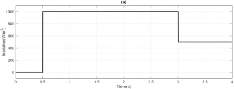
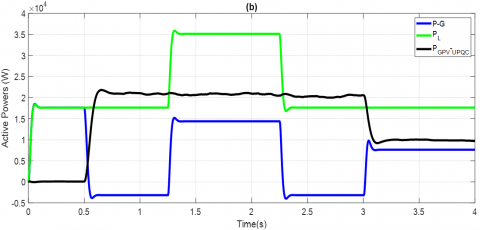
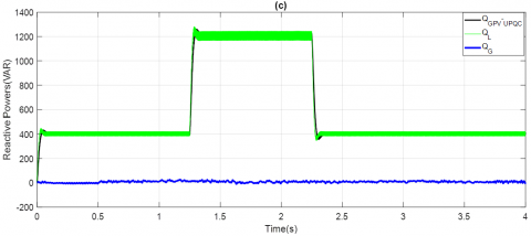
Figure 11 (a) illustrates the selected irradiation’s profile when the temperature is adjusted to 25℃. Initially, there is no irradiation (t<0.5s), the PVG-UPQC is controlled just to filtrate harmonics and compensate reactive power, while the load is fed by the grid (17.5 kW). Then, irradiation is adjusted to reach 1000 W/m2, in this case the injected maximum power is about 21 kW and the produced power is higher than the power required by the load, so the PVG-UPQC is controlled to filtrate harmonics, compensate reactive power, feed the load and inject power to the grid between [t =0.5s and t =1.25s] (see Figure 11 (b) and (c)). From these figures, it is obvious that throughout the simulation, the consumed active and reactive powers (respectively 17.5 kW and 400 VAR) are equal to the sum of those delivered by the PVG-UPQC and the grid.
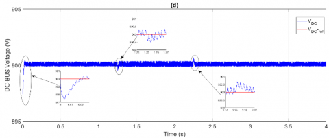
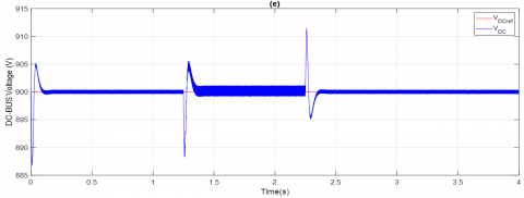
The load variation has a negligible effect on the DC-link voltage (about 2V), and it recovers in around 0.06s (see Figure 11 (d)).
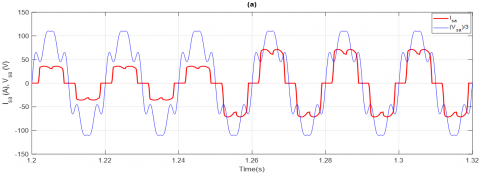
The dynamic behavior under an abrupt variation of load, by adding another load having the same value between [t =1.25s and t =2.25s] which is illustrated in Figures 12.a and 12.b. It is clear to see that the grid current, after applying the control, is pure sinusoidal, moreover, even in this temporary state, the unity power factor goal is successfully reached.
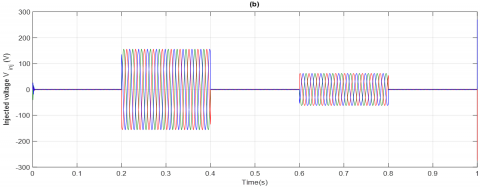
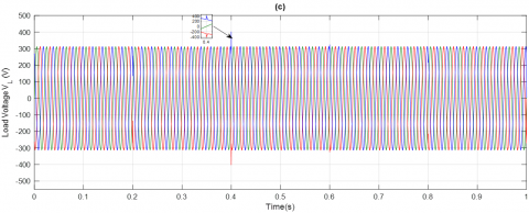
From the sag and swell tests illustrated in Figures 13.a and 13.b, it can be observed that the PVG-UPQC quickly injects equal positive voltage components in the case off sag which are phase-locked to the grid voltage, while in the case of voltage swell, the PVG-UPQC inject negative voltage components in opposite phase with grid voltage to correct and maintain the load voltage close to its normal value (see Figure 13.c).
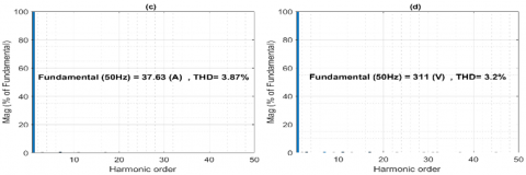
In case of feedback control, the spectral analysis of AC grid current and the voltage of the load with and without compensation are presented in Figure 12. (c) and (d), for current in Figure 12. (g) and (h) for voltage. For linear control, the same spectrums are shown in Figure 14 (c) and (d). It reveals that the UPQC decreases THD in the grid currents from 28.11% to 3.87% with the classic PI controller. whilst, with feedback linearisation based SVM controller, the current THD is decreased to 2.30%. The load voltage THD decreases from 24.59% to 3.2% with PI, while it is further decreased to 1.94% when feedback linearisation based SVM controller is applied which demonstrates the efficiency of the developed nonlinear controller.
With the view to validate the robustness and reliability of the proposed PVG-UPQC system, a test with a sag and swell in the grid voltage has been carried out. As we can depict in the Figure 13, the load voltage was again found quickly very close to a sinusoidal voltage under sag and swell voltages variations. So, the PVG-UPQC is capable to deliver the required compensating voltage components to keep constant load voltage.
The absence of an overshoot in DC bus voltage response during load variation, rapidity and negligible THD, proves the superiority and the effectiveness of the feedback linearization based SVM controller compared to the traditional linear PI controller as presented in Table 3.
Table 2. System parameters
|
Parameter |
value |
|
RMS value of the source voltage |
220 V |
|
DC-link capacitor Cdc |
8 mF |
|
Source impedance Rs, Ls |
3mΩ, 2.6 μH |
|
Shunt filter impedance Rfp, Lfp |
20 mΩ, 2.5 mH |
|
Series filter impedance Rfs, Lfs,Cfs |
1.5 Ω, 3 mH, 0.1 mF |
|
boost converter parameters Lpv,Cpv |
5 mH, 55 mF |
|
Line impedance Rl, Ll |
10 mΩ, 0.3 μH |
|
Diode rectifier load Rd, Ld |
15 Ω, 2 mH |
|
PV array Ppv, Vmp,Imp, Isc,Voc |
150W,34.5V,4.35A.4.75A, 43.5V |
|
DC-link voltage reference |
900 V |
|
Switching frequency fs |
12 kHz |
|
kp1= kp2 |
1120 |
|
ks1= ks2 |
1150 |
|
Kb1= kb2 |
1450 |
|
kdc |
250 |
Table 3. Comparison of PI controller with FL-SVM
|
Factor |
PI controller |
FL-SVM controller |
|
THDi (%) |
3.87 |
2.30 |
|
THDv (%) |
3.2 |
1.94 |
|
Charging of DC link (s) |
0.11 |
0.06 |
|
Overshoot |
+ |
- |
Figure 11. Simulation results under weather variation of the suggested controller. a): Variations of irradiations, b): Active power exchange of the PVG-UPQC under weather variations, c): Reactive power exchange of the PVG-UPQC under weather variations, d): DC-link voltage vdc
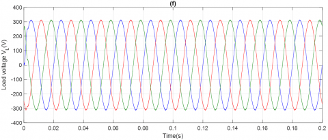
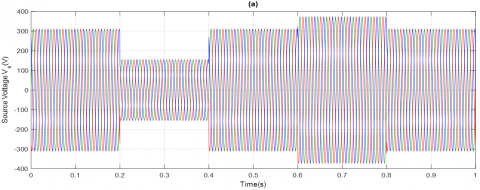
Figure 12. Simulation results under load variation of the suggested controller. a): A-phase source voltage with source current before compensation, b): A-phase source voltage with source current after compensation, c): Source current harmonic spectrum before compensation, d): Source current harmonic spectrum after compensation, e): Voltage of the load before compensation. f): Voltage of the load after compensation. g): Harmonic spectrum of load voltage before compensation, h): Load voltage harmonic spectrum after compensation
Figure 13. Simulation results during a sag and a swell test of the suggested controller. a): Perturbed source voltage profile. b): Compensation voltage during perturbation. c): Voltage of the load after compensation
Figure 14. Simulation results with PI controller. a): A-phase source voltage with source current after compensation, b): Voltage of the load after compensation. c): Source current harmonic spectrum after compensation, d): Load voltage harmonic spectrum after compensation. e): DC bus voltage vdc
This paper has attained a control design of the PVG-UPQC in addition to its mathematical model and harmonic extraction methods for both currents and voltages. Additionally, Feedback linearisation combined with SVM controller technique is derived to suppress currents and voltages harmonics in the grid. A two-level SVM technique were used due to its benefits in terms of a fixed frequency implementation. Co-simulation results based on the PIL technique has been fulfilled in all stages the system operation under nonlinear load changes and voltage sag/swell as well. The results shown in this paper has clearly proves the superiority and the robustness of the proposed controller of the PVG-UPQC, and offers much better performance compared to the traditional PI controller. Otherwise, in the future, to suppress the limitations of the injected power, the system will be implemented with more kilo watts delivered to the grid in addition to involve real practical implantations instead of PIL technique.
|
Xfp |
X related to the parallel filter |
|
Xfs |
X related to the series filter |
|
P |
Active Power (W) |
|
Q |
Reactive Power (VAR) |
|
i |
Electrical Current (A) |
|
v |
Electrical Voltage (V) |
|
Abbreviation |
|
|
PVG |
Photo Voltaic Generator |
|
UPQC |
Unified Power quality Conditioner |
|
SVM |
Space Vector Modulation |
|
DC |
Direct Current |
|
FL |
Feedback Linearisation |
|
THD |
Total Harmonic Distortion |
|
MPPT |
Maximum Power Point Tracking Algorithm |
|
P&O |
perturb & Observe algorithm |
[1] Gongati, P.R.R., Marala, R.R., Malupu, V.K. (2020). Mitigation of certain power quality issues in wind energy conversion system using UPQC and IUPQC devices. European Journal of Electrical Engineering, 22(6): 447-455. https://doi.org/10.18280/ejee.220606
[2] Kumar, P. (2020). Power quality investigation by reduced switching UPQC. European Journal of Electrical Engineering, 22(4-5): 335-347. https://doi.org/10.18280/ejee.224-505
[3] De Silva, H.J., Shafieipour, M. (2021). An improved passivity enforcement algorithm for transmission line models using passive filters. Electric Power Systems Research, 196: 107255. https://doi.org/10.1016/j.epsr.2021.107255
[4] Patnaik, N., Panda, A.K. (2016). Performance analysis of a 3 phase 4 wire UPQC system based on PAC based SRF controller with real time digital simulation. International Journal of Electrical Power & Energy Systems, 74: 212-221. https://doi.org/10.1016/j.ijepes.2015.07.027
[5] Gurrola-Corral, C., Segundo, J., Esparza, M., Cruz, R. (2020). Optimal LCL-filter design method for grid-connected renewable energy sources. International Journal of Electrical Power & Energy Systems, 120: 105998. https://doi.org/10.1016/j.ijepes.2020.105998
[6] Hemalatha, R., Ramasamy, M. (2020). Microprocessor and PI controller based three phase CHBMLI based DSTATCOM for THD mitigation using hybrid control techniques. Microprocessors and Microsystems, 76: 103093. https://doi.org/10.1016/j.micpro.2020.103093
[7] Bacon, V.D., da Silva, S.A.O., Guerrero, J.M. (2022). Multifunctional UPQC operating as an interface converter between hybrid AC-DC microgrids and utility grids. International Journal of Electrical Power & Energy Systems, 136: 107638. https://doi.org/10.1016/j.ijepes.2021.107638
[8] Dahdouh, A., Barkat, S., Chouder, A. (2016). A combined sliding mode space vector modulation control of the shunt active power filter using robust harmonic extraction method. Algerian Journal of Signals and Systems, 1(1): 37-46. https://doi.org/10.51485/ajss.v1i1.17
[9] Benaissa, A., Bouzidi, M., Barkat, S. (2012). Application of feedback linearization to the virtual flux direct power control of three-level three-phase shunt active power filter. International Review on Modelling and Simulations, 5(3).
[10] Koroglu, T., Tan, A., Savrun, M.M., Cuma, M.U., Bayindir, K.C., Tumay, M. (2019). Implementation of a novel hybrid UPQC topology endowed with an isolated bidirectional DC–DC converter at DC link. IEEE Journal of Emerging and Selected Topics in Power Electronics, 8(3), 2733-2746. https://doi.org/10.1109/JESTPE.2019.2898369
[11] Yang, R.H., Jin, J.X. (2020). Unified power quality conditioner with advanced dual control for performance improvement of DFIG-based wind farm. IEEE Transactions on Sustainable Energy, 12(1): 116-126. https://doi.org/10.1109/TSTE.2020.2985161
[12] Mansor, M.A., Hasan, K., Othman, M.M., Noor, S.Z.B.M., Musirin, I. (2020). Construction and performance investigation of three-phase solar PV and battery energy storage system integrated UPQC. IEEE Access, 8: 103511-103538. https://doi.org/10.1109/ACCESS.2020.2997056
[13] Yu, J., Xu, Y., Li, Y., Liu, Q. (2020). An inductive hybrid UPQC for power quality management in premium-power-supply-required applications. IEEE Access, 8: 113342-113354. https://doi.org/10.1109/ACCESS.2020.2999355
[14] Poongothai, S., Srinath, S. (2020). Power quality enhancement in solar power with grid connected system using UPQC. Microprocessors and Microsystems, 79: 103300. https://doi.org/10.1016/j.micpro.2020.103300
[15] Rao, K.S.R., Hong, L.T. (2012). Microcontroller-based variable speed drive for three-phase induction motor in cooling applications. Journal of Energy and Power Engineering, 6(4).
[16] Gade, A.A., Karande, K.J., Jagadale, A.B. (2015). Space vector modulation based feed control using three phase induction motor. International Journal of Modern Trends in Engineering and Research, 2(7): 44-46.
[17] Jose, J., Aruna, T.A. (2014). Space vector modulated quasi z-source inverter for photovoltaic application. International Journal of Electrical Engineering and Technology, 5: 100-110.
[18] Ozdemir, A., Ozdemir, Z. (2014). Digital current control of a three-phase four-leg voltage source inverter by using PQR theory. IET Power Electronics, 7(3): 527-539. https://doi.org/10.1049/iet-pel.2013.0254
[19] Czarnecki, L.S. (2014). Constraints of instantaneous reactive power PQ theory. IET Power Electronics, 7(9): 2201-2208. http://dx.doi.org/10.1049/iet-pel.2013.0579
[20] Bharathi, S.L.K., Selvaperumal, S. (2020). MGWO-PI controller for enhanced power flow compensation using unified power quality conditioner in wind turbine squirrel cage induction generator. Microprocessors and Microsystems, 76: 103080. https://doi.org/10.1016/j.micpro.2020.103080
[21] Dash, S.K., Ray, P.K. (2020). A new PV-open-UPQC configuration for voltage sensitive loads utilizing novel adaptive controllers. IEEE Transactions on Industrial Informatics, 17(1): 421-429. https://doi.org/10.1109/TII.2020.2986308
[22] Guzman, R., de Vicuna, L.G., Morales, J., Castilla, M., Matas, J. (2015). Sliding-mode control for a three-phase unity power factor rectifier operating at fixed switching frequency. IEEE Transactions on Power Electronics, 31(1): 758-769. https://doi.org/10.1109/TPEL.2015.2403075
[23] Chebabhi, A., Fellah, M.K., Benkhoris, M.F., Kessal, A. (2015). Sliding mode controller for four leg shunt active power filter to eliminating zero sequence current, compensating harmonics and reactive power with fixed switching frequency. SJEE, 12(2): 205-218. https://doi.org/10.2298/SJEE1502205C
[24] Ibrahim, Z.B., Hossain, M.L., Bugis, I.B., Lazi, J.M., Yaakop, N.M. (2014). Comparative analysis of PWM techniques for three level diode clamped voltage source inverter. International Journal of Power Electronics and Drive Systems, 5(1): 15. http://dx.doi.org/10.11591/ijpeds.v4i5.6038
[25] Han, J., Li, X., Jiang, Y., Gong, S. (2020). Three-phase UPQC topology based on quadruple-active-bridge. IEEE Access, 9: 4049-4058. https://doi.org/10.1109/ACCESS.2020.3047961
[26] Reisi, A.R., Moradi, M.H., Showkati, H. (2013). Combined photovoltaic and unified power quality controller to improve power quality. Solar Energy, 88: 154-162. https://doi.org/10.1016/j.solener.2012.11.024