Yuxin Li* | Hongli Jing | Fenjun Liu | Zengsheng Li
© 2022 IIETA. This article is published by IIETA and is licensed under the CC BY 4.0 license (http://creativecommons.org/licenses/by/4.0/).
OPEN ACCESS
To optimize the heat dissipation performance of microelectronic equipment, optical instrument, and optoelectronic devices, it’s necessary to explore the heat transfer mechanism of the nanostructure in them, however, due to the limitation of the research objects, there isn’t a uniform simulation method for the thermo-physical properties of such nanostructure. Therefore, this paper aims to study the thermo-physical properties of nanostructure in microelectronic equipment. At first, by structuring Si super lattice nanowires in a specific direction and then using the Ge atoms to replace the Si atoms in the nanowires, this paper built a model for the periodic Si/Ge super lattice nanowires. Then, this paper performed integral operation on the dynamic equations of the two types of atoms using the time integration algorithm to attain the trajectories of Si and Ge atoms in the nanowire structure of the microelectronic equipment, and discussed the influence of the size and geometrical shape of the cross section of nanowires on thermal conductivity. After that, this paper simulated the structure of the nano-scale SiC material, selected appropriate cut-off radius, and optimized the structure of the nanostructure model based on the Discover Minimization module. At last, the thermal conductivity of the nanostructure was calculated and its thermo-physical properties were analyzed.
Nanostructure, thermo-physical property, microelectronic equipment, thermal conductivity
Nanostructure has very a good application prospect in microelectronic devices and have received wide attention from field scholars around the globe in recent years [1-10]. With the development of modern electronic equipment, the design of such equipment develops toward the directions of highly integrated and multifunctional, and the heat dissipation problem during operation rises consequently [11-14]. If the heat of the electronic equipment cannot dissipate in a timely manner, it’ll affect the performance of the equipment and even cause thermal damage to it [15-21]. To optimize the heat dissipation performance of microelectronic equipment, optical instrument, and optoelectronic devices, it’s necessary to explore the heat transfer mechanism of the nanostructure in them, design new materials and new-type devices for energy conversion and utilization that could meet the heat dissipation requirements of electronic equipment, and figure out the laws of specific data changes.
Saleem et al. [22] analyzed the influence of CNS on the thermal conductivity and mechanical properties of SiCw/Si3N4 composites, and the results showed that the thermal conductivity and mechanical properties of SiCw/Si3N4 composites increased with the addition of CNS, their work provided a useful method for manufacturing high-performance multifunctional composites used in the new-type miniature electronic equipment. Scholar Nakamura [23] designed two different nanostructures, one is connected Si nanodots (NDs) with the same crystal orientation, the other is Si films containing epitaxially grown Ge NDs. This work offers a methodology for the independent control of electron and phonon transport using nanostructured materials, which can provide thermo-electric Si-based materials that are compatible with large scale integrated circuit processing technologies. Juraev and Juraeva [24] pointed out that the transfer of heat through nanostructures differs significantly from the corresponding processes inside macroscopic bodies. Various research methods, both theoretical and experimental, are applied to such objects. They proposed an approach to nanostructures with great advantages, attained hyperbolic equations for describing the wave process of thermal signal flow and the properties of heat transfer in nanostructures across a thin layer, in which the simplest task was to determine the thermal conductivity.
World field scholars adopted different modelling methods to analyze and predict the thermal conductivity of nanostructure and nanofluid. However, due to the limitation of the research objects, there isn’t a uniform simulation method for the thermal and physical properties of such nanostructure. Therefore, this paper aims to study the thermo-physical properties of nanostructure in microelectronic equipment. In the second chapter, by structuring Si super lattice nanowires in a specific direction and then using the Ge atoms to replace the Si atoms in the nanowires, this paper built a model for the periodic Si/Ge super lattice nanowires. In the third chapter, this paper performed integral operation on the dynamic equations of the two types of atoms using the time integration algorithm to attain the trajectories of Si and Ge atoms in the nanowire structure of the microelectronic equipment, and discussed the influence of the size and geometrical shape of the cross section of nanowires on thermal conductivity. Then in the fourth chapter, this paper simulated the structure of the nano-scale SiC material, selected appropriate cut-off radius, and optimized the structure of the nanostructure model based on the Discover Minimization module. At last, the thermal conductivity of the nanostructure was calculated and its thermo-physical properties were analyzed.
As mature semiconductor materials, Si and Ge elements are widely used in the manufacturing of integrated circuits and transistors in microelectronic equipment. Table 1 compares the properties of Si, Ge and their alloy.
Table 1. Properties of Si, Ge and their alloy
|
Parameter |
Si |
Ge |
Si1-xGex |
|
Lattice constant |
0.574 |
0.51 |
/ |
|
Density |
2.74 |
5.48 |
2.41~5.84 |
|
Melting point |
1253 |
1363 |
1623~1985 |
|
Debye temperature |
695 |
374 |
317~685 |
|
Band gap |
1.30 |
0.68 |
0.62~1.47 |
|
Electron mobility |
84~1425 |
141~3295 |
5.84 |
|
Hole mobility |
32~369 |
42~2741 |
5.92 |
In this study, the nanowire structure in microelectronic equipment is composed of Si and Ge atoms. Because the strain caused by lattice mismatch at the interface between the two types of atoms is relatively small, so under the premise that the relaxation process is sufficient enough, the influence of lattice mismatch can be ignored when calculating the thermal conductivity of the nanostructure. At first, this paper structured Si super lattice nanowires in a specific direction. The length of nanowires here refers to the total length of the sample, and the shape of the cross-section is a specific geometry. Then, Si atoms in the nanowires were replaced by Ge atoms to build the periodic Si/Ge super lattice nanowire model.
The thermal conductivity of the constructed nanowire model was calculated using a non-equilibrium molecular dynamics simulation method in software LAMMPS, and the interaction force between Si and Ge atoms was described by a Tersoff potential function. Assuming: Oi represents the potential of the i-th atom; Oij represents the interaction energy between the i-th and the j-th atoms; gT and gA respectively represent the repulsion and attraction; i, j, and l represent atoms in the system; tij represents the bond length of ij bond; ωijl represents the bond angle between ij bond and il bond, then the expression for the Tersoff potential function is:
$O=\sum\limits_{i}{{{O}_{i}}}=\frac{1}{2}\sum\limits_{i\ne j}{{{U}_{ij}}}$ (1)
${{U}_{ij}}={{g}_{D}}\left( {{t}_{ij}} \right)\left[ {{g}_{T}}\left( {{t}_{ij}} \right)+{{\phi }_{ij}}{{g}_{X}}\left( {{t}_{ij}} \right) \right]$ (2)
${{g}_{T}}\left( {{t}_{ij}} \right)=-{{X}_{ij}}exp\left( -{{\mu }_{ij}}{{t}_{ij}} \right)$ (3)
${{g}_{X}}\left( {{t}_{ij}} \right)=-{{Y}_{ij}}exp\left( -{{\theta }_{ij}}{{t}_{ij}} \right)$ (4)
Assuming: X, Y, μ, and θ are parameters in the potential function; Tij represents the distance between atoms i and j; Pij represents cut-off radius of potential energy, then the expression of the smooth section function gD is:
${{g}_{D}}=\left\{ \begin{align} & 1,{{t}_{ij}}<{{T}_{ij}} \\ & \frac{1}{2}+\frac{1}{2}cos\left[ \pi \left( {{t}_{ij}}-{{T}_{ij}} \right)/\left( {{P}_{ij}}-{{T}_{ij}} \right) \right],{{T}_{ij}}<{{t}_{ij}}<{{P}_{ij}} \\ & 0,{{t}_{ij}}>{{P}_{ij}} \\\end{align} \right.$ (5)
The formulas for deriving the coefficient of attraction φij are as follows:
${{\phi }_{ij}}={{\delta }_{ij}}{{\left( 1+\gamma _{i}^{{{m}_{i}}}\psi _{ij}^{{{m}_{i}}} \right)}^{-1/2{{m}_{i}}}}$ (6)
${{\psi }_{ij}}=\sum\limits_{l\ne i,j}{{{g}_{D}}\left( {{t}_{il}} \right){{\theta }_{il}}h\left( {{\omega }_{ijl}} \right)}$ (7)
$h\left( {{\omega }_{ijl}} \right)=1+d_{i}^{2}/c_{i}^{2}-d_{i}^{2}/\left[ c_{i}^{2}+{{\left( {{f}_{i}}-\cos {{\omega }_{ijl}} \right)}^{2}} \right]$. (8)
Parameters μ and θ of the potential function satisfy:
${{\mu }_{ij}}=\left( {{\mu }_{i}}+{{\mu }_{j}} \right)/2$ (9)
${{\lambda }_{ij}}=\left( {{\lambda }_{i}}+{{\lambda }_{j}} \right)/2$ (10)
Parameters X and Y of the potential function satisfy:
${{X}_{ij}}={{\left( {{X}_{i}}{{X}_{j}} \right)}^{1/2}}$ (11)
${{Y}_{ij}}={{\left( {{Y}_{i}}{{Y}_{j}} \right)}^{1/2}}$ (12)
The distance Tij between atoms i and j and the cut-off radius Pij of the potential energy satisfy:
${{T}_{ij}}={{\left( {{T}_{i}}{{T}_{j}} \right)}^{1/2}}$ (13)
${{P}_{ij}}={{\left( {{P}_{i}}{{P}_{j}} \right)}^{1/2}}$ (14)
To get the trajectories of Si and Ge atoms in the nanowire structure of microelectronic equipment, this paper performed integral operation on the dynamic equations of two types of atoms using the time integration algorithm. Moreover, in order to attain more accurate calculation results of the atom speed, kinetic energy and total energy of the system, this paper chose to use the Velocity-Verlet algorithm to calculate the integration of the dynamic equations.
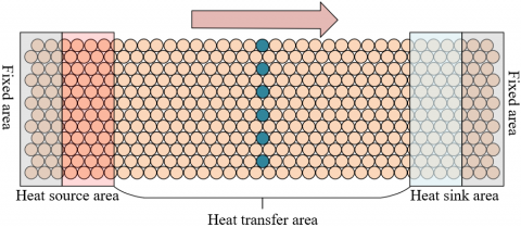
To optimize the positions of Si and Ge atoms in the nanowire structure, this paper chose to use the conjugate gradient method to minimize the total energy of the constructed model, and then simulated the equilibrium state of energy distribution in the 2ns simulation environment. At last, a temperature gradient was introduced into the equilibrium state simulation in the 4ns simulation environment. Figure 1 shows the heat transfer mechanism of nanowires.
Figure 1. The heat transfer mechanism of nanowires
Assuming: P represents the cross-sectional area of the nanowire; dW/dr represents the energy transfer rate in the constant temperature area, then the heat flux transferred from the heat source area to the heat sink area can be calculated by the following formula:
$VC=\frac{dW/dr}{P}$ (15)
Assuming: dR/dτ represents the temperature gradient along the direction of the heat flux, then the thermal conductivity after the model has stabilized can be calculated by the following formula:
$\eta =-\frac{VC}{dR/d\tau }$ (16)
The heat transfer in the nanowire structure of microelectronic equipment is greatly affected by the size of the cross-section of nanowires. Super lattice nanowires with larger cross-section sizes have lower thermal conductivity, namely their thermal conductivity coefficients are smaller. This paper introduced the phonon state density to verify the above conclusion, and this parameter can be regarded as a Fourier transform of the autocorrelation function of the Si and Ge atoms in the nanowire structure, and its expression is:
$GB\left( \theta \right)=\int_{-\infty }^{+\infty }{{{o}^{-\theta r}}UX\left( r \right)}dr$ (17)
Assuming: M represents the total number of Si and Ge atoms in the nanowire structure; u(r) represents the atom velocity vector at time moment t; u(0) represents the initial velocity of the atom; < > represents the averaging operation, then the autocorrelation of velocity UX(r) can be defined by the following formula:
$UX\left( r \right)=\frac{1}{M}\sum\limits_{i=1}^{M}{\left\langle {{u}_{i}}\left( 0 \right){{u}_{i}}\left( r \right) \right\rangle }$ (18)
For nanowire structures in microelectronic equipment with different shapes of cross section, there’re certain differences in the correlation dynamics, and such differences can lead to large differences in the same-type phononic crystals at the macro level and completely different elastic wave transmission behaviors.
A very important research purpose of this paper is to adjust the thermal conductivity of nanowires through the geometry of the cross-section of nanowires. For nanowires of a same cross-sectional area, if the shapes of their cross-sections are different, then there will be great differences in the ratio of surface area to volume, and their thermal conductivity will be different as well. Calculating the phonon participation rate which can quantitatively describe the localization effect of phonons is an effective way to research the phonon activity, and the phonon state density of the i-th nanowire structure Si and Ge atom with a frequency of θ is defined by the following formula:
$GS\left( \upsilon \right)=\frac{1}{M}\frac{{{\left( \sum\nolimits_{i}{G{{B}_{i}}{{\left( \upsilon \right)}^{2}}} \right)}^{2}}}{\sum\nolimits_{i}{G{{B}_{i}}{{\left( \upsilon \right)}^{4}}}}$ (19)
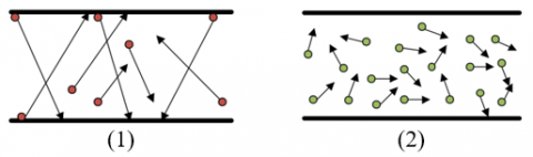
Figure 2. The phonon transmission effect under the conditions of different total sample lengths
For nanowires with a periodic length showing gradient distribution and nanowires with a periodic length showing non-gradient distribution, there’re differences in the degree of influence of the total sample length on the thermal conductivity. Figure 2 shows the phonon transmission effect under the conditions of different total sample lengths. When the total length of the sample is shorter, the phonons are under a ballistic transport state, as shown in Figure 2-1; when the total length of the sample is longer, the phonons are under a diffused transport state, as shown in Figure 2-2. Under certain extreme conditions, the effective thermal conductivity of nanowire super lattices in the microelectronic equipment is not affected by the total sample length. Assuming: for nanowires with a periodic length showing gradient distribution, the thermal conductivity of each component in a cycle is represented by H1 and H2; the thermal resistance of interface is represented by SZ; the periodic length is represented by KS, then the effective thermal conductivity coefficient of nanowire structure under extreme conditions can be calculated by the following formula:
$l=\frac{{{K}_{S}}{{H}_{1}}{{H}_{2}}}{{{H}_{1}}+{{H}_{2}}+2SZ{{H}_{1}}{{H}_{2}}}$ (20)
The Kapitza heat resistance which describes the thermal conductivity of the grain boundary can be calculated by the following formula:
$H=\frac{1}{SZ}=\frac{VC}{\Delta R}$ (21)
To attain the accurate value of thermal conductivity of ultra-long nanowires, assuming: all phonons are in the single mode, the relationship between thermal conductivity and total sample length is derived based on the Boltzmann transport equation and the Matthiessen’s rule; l represents the thermal conductivity at a given sample length of K; l∞ represents the thermal conductivity of ultra-long super lattice nanowires; kES represents the mean free path of effective phonons, then there is:
$\frac{1}{l}=\frac{1}{{{l}_{\infty }}}\left( \frac{{{k}_{ES}}}{K}+1 \right)$ (22)
By changing the total sample length in the simulation tests, a series of thermal conductivity values of nanowires with a periodic length showing gradient distribution can be obtained. Then, the curves of the obtained data were fitted based on the least square method, and the results suggested that there’s a significant linear correlation between 1/l and 1/K.
For nanowires with a periodic length showing different gradient distributions, the thermal conductivity fluctuated slightly with the rise of temperature, and it can be approximately considered to be unchanged. Phonon localization may be the reason for the unstable thermal conductivity of nanowires with non-uniformly distributed periodic length under the condition of temperature change. This paper chose to use the Kapitza heat resistance to describe the localization effect of phonons. Assuming: ΔR represents the temperature drop at the nanowire interface; VC represents the heat flux, then the Kapitza heat resistance can be calculated by the following formula:
$T=\frac{\Delta R}{VC}$ (23)
Based on the calculation results of thermal resistance of nanowire interface with different gradient distributions, it can be known that the mismatch of adjacent layers of nanowires will enhance the phonon localization effect, and ultimately increase the thermal resistance of the interface.
SiC material is a covalent bond compound that can hardly be found in nature, however, due to its excellent properties such as wide bandwidth, high strength and high thermal conductivity, the power devices fabricated based on the SiC material can serve as ideal substitutes for silicon power devices, and they have a very good prospect to be applied in miniature electronic equipment. Compared with the nano-scale Si/Ge material, the nano-scale SiC material has a larger surface volume ratio, so studying the heat transfer of the nano-scale SiC material is particularly important for improving the integration degree of power devices and increasing their functions.
In this study, the structure of the nano-scale SiC material was simulated. At first, an initial crystal cell model of the nanometer material was constructed. To ensure that the total number of atoms in the structure is fixed, this paper adopted the boundary conditions of nanowires with a periodic length showing gradient distribution to control the size of the cut-off radius. A properly-selected cut-off radius can ensure that the computer can simulate the nanostructure model faster and more accurately. In addition, to ensure that the simulation process of the nanostructure model is meaningful and the simulation results are close to the actual situation, this paper optimized the structure of the nanostructure model optimized based on the Discover Minimization module.
To make the nanostructure model reach the equilibrium state at an ideal velocity, the queues and the initial velocity of atoms in the model must be the same with those in the actual situation, so this paper adopted the Maxwell distribution to judge whether the atom velocity and distribution have both reached the initial equilibrium. Assuming: n represents the atom mass; χ represents the system temperature; u represents the direction velocity; LY represents the Boltzmann constant, then the expression of the Maxwell distribution is:
$g\left( u \right)=4\pi {{u}^{2}}{{\left( \frac{n}{2\pi {{L}_{Y}}\chi } \right)}^{3/2}}exp\left( -\frac{n{{u}^{2}}}{2{{L}_{Y}}\chi } \right)$ (24)
After normalization, there is:
$\int_{-\infty }^{\infty }{g\left( u \right)}du=1$ (25)
Assuming: SH represents the volume specific heat of the structure of the nano-scale SiC material; u represents the average velocity of the phonons; kVB represents the mean free path of the effective phonons of the material, then, based on the gas dynamics, the thermal conductivity of medium can be calculated by the following formula:
$l=\frac{1}{3}SHu{{k}_{eVB}}$ (26)
Similarly, the thermal conductivity of the structure of the nano-scale SiC material is constrained by the size of the sample. If the sample amount is far greater than kVB, then the constrain of size could be ignored. Assuming: K represents the length of the simulation domain of the sample; k∞ represents the mean free path of an infinite system, then there is:
$\frac{1}{{{k}_{VBf}}}=\frac{1}{{{k}_{\infty }}}+\frac{1}{K}$ (27)
According to the above formula, we can get the same conclusion of Formula 22, that there’s a significant linear correlation between 1/l and 1/K. The convergent thermal conductivity of the sample volume of the nano-scale SiC material can be attained by extrapolating the size of the simulation domain to 1/K= 0.
In the experiment, at first, for the structure of Si/Ge nanowires in the microelectronic equipment, the relationship between thermal conductivity and periodic length was studied. The total length of the sample was about 36 nm, and the variation range of the periodic length of the nanowire structure was [0.5nm, 28.6nm]. Figure 3 shows the relationship between thermal conductivity and periodic length. As can be seen in the figure, with the increase of periodic length, the heat transfer performance of the uniform-cycle Si/Ge nanowire structure lattices showed an obvious non-monotonous trend.
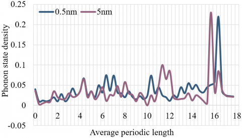
To figure out the mechanism of phonon transmission in uniform-cycle Si/Ge nanowire structure lattices, this paper calculated the phonon state density of nanowire structure lattices under the conditions of different periodic lengths, and the statistical results are given in Figure 4. As can be seen in the figure, with the increase of periodic length, the number of significant peaks of the phonon state density decreased, indicating that the coherent phonons formed on the crystal lattices of the Si/Ge nanowire structure would decrease sharply with the increase of periodic length, which is consistent with the analysis result of Figure 3.
Figure 3. Relationship between thermal conductivity and periodic length
Figure 4. Relationship between phonon state density and average periodic length
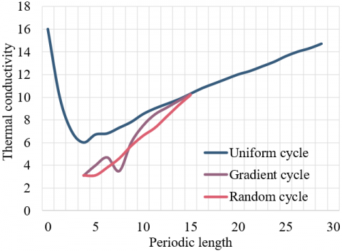
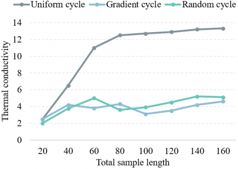
Figure 5. Relationship between thermal conductivity and total sample length
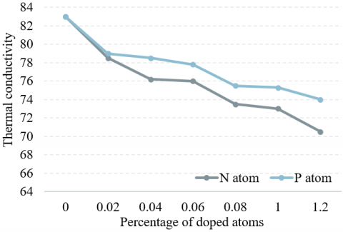
Table 2. The change of thermal conductivity of the nano-scale SiC material with the percentage of doped atoms
|
Percentage of doped atoms |
Thermal conductivity in case of N atom substitution |
Thermal conductivity in case of P atom substitution |
|
0.041287 |
83.412 |
88.429 |
|
0.062359 |
78.529 |
72.617 |
|
0.074815 |
75.416 |
70.529 |
|
0.081251 |
70.632 |
77.596 |
|
0.095826 |
77.584 |
71.518 |
|
0.072151 |
71.629 |
75.916 |
|
0.136258 |
79.538 |
73.591 |
Figure 6. The change of thermal conductivity of the nano-SiC material with the percentage of doped atoms
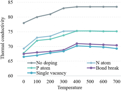
Figure 7. The change of thermal conductivity of the nano-SiC material under different doping conditions with the temperature
Figure 5 shows the relationship between thermal conductivity and total sample length of the Si/Ge nanowire structure with uniform cycle, gradient cycle, and random cycle. The periodic length corresponding to the minimum thermal conductivity of the nanowire structure lattices was 3.95nm. According to the figure, for uniform-cycle Si/Ge nanowire structure lattices, with the increase of total sample length, the thermal conductivity increased first and then tended to be saturated. The main reason is that the total sample length was less than the mean free path of effective phonons, phonons with longer wavelengths cannot perform effective scattering, they coherently passed through the shorter nanowire structure lattices, which led to an increase in the thermal conductivity coefficient.
The physical and chemical properties of the nano-scale SiC material will change greatly due to factors such as doping and vacancy. This paper also studied the relationship between the thermal conductivity of the nano-scale SiC material and the percentage of doped atoms. Table 2 gives the thermal conductivity of the nano-scale SiC material with a percentage of doped atoms of 0.041287%, 0.062359%, 0.074815%, 0.081251%, 0.095826%, 0.072151%, and 0.136258%, respectively. Figure 6 gives the change of the thermal conductivity of the nano-SiC material with the percentage of doped atoms in case of N atom substitution and P atom substitution. As can be seen from the figure, with the increase of N atom substitution, the thermal conductivity of the nano-SiC material showed a decline trend; and in case of P atom substitution, such decline trend was more obvious. The main reason is that, the greater the percentage and mass of doped atoms, the smaller the thermal conductivity of the material, and the less obvious the changes in the thermo-physical properties.
Figure 7 gives the change of thermal conductivity of the nano-SiC material under different doping conditions with the temperature. According to the figure, the thermal conductivity of the nano-SiC material without doping was the largest, and the thermal conductivity of the nano-SiC material with single vacancy was the smallest. Although the thermal conductivity of the nano-SiC material in case of N atom substitution was greater than that of the nano-SiC material in case of P atom substitution, the difference was not much. Referring to the existing research conclusions, it can be considered that compared with doped nano-SiC material, for nano-SiC materials with single vacancy or broken single bond under high-temperature conditions, the phonon scattering effect would be more obvious. While for nano-SiC materials with single vacancy or broken single bond under low-temperature conditions, it’s hard to excite more high-energy quantum.
This paper studied the thermo-physical properties of nanostructure in microelectronic equipment. At first, by structuring Si super lattice nanowires in a specific direction and then using the Ge atoms to replace the Si atoms in nanowires, this paper built a model for the periodic Si/Ge super lattice nanowires. Then, this paper performed integral operation on the dynamic equations of the two types of atoms using the time integration algorithm to attain the trajectories of Si and Ge atoms in the nanowire structure of microelectronic equipment, and discussed the influence of the size and geometrical shape of the cross section of nanowires on thermal conductivity. After that, this paper simulated the structure of the nano-scale SiC material, selected appropriate cut-off radius, and optimized the structure of the nanostructure model based on the Discover Minimization module.
Combining with experiment, this paper studied the relationship between the thermal conductivity of the Si/Ge nanowire structure in the microelectronic equipment and periodic length, calculated the phonon state density of nanowire structure lattices under the conditions of different periodic lengths, and gave the statistical results. After that, this paper compared the curves of the relationship between thermal conductivity and total sample length of the Si/Ge nanowire structure with uniform cycle, gradient cycle, and random cycle, and it can be known that for uniform-cycle Si/Ge nanowire structure lattices, with the increase of total sample length, the thermal conductivity increased first and then tended to be saturated. Moreover, this paper also studied the relationship between the thermal conductivity of the nano-scale SiC material and the percentage of doped atoms, plotted the change of thermal conductivity of the nano-SiC material under different doping conditions with the temperature, and analyzed the corresponding experimental results.
This paper was supported by the Key Laboratory of Special Material Connection and Energy Equipment Repair Technology (Grant No.: 2015JH-28).
[1] Bhardwaj, R., Chae, K.H., Goyal, N. (2020). Electronic structural study of defect-induced magnetism in Co doped ZnO nanostructure. Vacuum, 178: 109446. https://doi.org/10.1016/j.vacuum.2020.109446
[2] Dibble, J.P., Troyano-Valls, C., Tovar, J.D. (2020). A tale of three hydrophobicities: impact of constitutional isomerism on nanostructure evolution and electronic communication in π-conjugated peptides. Macromolecules, 53(17): 7263-7273. https://doi.org/10.1021/acs.macromol.0c01492
[3] Timoshnev, S.N., Benemanskaya, G.V., Kukushkin, S.A. (2020). Drastic change in surface electronic properties and creation of a new carbon-based nanostructure on the vicinal SiC (111)-4° surface. Journal of Physics: Conference Series, 1697(1): 012247. https://doi.org/10.1088/1742-6596/1697/1/012247
[4] Benchtaber, N., Nafidi, A., Barkissy, D., Boutramine, A., Benaadad, M., Melkoud, S., Es-Salhi, E.S. (2020). Theoretical electronic band structures and transport in InAs/GaSb type II nanostructure superlattice for medium infrared detection. Materials Today: Proceedings, 22: 41-44. https://doi.org/10.1016/j.matpr.2019.08.069
[5] Chuan, M.W., Wong, K.L., Hamzah, A., Rusli, S., Alias, N.E., Lim, C.S., Tan, M.L.P. (2020). Electronic properties and carrier transport properties of low-dimensional aluminium doped silicene nanostructure. Physica E: Low-dimensional Systems and Nanostructures, 116: 113731. https://doi.org/10.1016/j.physe.2019.113731
[6] Tao, D.W., Chen, J.B., Jiang, Z.J., Qi, B.J., Zhang, K., Wang, C.W. (2020). Making reversible transformation from electronic to ionic resistive switching possible by applied electric field in an asymmetrical Al/TiO2/FTO nanostructure. Applied Surface Science, 502: 144124. https://doi.org/10.1016/j.apsusc.2019.144124
[7] Khakhomov, S.A., Semchenko, A.V., Sidsky, V.V., et al. (2017). Nanostructure and ferroelectric properties of sol-gel SBTN-films for electronic devices. In International Conference on Global Research and Education, Iași, Romania, pp. 144-150. https://doi.org/10.1007/978-3-319-67459-9_19
[8] Gündüz, B., Kurban, M. (2018). Photonic, spectroscopic properties and electronic structure of PTCDI-C8 organic nanostructure. Vibrational Spectroscopy, 96: 46-51. https://doi.org/10.1016/j.vibspec.2018.02.008
[9] Wang, Y., Sheng, X., Yuan, Q., et al. (2018). Carrier dynamics in hybrid nanostructure with electronic coupling from an InGaAs quantum well to InAs quantum dots. Journal of Luminescence, 202: 20-26. https://doi.org/10.1016/j.jlumin.2018.05.029
[10] Miao, P., Wang, J., Zhang, C., Sun, M., Cheng, S., Liu, H. (2019). Graphene nanostructure-based tactile sensors for electronic skin applications. Nano-Micro Letters, 11(1): 71. https://doi.org/10.1007/s40820-019-0302-0
[11] Alborznia, H., Naseri, M., Fatahi, N. (2019). Buckling strain effects on electronic and optical aspects of penta-graphene nanostructure. Superlattices and Microstructures, 133: 106217. https://doi.org/10.1016/j.spmi.2019.106217
[12] Gensch, M., Schwartzkopf, M., Ohm, W., et al. (2019). Correlating nanostructure, optical and electronic properties of nanogranular silver layers during polymer-template-assisted sputter deposition. ACS Applied Materials & Interfaces, 11(32): 29416-29426. https://doi.org/10.1021/acsami.9b08594
[13] Amodio, A., Del Grosso, E., Troina, A., Placidi, E., Ricci, F. (2018). Remote electronic control of DNA-based reactions and nanostructure assembly. Nano Letters, 18(5): 2918-2923. https://doi.org/10.1021/acs.nanolett.8b00179
[14] Neshani, S., Ahmadi, M.T., Rahmani, M. (2022). Theoretical analysis on the electronic properties of bubble-wrap carbon nanostructure: fullerene-doped graphene. Journal of Computational Electronics, 21(1): 214-226. https://doi.org/10.1007/s10825-021-01826-0
[15] Balamurugan, C., Cho, K., Park, B., et al. (2022). Large modulation of the chemical and electronic sensitization of TiO2/Ag/NiO nanostructure via in situ hydrothermal-induced heterointerface engineering. Chemical Engineering Journal, 430: 132690. https://doi.org/10.1016/j.cej.2021.132690
[16] Alborznia, H., Amirian, S., Nazirzadeh, M. (2022). Buckling variation effects on optical and electronic properties of GeP2S nanostructure: A first-principles calculation. Optical and Quantum Electronics, 54(10): 608. https://doi.org/10.1007/s11082-022-04055-2
[17] Wang, X., Liu, B., Xiao, X., Wang, S., Huang, W. (2021). Boron dopant simultaneously achieving nanostructure control and electronic structure tuning of graphitic carbon nitride with enhanced photocatalytic activity. Journal of Materials Chemistry C, 9(41): 14876-14884. https://doi.org/10.1039/D1TC04142H
[18] Jia, Q., Mu, Z., Zhang, X., et al. (2021). Electronic conductive and corrosion mechanisms of dual nanostructure CuCr-doped hydrogenated carbon films for SS316L bipolar plates. Materials Today Chemistry, 21: 100521. https://doi.org/10.1016/j.mtchem.2021.100521
[19] Yue, O., Wang, X., Liu, X., Hou, M., Zheng, M., Wang, Y., Cui, B. (2021). Spider-web and ant-tentacle doubly bio‐inspired multifunctional self-powered electronic skin with hierarchical nanostructure. Advanced Science, 8(15): 2004377. https://doi.org/10.1002/advs.202004377
[20] Zhuang, X., Zhou, Y., Jiang, Z., Yao, X., Yu, X.Y. (2021). Synergetic electronic modulation and nanostructure engineering of heterostructured RuO2/Co3O4 as advanced bifunctional electrocatalyst for zinc-air batteries. Journal of Materials Chemistry A, 9(47): 26669-26675. https://doi.org/10.1039/D1TA09278B
[21] Jian, K., Ma, W., Lv, Z., Wang, M., Lv, X., Li, Q., Dang, J. (2021). Tuning the electronic structure of the CoP/Ni2P nanostructure by nitrogen doping for an efficient hydrogen evolution reaction in alkaline media. Inorganic Chemistry, 60(23): 18544-18552. https://doi.org/10.1021/acs.inorgchem.1c03145
[22] Saleem, A., Zhang, Y., Gong, H., et al. (2020). Carbon nanostructure-reinforced SiCw/Si3N4 composite with enhanced thermal conductivity and mechanical properties. RSC Advances, 10(25): 15023-15029. https://doi.org/10.1039/D0RA00876A
[23] Nakamura, Y. (2018). Nanostructure design for drastic reduction of thermal conductivity while preserving high electrical conductivity. Science and Technology of advanced MaTerialS, 19(1): 31-43. https://doi.org/10.1080/14686996.2017.1413918
[24] Juraev, H.S., Juraeva, G.H. (2022). Investigation of thermal conductivity of nanostructures using a mathematical model. Journal of Physics: Conference Series, 2270(1): 012015. https://doi.org/10.1088/1742-6596/2270/1/012015