Bahareh Safari | Seyed Ebrahim Hosseini*
© 2021 IIETA. This article is published by IIETA and is licensed under the CC BY 4.0 license (http://creativecommons.org/licenses/by/4.0/).
OPEN ACCESS
The combination of two techniques: low-bandgap semiconductor and line-tunneling structure is an effective way to achieve the highest on-current in TFETs. In this paper, design of low-bandgap line-tunneling TEFT and its analytical modeling of drain current equation is proposed. The previously suggested drain current equation for the low-bandgap line-tunneling TEFT has been explained in a relatively complex form based on the minimum tunnel path that is an effective factor in determining band-to-band tunneling (BTBT). It has been simplified in this paper and reformulated based on gate-to-source voltage. Important design factors such as source doping concentration, material and thickness of the gate-insulator were examined by simulation and numerical calculations based on the minimum tunnel path for two low-bandgap In0.88Ga0.12As and relatively high-bandgap GaSb semiconductors. The comparison of the results obtained from simulations with the proposed analytical drain current model show a good agreement. Drain doping concentration, is an effective factor on the off-state current of low-bandgap TFET. This factor was examined in order to reduce the off-current.
analytical modelling, line-tunneling, low-bandgap semiconductor, minimum tunnel path, tunnel field-effect transistor (TFET)
Nowadays, the down-scaling of conventional MOSFET has led to increase in power consumption [1-4] that has been called as the power crisis [1, 3]. The mechanism of MOSFET transistors operation does not allow subthreshold swing less than 60 mV/dec [5-7]. Tunnel field-effect transistor (TFET) is defined as a semiconductor device in which the gate controls the source-drain current through modulation of Band-to-Band Tunneling (BTBT) and Band-to-Band Tunneling is a process in which electrons tunnel from the valence band through the semiconductor bandgap to the conduction band [8]. The TFET is suitable for low power consumption applications because of its low subthreshold swing and low off-state leakage current. [9-13]. However, Si-based TFETs have a low on-current due to their high-bandgap [14-16]. It has been proved that using low-bandgap semiconductors increases the on-current (Ion) of TFET [17-20] although the low-bandgap in these semiconductors, reduces the undesirable tunnel length at the channel-drain side and increases significantly the off-current (Ioff) [16]. Reducing the drain doping concentration has an important role in decreasing the tunneling of the drain side and controlling the off-current [16]. In the low-bandgap TFET the effect of drain-source voltage (Vds) controlling is more due to its low-bandgap. When (Vds) goes beyond the bandgap voltage (Eg/q), the undesirable tunnel length is significantly decreased. Using gate-source overlap structure or line-tunneling structure is another effective way to increase the on-current in TFETs [1, 8, 21]. Combining the line-tunneling structure and the low-bandgap semiconductor is an effective way to achieve the highest on-current in TEFT [22]. The tunnel path is defined as the physical path between two points corresponding to equal energy for the conduction and valence band respectively [8]. Since the minimum tunnel path (lmin) which is the minimum length of tunnel path in the depletion region, has a great effect in determining the amount of the line-tunneling TFET current, important parameters of design such as: source doping concentration, material and the thickness of gate-insulator were investigated by simulation and numerical calculations based on the minimum tunnel path (lmin) for two semiconductors, low-bandgap In0.88Ga0.12As and relatively high-bandgap GaSb. The previously proposed current equation for low-bandgap line-tunneling TEFT [22] based on lmin is relatively complex. It has been simplified in this paper and it has also been reformulated based on the gate-to-source voltage (Vgs). Then, a comparison has been made between the results obtained from the proposed model and the results obtained from the previous model [22] and the simulation results for several different source doping concentrations, gate-insulator with different materials and thicknesses, which showed a good agreement.
2.1 Structure and parameters
Figure 1 shows a schematic sketch of the line- and point-tunneling TEFTs used in this study. Direct bandgap of 0.5 eV In0.88Ga0.12As with work function of 4.7 eV is considered as the low-bandgap semiconductor and direct bandgap of 0.72 eV GaSb with the work function of 4.12 eV is considered as the relatively high-bandgap semiconductor. Table 1 shows the parameters of TFETs used in investigation.
The simulations were done using the Silvaco software package and using non-local tunneling.
Figure 1. Schematic structures of (a) line-tunneling and (b) point- tunneling, TFETs
Table 1. Parameters of TFETs
|
Gate-source overlap length |
80 nm |
|
Channel length |
50 nm |
|
Body thickness |
40 nm |
|
Source doping concentration |
8×1018 cm-3 |
|
Drain doping concentration |
1018 cm-3 |
|
Channel doping concentration |
1016 cm-3 |
|
Gate insulator material |
HfO2 |
|
Gate insulator thickness |
1 nm |
2.2 Analytical model
The analytical model used in this paper is line-tunneling TFET analytical model presented in ref. [22] in which the minimum tunnel path is calculated as an indicator of line-tunneling TFETs. In this model minimum tunnel path (lmin) and maximum tunnel path (lmax), are expressed in Eq. (1) and Eq. (2) as follows
${{l}_{\max }}=\sqrt{2\varepsilon {{E}_{g}}/{{q}^{2}}{{N}_{a}}}$ (1)
where, ε is the dielectric permittivity of the semiconductor, Eg is the bandgap energy of the semiconductor, Na is the source doping concentration and q is the electron charge.
${{l}_{\min }}={{l}_{\max }}.(\sqrt{q{{\psi }_{s}}/{{E}_{g}}}-\sqrt{q{{\psi }_{s}}/{{E}_{g}}-1})$ (2)
where, ψs is the surface potential at the semiconductor-insulator interface. For small body-effect coefficient (γ), can be written as follows
${{\psi }_{s}}={{V}_{gs}}-{{V}_{fb}}-\gamma \sqrt{{{V}_{gs}}-{{V}_{fb}}}$ (3)
where, Vfb is the flat-band voltage. The drain current of the low-bandgap line-tunneling TEFT is written based on lmin parameter as follows
$I=(Aq{{N}_{a}}E_{g}^{1/2}{{l}_{\max }}/12\varepsilon ).{{({{l}_{\max }}/{{l}_{\min }})}^{3}}.\exp (-BqE_{g}^{1/2}{{L}_{\min }})$ (4)
In this paper, the coefficients $A=q^{2} \sqrt{m_{r}} / 18 \pi \hbar^{2}$ and $B=\pi \sqrt{m_{r}} / 2 \hbar q$ in Eq. (4), for line-tunneling TFET based on In0.88Ga0.12As semiconductor are 2.64 × 10²⁰ eV1/2.V-2.cm-1.s-1 and 15.44×10⁶ V.cm-1.eV-3/2, respectively. Here mr and ћ are the reduced mass and the reduced Plank’s constant respectively.
2.3 Operation investigation
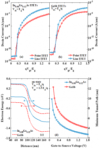
The lateral tunneling or point-tunneling occurs in parallel with the semiconductor-gate insulator surface while vertical tunneling happens perpendicular with the semiconductor-gate-insulator surface in the gate-source overlap. Vertical tunneling is also called line-tunneling since the vertical tunneling area is similar to a line which becomes important in higher Vgs [23]. Figures 2(a) and 2(b) show the simulated Ids-Vgs characteristics of line- and point-tunneling TFETs for In0.88Ga0.12As and GaSb. It can be seen that the line-tunneling TEFT in both semiconductors has a higher on-current and smaller subthreshold swing than the point-tunneling TFET. To be exact, point subthreshold swings are 8.5 mV/dec and 15.84 mV/dec for In0.88Ga0.12As line- and point-tunneling TFETs respectively, and 11.84 mV/dec and 32.75 mV/dec for GaSb line- and point-tunneling TFETs respectively.
Figure 2. Ids–Vgs characteristics for point- and line-tunneling TFETs using (a) In0.88Ga0.12As, and (b) GaSb. (c) on-state energy-bands diagram of In0.88Ga0.12As and GaSb line-tunneling TFETs. (d) Calculated on-state minimum tunnel path as function of gate voltage for In0.88Ga0.12As and Gasb line-tunneling TFETs
In the line-tunneling TFET, as Vgs is increasing, charge inversion is formed beneath the gate in the source region and electrons tunnel from the source to the newly inverted source region. When Vgs is close to the threshold voltage, this tunneling increases and decreases the subthreshold swing of line-tunneling TFET. Furthermore, in the line-tunneling TFET, both line-tunneling and point-tunneling are done and there are more electrons in the channel; therefore, on-current of the line-tunneling TFET becomes higher than point-tunneling TFET. Figure 2(a) and 2(b) also show that the line-tunneling TEFT based on In0.88Ga0.12As low-bandgap semiconductor has higher on-current and smaller subthreshold swing than the line-tunneling TFET based on GaSb high-bandgap semiconductor. Figure 2(c) shows the on-state energy-bands diagram of the In0.88Ga0.12As and GaSb TEFTs. As it is seen in these energy-bands diagram, the In0.88Ga0.12As TEFT has a smaller tunnel length than the GaSb high-bandgap TEFT. The smaller tunnel length results in more BTBT generation and consequently increase in the on-current.
Figure 3. Ids–Vgs characteristics for line-tunneling TEFTs using (a) In0.88Ga0.12As and (b) GaSb, for various drain-source voltages. (c) off-state energy-bands diagram of In0.88Ga0.12As line-tunneling TFETs for various drain-source voltages. (d) on-state energy-bands diagram of In0.88Ga0.12As line-tunneling TFETs for various gate-source voltages
Figure 2(d) shows the calculation of lmin as function of Vgs for two semiconductors In0.88Ga0.12As and GaSb. As it is observed, lmin is strongly dependent on Eg. The In0.88Ga0.12As line-tunneling TEFT, has smaller lmin than GaSb. This issue causes sooner initiation of line-tunneling that results in the improvement of subthreshold swing and higher on-current of the In0.88Ga0.12As line-tunneling TEFT compared with GaSb line-tunneling TEFT. Figures 3(a) and 3(b) show the dependence of the Ids–Vgs characteristic of the simulated line-tunneling TEFTs for different values of Vds for two semiconductors. As Vds goes higher than bandgap voltage (Eg/q), undesirable tunneling at channel-drain side increases because the tunnel length at the channel-drain side becomes thinner and it also increases off-current and subthreshold swing while, the increase of on-current is negligible. Figure 4(c) shows off-state energy-bands diagram for In0.88Ga0.12As TFET for different values of Vds. In this figure, the narrowing of channel-drain side tunnel length is well seen. Moreover, increase in Vds also increases the diode leakage current and helps increase the off-current. In order to avoid increase in the off-current and also improve the subthreshold swing, Vds for both semiconductors is assumed to be equal to the bandgap voltage (Eg/q) of that semiconductor. Figure 2(d) shows that the variations of lmin with Vgs are exponential for both semiconductors and this shows the extreme dependence of lmin to Vgs. The decrease in lmin with increase in Vgs leads to increase in the on-current and improvement of the subthreshold swing. However, lmin is saturated and on-current almost remains stable for high Vgs. Figure 3(d) shows the on-state energy-bands diagram of In0.88Ga0.12As line-tunneling TEFT for different values of Vgs. Increase in Vgs results in a reduction of the tunnel length and it causes an increase in BTBT generation and consequently an increase in the on-current and improvement in the subthreshold swing. However, lowering of tunnel length is saturated and on-current almost remains constant for high Vgs. The value of Vgs was considered to be 1.5 times that of the bandgap voltage (Eg/q) of that semiconductor in order to assure the high on-current and desirable subthreshold swing.
3.1 Source doping concentration
Figures 4(a) and 4(b) show the dependence of the line-tunneling TEFT current on the source doping concentration for two In0.88Ga0.12As and GaSb semiconductors. As the source concentration increases, the off-current decreases due to increased recombination of the carriers participating in the off-current; In addition, the on-current increases and the subthreshold swing decreases. However, it can be seen that for heavy doping concentrations, the subthreshold swing increases again. The increase in the source doping concentration decreases the point-tunneling onset voltage while it increases the line-tunneling onset voltage and also the on-current of line-tunneling [23]. For high source doping concentrations when Vgsbecomes near the threshold voltage, vertical tunneling is more effective in determining the subthreshold swing conditions. However, for heavy source doping concentrations, the line-tunneling onset voltage increases and lateral tunneling becomes dominant in determining the subthreshold swing conditions. Using a source with heavy doping concentration provides the considered on- and off-current; but increases the subthreshold swing. Figure 4(c) shows the on-state energy-bands diagram of In0.88Ga0.12As line-tunneling TFET. It can be seen that increasing the source doping concentration causes decrease of the tunnel length that results in an increase in the on-current. However, in heavy doping concentrations the decrease in the tunnel length is saturated and the tunneling generation and consequently the on-current stays approximately constant. Figure 4(d) shows the calculated lmin for different values of the source doping concentration for two semiconductors. With increase in the source doping concentration, lmin decreases and becomes saturated in heavy doping concentrations and the on-current stays approximately constant. Thus, the source doping concentration has been considered to 8×1018 cm-3 in order to improve the conditions of subthreshold swing.
Figure 4. Ids–Vgs characteristics for line-tunneling TEFTs using (a) In0.88Ga0.12As and (b) GaSb, with various source doping concentrations. (c) on-state energy-bands diagram of In0.88Ga0.12As line-tunneling TFETs for various source doping concentrations. (d) Calculated on-state minimum tunnel path against source doping concentration for In0.88Ga0.12As and GaSb line-tunneling TFETs
3.2 Gate-insulator material
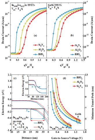
Figures 5(a) and 5(b) show the Ids-Vgs characteristics for three different gate-insulators of Si3N4, Al2O3 and HfO2, for two In0.88Ga0.12As and GaSb semiconductors. As it can be seen, the gate-insulator material does not affect the off-current but with increasing the dielectric constant, the on-current and the subthreshold swing improve. Figure 5(c) shows the on-state energy-bands diagram of the line-tunneling TEFT for two different gate-insulators of HfO2 and Si3N4. Using the gate-insulator with the higher dielectric constant causes a more powerful capacitor and more bending of energy-bands; thus tunneling begins at a lower voltage and the on-current increases and the subthreshold swing decreases. Calculating the minimum tunnel path in Figure 5(d) shows that using the gate-insulator with higher dielectric constant decreases the lmin in lower Vgs and causes the tunneling to begin in a lower voltage. The smaller lmin at higher dielectric constants justifies the higher on-current and the lower subthreshold swing of TEFTs.
Figure 5. Ids–Vgs characteristics for line-tunneling TFETs using (a) In0.88Ga0.12As, and (b) GaSb, for different gate-insulators. (c) on-state energy-bands diagram of In0.88Ga0.12As line-tunneling TFETs for two different gate-insulators. (d) Calculated on-state minimum tunnel path as function of gate voltage for In0.88Ga0.12As and GaSb line-tunneling TFETs for different gate-insulators
3.3 Gate-insulator thickness
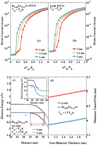
Changing the thickness of the gate-insulator does not have much effect on the off-current. However, as it is seen in Figure 6(a) and 6(b) that using a thinner gate-insulator has improved the on-current and the subthreshold swing. Figure 6(c) shows the on-state energy-bands diagram of the In0.88Ga0.12As line-tunneling TEFT for two different gate-insulator thicknesses. For a thin gate-insulator thickness, the bending of the energy-bands has increased because of the higher gate capacitor. Also, lmin increases linearly with the increase in gate-insulator thickness in the calculations done as shown in Figure 6(d). However, the reduction of the gate-insulator thickness is a weak function in reducing the minimum tunnel path; while a thin gate-insulator initiates tunneling at a small Vgs and improves the on-current and the subthreshold swing.
Figure 6. Ids–Vgs characteristics for line-tunneling TFETs using (a) In0.88Ga0.12As, and (b) GaSb, for various Gate-insulator thicknesses. (c) on-state energy-bands diagram of In0.88Ga0.12As line-tunneling TFETs for various Gate-insulator thicknesses. (d) Calculated on-state minimum tunnel path against Gate-insulator thickness for In0.88Ga0.12As and GaSb line-tunneling TFETs
Since low-bandgap line-tunneling TFET current of Eq. (4) is complicated, in this section we simplify the current equation for In0.88Ga0.12As low-bandgap semiconductor by appropriate approximations, without losing accuracy. By inserting Eq. (2) in the pre-exponential term (lmax/lmin)3 of Eq. (4) we have the following:
${{({{l}_{\max }}/{{l}_{\min }})}^{3}}={{[1/(\sqrt{q{{\psi }_{s}}/{{E}_{g}}}-\sqrt{q{{\psi }_{s}}/{{E}_{g}}-1})]}^{3}}$ (5)
If we multiply $1 /\left(\sqrt{q \psi_{s} / E_{g}}-\sqrt{q \psi_{s} / E_{g}-1}\right)$ in Eq. (5) by $\left(\sqrt{q \psi_{s} / E_{g}}+\sqrt{q \psi_{s} / E_{g}-1}\right) /\left(\sqrt{q \psi_{s} / E_{g}}+\sqrt{q \psi_{s} / E_{g}-1}\right)$, after approximation and simplification we have the following:
${{({{l}_{\max }}/{{l}_{\min }})}^{3}}\cong {{(2q{{\psi }_{s}}/{{E}_{g}}+1/9)}^{2}}-4.16$ (6)
On the other hand, by inserting Eq. (2) in the exponential term in Eq. (4) and multiplying exponential argument by: $\left(\sqrt{q \psi_{s} / E_{g}}+\sqrt{q \psi_{s} / E_{g}-1}\right) /\left(\sqrt{q \psi_{s} / E_{g}}+\sqrt{q \psi_{s} / E_{g}-1}\right)$, we have,
$\exp (-BqE_{g}^{1/2}{{l}_{\min }})=\exp [-BqE_{g}^{1/2}{{l}_{\max }}\sqrt{{{E}_{g}}/q}/(\sqrt{{{\psi }_{s}}}+\sqrt{{{\psi }_{s}}-{{E}_{g}}/q})]$ (7)
Since the fraction term in Eq. (7) is rather complicated, it can be approximated as:
$\exp (-BqE_{g}^{1/2}{{l}_{\min }})\cong \exp (-B{{q}^{1/2}}{{E}_{g}}{{l}_{\max }}/2\sqrt{{{\psi }_{s}}-{{E}_{g}}/2q})$ (8)
If $k_{1}=A q N_{a} E_{g}^{1 / 2} l_{\max } / 12 \varepsilon$ and $k_{2}=B q^{1 / 2} E_{g} l_{\max } / 2$ by inserting Eq. (6) and Eq. (8) in Eq. (4), we have,
$\begin{aligned} I \cong & k_{1}\left[\left(2 q \psi_{s} / E_{g}+1 / 9\right)^{2}-4.16\right] \\ & . \exp \left(-k_{2} / \sqrt{\psi_{s}-E_{g} / 2 q}\right) \end{aligned}$ (9)
By inserting Eq. (3) in Eq. (9), we have,
$\begin{aligned} I \cong & k_{1}\left[\left(2 q\left(V_{g s}-V_{f b}-\gamma \sqrt{V_{g s}-V_{f b}}\right) / E_{g}+1 / 9\right)^{2}-4.16\right] \\ & \left.. \exp \left[-k_{2} /\left(V_{g s}-V_{f b}-\gamma \sqrt{V_{g s}-V_{f b}}\right)-E_{g} / 2 q\right)^{1 / 2}\right] \end{aligned}$ (10)
Figure 7. The Ids–Vgs characteristics for In0.88Ga0.12As line-tunneling TEFTs of equation (4), and (10) and results of simulation for (a) the main parameters of the paper, (b) three different values of source concentration, (c) three different gate-insulators, and (d) three different thicknesses of gate-insulators
In Figure 7 that shows a comparison between the drain current from Eq. (4) and the drain current from simplified Eq. (10) and the results of drain current obtained from the simulation for various different source doping concentrations and the gate-insulators with different materials and thicknesses indicates a good agreement. This indicates that the approximations made are correct.
5.1 Drain doping concentration
Figure 8. Ids–Vgs characteristics for line-tunneling TEFTs using (a) In0.88Ga0.12As and (b) GaSb, for various drain doping concentrations. (c) off-state energy-bands diagram of In0.88Ga0.12As and GaSb line-tunneling TFETs. (d) off-state energy-bands diagram of In0.88Ga0.12As TFETs for various drain concentrations
The drain doping concentration does not have any effect on the TEFT’s on-current. Controlling the drain doping concentration plays an important role in controlling the off-current in TEFTs [16]. Figures 8(a) and 8(b) show the Ids–Vgs characteristics of the line-tunneling TEFTs for different values of drain doping concentration for two semiconductors. It can be seen that with increase in the drain doping concentration, the off-current of line-tunneling TEFT and its subthreshold swing have increased while the on-current is fixed. The TEFT energy-bands diagram in the off-state have been drawn for two In0.88Ga0.12As and GaSb semiconductors in Figure 8(c). It can be seen that in the In0.88Ga0.12As line tunneling TEFT, the tunnel length of the channel-drain side is smaller; that results in the undesirable tunneling of the channel-drain side being more and this issue justifies its higher off-current. Figure 8(d) shows the TEFT energy-bands diagram of In0.88Ga0.12As in the off-state for different amounts of drain concentration. For high doping concentrations, the tunnel length of the channel-drain side decreases that results in an increase in the undesirable tunneling of electrons from the drain side and increases the off-current considerably. Increase in the off-current also increases the subthreshold swing. Using the drain with lower doping concentration decreases the off-current and improves the subthreshold swing. Although we must consider that in very low doping concentrations, a good ohmic connection is not established well on the drain side [3].
It was shown that using the low-bandgap line-tunneling TFET increases the on-current and improves the subthreshold swing. Important design factors such as source doping concentration, the material and thickness of the gate-insulator were considered by simulation and numeral calculations based on the minimum tunnel path. The factor that affects the off-current of the line-tunneling TFET is the drain doping concentration and its effect on the off-current was specified. The drain current equation of low-bandgap line-tunneling TFET was reformulated in a simpler form based on the gate-source voltage and it was shown that simplified equation is an agreement with the proposed drain current equation and simulation results.
|
A |
Parameter of Kane’s model, eV1/2.V-2.cm-1.s-1 |
|
B |
Parameter of Kane’s model, V.cm-1.eV-3/2 |
|
Eg ћ Ioff |
Bandgap energy of the semiconductor, eV Reduced Plank’s constant, eV.s Off current of TFET, A/µm or A |
|
Ion lmax lmin mr Na Np q Vds Vfb Vgs |
On current of TFET, A/µm or A Maximum tunnel path, m Minimum tunnel path, m Reduced mass, Kg Source doping concentration, cm-3 Drain doping concentration, cm-3 Electron charge, C Drain-to-source voltage, V Flat-band voltage, V Gate-to-source voltage, V |
|
Greek symbols |
|
|
$\gamma$ |
Body-effect coefficient, $\sqrt{V}$ |
|
$\varepsilon$ |
Dielectric permittivity of materials |
|
ψs |
surface potential at the semiconductor-insulator interface, V |
[1] Hu, C. (2008). Green transistor as a solution to the IC power crisis. Proceeding of 9th IEEE International Conference on Solid-State and Integrated-Circuit Technology, Beijing, pp. 16-20. https://doi.org/10.1109/ICSICT.2008.4735116
[2] Ionescu, A.M., Riel, H. (2011). Tunnel field-effect transistors as energy-efficient electronic switches. Nature, 479(7373): 329-337. https://doi.org/10.1038/nature10679
[3] Boucart, K. (2010). Simulation of double-gate silicon tunnel FETs with a high-k gate dielectric (No. THESIS). EPFL. https://doi.org/10.5075/epfl-thesis-4729
[4] Zhao, H., Chen, Y., Wang, Y., Zhou, F., Xue, F., Lee, J. (2011). InGaAs tunneling field-effect-transistors with atomic-layer-deposited gate oxides. IEEE Transactions on Electron Devices, 58(9): 2990-2995. https://doi.org/10.1109/TED.2011.2159385
[5] Choi, W.Y., Park, B.G., Lee, J.D., Liu, T.J.K. (2007). Tunneling field-effect transistors (TFETs) with subthreshold swing (SS) less than 60 mV/dec. IEEE Electron Device Letters, 28(8): 743-745. https://doi.org/10.1109/LED.2007.901273
[6] Koester, S., Lauer, I., Majumdar, A., Cai, J., Sleight, J., Bedell, S., Koswatta, S. (2010). Are Si/SiGe tunneling field-Effect transistors a good idea? ECS Transactions, 33(6): 357-361. https://doi.org/10.1149/1.3487566
[7] Guo, P., Yang, Y., Cheng, Y., Han, G., Pan, J., Ivana, Yeo, Y.C. (2013). Tunneling field-effect transistor with Ge/In0. 53Ga0. 47As heterostructure as tunneling junction. Journal of Applied Physics, 113(9): 094502. https://doi.org/10.1063/1.4794010
[8] Vandenberghe, W.G., Verhulst, A.S., Groeseneken, G., Soree, B., Magnus, W. (2008). Analytical model for a tunnel field-effect transistor. Melecon 2008. Proceedings of the IEEE 14th Mediterranean Electrotechnical conference. Ajaccio, France, pp. 923-928. https://doi.org/10.1109/MELCON.2008.4618555
[9] Wang, P.F., Hilsenbeck, K., Nirschl, T., Oswald, M., Stepper, C., Weis, M., Hansch, W. (2004). Complementary tunneling transistor for low power application. Solid-State Electronics, 48(12): 2281-2286. https://doi.org/10.1016/j.sse.2004.04.006
[10] Bhuwalka, K.K., Schulze, J., Eisele, I. (2004). Performance enhancement of vertical tunnel field-effect transistor with SiGe in the δp+ layer. Japanese Journal of Applied Physics, 43(7R): 4073. https://doi.org/10.1143/JJAP.43.4073
[11] Seabaugh, A.C., Zhang, Q. (2010). Low-voltage tunnel transistors for beyond CMOS logic. Proceedings of the IEEE, 98(12): 2095-2110. https://doi.org/10.1109/JPROC.2010.2070470
[12] Ghosh, B., Akram, M.W. (2013). Junctionless tunnel field effect transistor. IEEE Electron Device Letters, 34(5): 584-586. https://doi.org/10.1109/LED.2013.2253752
[13] Ionescu, A.M., De Michielis, L., Dagtekin, N., Salvatore, G., Cao, J., Rusu, A., Bartsch, S. (2011). Ultra low power: Emerging devices and their benefits for integrated circuits. IEDM 2011. Proceeding of the IEEE International Electron Devices Meeting, Washington DC, USA, pp. 16.1.1-16.1.4. https://doi.org/10.1109/IEDM.2011.6131563
[14] Nayfeh, O.M., ChlÉirighChleirigh, C.N., Hoyt, J.L., Antoniadis, D.A. (2008). Measurement of enhanced gate-controlled band-to-band tunneling in highly strained silicon-germanium diodes. IEEE Electron Device Letters, 29(5): 468-470. https://doi.org/10.1109/LED.2008.920280
[15] Kao, K.H., Verhulst, A.S., Vandenberghe, W.G., Soree, B., Groeseneken, G., De Meyer, K. (2012). Direct and indirect band-to-band tunneling in germanium-based TFETs. IEEE Transactions on Electron Devices, 59(2): 292-301. https://doi.org/10.1109/TED.2011.2175228
[16] Toh, E.H., Wang, G.H., Samudra, G., Yeo, Y.C. (2008). Device physics and design of germanium tunneling field-effect transistor with source and drain engineering for low power and high performance applications. Journal of Applied Physics, 103(10): 104504. https://doi.org/10.1063/1.2924413
[17] Mayer, F., Le Royer, C., Damlencourt, J.F., Romanjek, K., Andrieu, F., Tabone, C., Deleonibus, S. (2008). Impact of SOI, Si1-xGexOI and GeOI substrates on CMOS compatible tunnel FET performance. IEDM 2008. Proceeding of IEEE International Conference in Electron Devices Meeting. San Francisco, CA, USA, pp. 1-5. https://doi.org/10.1109/IEDM.2008.4796641
[18] Nayfeh, O.M., Hoyt, J.L., Antoniadis, D.A. (2009). Strained-Si1-xGex/Si band-to-band tunneling transistors: Impact of tunnel-junction germanium composition and doping concentration on switching behavior. IEEE Transactions on Electron Devices, 56(10): 2264-2269. https://doi.org/10.1109/TED.2009.2028055
[19] Shih, C.H., Chien, N.D. (2011). Sub-10-nm tunnel field-effect transistor with graded Si/Ge heterojunction. IEEE Electron Device Letters, 32(11): 1498-1500. https://doi.org/10.1109/LED.2011.2164512
[20] Toh, E.H., Wang, G.H., Chan, L., Sylvester, D., Heng, C.H., Samudra, G.S., Yeo, Y.C. (2008). Device design and scalability of a double-gate tunneling field-effect transistor with silicon–germanium source. Japanese Journal of Applied Physics, 47(4S): 2593. https://doi.org/10.1143/JJAP.47.2593
[21] Kim, S.H. (2012). Germanium-source tunnel field effect transistors for ultra-low power digital logic. Ph.D. dissertation. University of California, Berkeley, USA.
[22] Shih, C.H., Chien, N.D. (2014). Design and modeling of line-tunneling field-effect transistors using low-bandgap semiconductors. IEEE Transactions on Electron Devices, 61(6): 1907-1913. https://doi.org/10.1109/TED.2014.2316217
[23] Vandenberghe, W.G., Verhulst, A.S., Groeseneken, G., Soree, B., Magnus, W. (2008). Analytical model for point and line tunneling in a tunnel field-effect transistor. 2008 International Conference on Simulation of Semiconductor Processes and Devices, Hakone, Japan, pp. 137-140. https://doi.org/10.1109/SISPAD.2008.4648256