Chettiar Ramachandra Bharathi
OPEN ACCESS
This paper designs an advanced circuit for multilevel inverter. The topology of the design is an asymmetric cascaded multilevel inverter based on switched capacitor. The technique of switch-capacitor inverter using series/parallel conversion (SCISPC) was developed to reduce the number of switches. In the design, the three different DC voltage sources and the capacitor connected to the circuit could be adjusted to increase the output voltage, eliminating the need for additional DC source, and, work with the diode-clamped switch arrangement, to reduce the voltage stress on each switch. To verify its performance, the proposed design was subjected to a Matlab simulation, and a fast Fourier transform analysis on the percentage of total harmonic distortion produced by the design. In addition, a hardware prototype of our design was prepared, and its operations were studied in details. The results show that our design has an edge over the other multilevel inverter topology, as it produced lower harmonics and made better use of lower circuit components.
MLI, FFT, solar, wind, MCM
Renewable energy based power generation methods are gaining considerable popularity in recent year. Due to the fact of degradation of non-renewable fossil fuels which were the main source of power production for decades, the most popular renewable energy sources for power generation application are wind and solar energy as these sources are in exhaustible and produces low level of pollution [1]. Though they are renewable source of energy they also have some drawbacks. One of them is this sources are subjected to change that is the output produces by a renewable energy system is not constant as it depends on natural sources like solar energy which varies from time to time but on the other hand all our utilities and distribution system are designed to operate at a constant level especially in terms of frequency.
To overcome this problem most of the system uses certain conversion devices that can produce the desired and constant output [2]. For example, a solar based power generation system produces power by converting the sun’s heat and radiation into DC voltage by using a PV panel. This DC voltage cannot be utilized by the consumers because most of the electrical appliances are designed for alternating AC voltage [3]. So this demands conversion of DC power to AC this is done by using an inverter circuit also known as DC/AC converter which consist of power electronic switches. Many researches are being done in order to achieve a more efficient inverter design which produces lower harmonics and power quality issues [4]. The most popular inverter topology proposed is a MULTILEVEL INVERTER shortly known as MLI’s. This is an efficient topology especially for solar based power generation system as they can support variable DC inputs to produce the desired AC output whose waveform structure is stepped in nature compared to the conventional square wave inverters this eliminates the need for bulky filter circuits to archive pure sinusoidal waveforms which is preferred by the grid [5].
This paper proposes an MLI topology which is designed in such a way to reduce the total number of components used in the MLI circuit compared to other existing multilevel topologies and it can produce higher peak voltage. The proposed multilevel inverter can produce a 31 level stepped output voltage waveform with reduces number of switches. The proposed system comes under the cascaded H-bridge topology [6] where two types of circuit combination is used to obtain the multilevel output one of this circuits is used to produce the stepped multilevel output in positive direction and the other circuit is an H bridge inverter which helps in obtaining an alternating wave out of the unidirectional multilevel waveform. Other commonly used topologies are the diode clamped [7] and capacitor clamped methods [8]. In diode clamped method switches used are combined with a freewheeling diode for voltage sharing this method reduces the voltage stress on the switches during high frequency voltage switching. Our system uses a diode clamped power switch assembly [9]. The capacitor clamped circuit is also an advantages device configuration which reduces the unbalances in DC link capacitor [10]. Mostly multilevel inverters fall under two categories based on the level of voltage sources used. They are asymmetric and symmetric configuration [11]. If all the dc sources used in a multilevel inverter are of equal voltage level then the system is called Symmetric and if the voltage sources of different voltage levels are used then the topology is called an asymmetric. The asymmetric model is the most preferred as it can produce higher output steps [12].
Another multilevel inverter topology which is used widely is the switched capacitor based MLI. This is a modified version of a flying capacitor multilevel inverter (FCMLI) despite of their advantage the FCMLI suffer certain disadvantages [13]. FCMLI requires a greater number of capacitors for provide different voltage levels. These capacitors are subjected to un-necessary discharge when operated at higher switching frequency. To overcome this problem special capacitor voltage balancing control scheme and circuits are needed this increases the total number of components thus making it bulky. In case of a switched capacitor topology it is capable of producing higher number of voltage level output with lesser DC sources. The switched capacitor topology is more effective when it is operated using a series parallel switching technique (SCISPC) [14]. Here the capacitor can be either charged to a certain level by connecting it in parallel to the available DC sources or be used as a DC voltage source by connecting it in series with a help of a proper switching pattern thus eliminating the need for additional voltage sources this helps in archiving higher amplitude using lesser number of DC sources [15].
The proposed multilevel topology follows this strategy in addition to the above discussed topologies to reduce the need for additional DC source and components to obtain higher stepped waveform with greater amplitude [16].
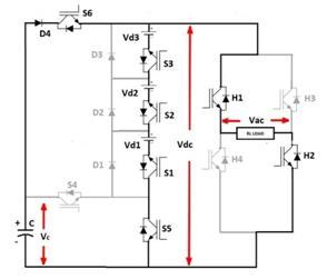
The proposed switched capacitor multilevel inverter circuit is shown in Figure 1.
It is a cascaded MLI setup that is the whole circuit can be divided into two sections the level generating section and the inverter section.
The level generation circuit has a set of three voltage switching unit each unit is made up of a circuit which uses a diode, a switch and a DC source to attain a diode clamped switching arrangement [17]. N number of units can be added to the circuit to attain higher levels. The three sources used in the given system are Vdc1, Vdc2 and Vdc3. These sources are in asymmetrical patterns as each source has different voltage level [18]. Along with this three switches S1, S2, and S3 with 3 coupling diodes namely D1, D2, D3 are used who’s switching controls the level formation. Also three other switches S4, S5 and S6 and a diode D4 are seen this circuit elements are used to obtain the SCISPC technique by using a single capacitor. Apart from this a H-bridge inverter with four switches H1, H2, H3 and H4 form the second section which performs the inversion of the positive directional stepped waveform to produce an alternating output [19].
The switches used in the level producing circuit should be capable of withstanding high switching frequency. But on the other hand, the switches in the polarity generating H-bridge circuit don’t need high frequency capability as they operate at the fundamental frequency [20]. The overall operation of the proposed system falls under two modes of operation which is discussed in Table 1.
Figure 1. Circuit structure of the proposed switched capacitor multilevel inverter
Table 1. Switching states of the proposed system
|
SWITCHES |
VOLTAGE |
LEVEL |
|||||||||
|
1 |
0 |
0 |
1 |
0 |
1 |
0 |
1 |
1 |
0 |
84 |
14 |
|
0 |
1 |
1 |
0 |
0 |
1 |
1 |
0 |
0 |
1 |
72 |
13 |
|
1 |
1 |
1 |
0 |
0 |
1 |
0 |
1 |
0 |
1 |
66 |
10 |
|
0 |
0 |
1 |
1 |
0 |
1 |
1 |
0 |
1 |
1 |
42 |
6 |
|
0 |
1 |
1 |
0 |
1 |
1 |
1 |
0 |
0 |
0 |
18 |
5 |
|
1 |
1 |
0 |
0 |
1 |
1 |
0 |
0 |
1 |
1 |
-6 |
-2 |
|
1 |
0 |
0 |
1 |
1 |
1 |
1 |
0 |
0 |
0 |
-12 |
-3 |
|
0 |
0 |
1 |
0 |
0 |
1 |
0 |
0 |
1 |
0 |
-30 |
-5 |
|
1 |
1 |
1 |
1 |
0 |
0 |
0 |
0 |
1 |
1 |
-36 |
-7 |
|
0 |
1 |
0 |
1 |
0 |
1 |
0 |
1 |
0 |
1 |
-42 |
-9 |
The overall operation of the proposed system can be divided into two modes. These modes are discussed below.
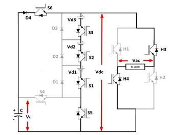
2.1 Mode I (capacitor in parallel connection)
During mode I the diode D4 and switches S5 and S6 are ON while S4 is kept in OFF position this connects the capacitor in parallel configuration as discussed earlier. Now the remaining three S1, S2, and S3 are switched based on the switching patters given in table I. This operation can produce a maximum of 15 level output. Seven in the positive cycle when H1 and H2 are ON in the H-bridge circuit shown in Figure 2(a). Seven levels in the negative cycle when H3 and H4 are in ON shown in Figure 2(b). And the zero level was also taken in account thus making a total of 15 levels. The operation of the circuit in this mode and its current direction is shown in below Figure 2. The level generator’s output is given by the Eq. (1)
$V_{d c}=\left(V_{d 1} * S_{1}\right)+\left(V_{d 2} * S_{2}\right)+\left(V_{d 3} * S_{3}\right)$ (1)
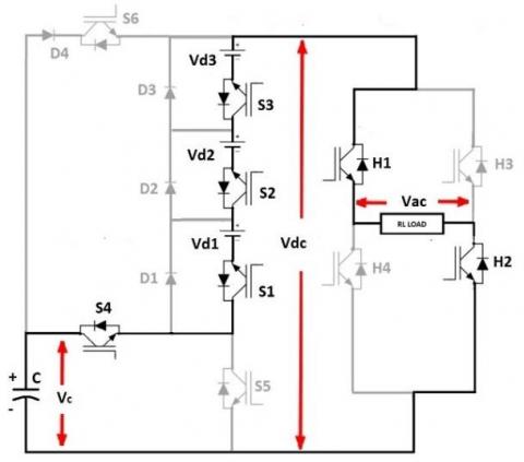
2.2 Mode II (capacitor in series connection)
During Mode II the diode D4 and switches S5 and S6 are turned OFF leaving the switch S4 in ON state. This switching pattern connects the capacitor in series with other sources. Now by following the same switching pattern another set of 15 voltage steps can be formed at even higher voltage level as the capacitor voltage gets added to the already available voltage sources.
(a) Circuit operation for positive half cycle at max DC output level in Mode I
(b) Circuit operation for positive half cycle at max DC output level in Mode I
Figure 2. Circuit operation modes
Figure 3. Circuit operation for positive half cycle at max DC output level in Mode II
This produces 7 levels above the previous 7 levels in positive half cycle when H1 and H2 are ON and 7 levels below the previous 7 levels in the negative half cycle when H3 and H4 are in ON state. Thus a total of 31 level output waveform can be produced without the use of any additional DC sources are components. The operation of the circuit in mode II in both positive cycle and negative half cycle is shown in Figure 3.
Level voltage output at mode II is given by Eq. (2)
$V_{d c}=\left(V_{d 1} * S_{1}\right)+\left(V_{d 2} * S_{2}\right)+\left(V_{d 3} * S_{3}\right)+\left(V_{c} * S_{4}\right)$ (2)
The number of switches used in the level generation circuit is denoted by the variable ‘Ls’ and the number of voltage level produced is denoted by ‘Lv’. The switches and the levels can be related by the below Eq. (3).
$\mathrm{L}_{\mathrm{s}}=\mathrm{L}_{\mathrm{v}}=(2 \mathrm{n}+1) 2$ (3)
where, n = 3, ‘n’ is the number of switches used in the level generation circuit
The total number of levels at the output load is denoted by ‘Lf’ given by Eq. (4).
$\mathrm{L}_{\mathrm{f}}=2 \mathrm{L}_{\mathrm{s}}+1$ (4)
The final voltage steps after the inverter can be calculated using Eq. (5)
$\mathrm{V}_{\mathrm{ac}}=\mathrm{V}_{\mathrm{dc}}\left(\mathrm{H}_{1}-\mathrm{H}_{3}\right)$ (5)
Figure 4. Output waveform of proposed system
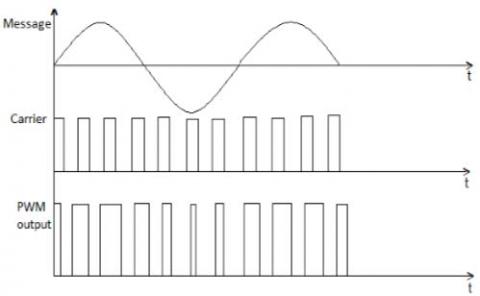
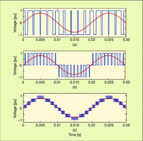
In multi carrier SPWM based pulse generation method multiple number of triangle carrier waves are compared with a single sinusoidal reference waveform to produce the require pulse [21]. Here the amplitude and the frequency of all carrier are same but the positions are manipulated based on the width of the final PWM signal. This method produces a pulse whenever the amplitude reference waveform which oscillates at fundamental frequency ie.50Hz and its zero reference placed at the middle of this carriers is greater than the carrier amplitude. For an MLI circuit with ‘n’ levels we need n-1 number of triangular carriers [22]. The output waveform of the proposed system is depicted in Figure 4. The resultant pulse is summed up and given to the inverter to obtain the desired steps in the output waveform. Though it is a simple method the output levels produced by applying this pulse to the inverter has internal chopping this causes higher switching losses any may reduce the life time of the inverter. This drawback has been rectified by the application of Selective Harmonics Elimination as discussed in III (a). The below Figures 5(a) and 5(b) shows output wave form of a 29 level inverter which uses Multicarrier SPWM based control technique.
(a) carrier and reference comparison plot with 14 carrier
(b) output waveform of a 31 level inverter which uses multicarrier SPWM
Figure 5. Reference comparison and output waveforms
The procedure of the proposed work has been verified through MATLAB/ SIMULINK software platform. The same is also experimentally verified by using DSPIC30F2010 controller.
Figure 6. Proposed system MCM comparison
Figure 6 shows the shows the Multi carrier signal for controlling the proposed thirty one level inverter, fifteen carrier signal and one reference signal.
Figure 7. Proposed system PWM pulse to the H bridge inverter
Figure 7 shows PWM pulses for controlling the H bridge inverter with 180 degree mode of conduction.
Figure 8. Proposed system PWM pulse to the H bridge inverter
Figure 8 represents the PWM pulse rate to the H Bridge inverter clearly.
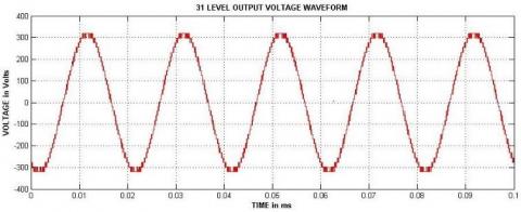
Figure 9. Proposed system thirty one level inverter output voltage
The proposed method system thirty one level inverter output voltage is represented in Figure 9.
Figure 10 Represents proposed system thirty one level inverter output current levels.
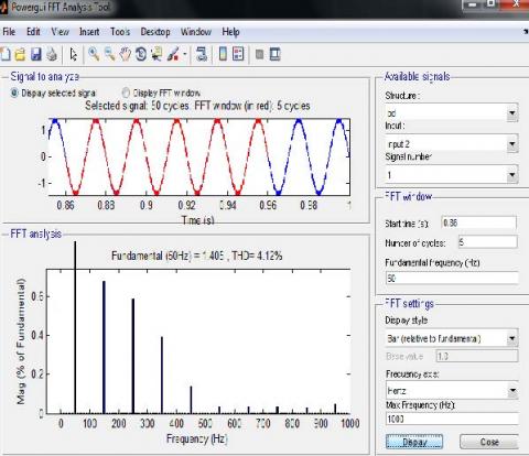
The Proposed system thirty one level inverter THD levels are illustrated in Figure 11.
Figure 10. Proposed system thirty one level inverter output current
Figure 11. Proposed system thirty one level inverter THD
Figure 12. Hardware result of DC voltage to the multilevel inverter
The Hardware result of DC voltage compared to multilevel inverter is depicted in Figure 12.
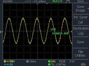
Figure 13. Hardware result of thirty one level inverter output voltage waveform
The Figure 13 indicates the hardware result of thirty one level inverter output voltage waveform.
Figure 14. Experimental setup
The above figure 14 shows the experimental setup for proposed reduced switch thirty one level inverter developed using DSPIC30F2010 controller.
A novel single phase asymmetrical multilevel inverter topology which uses SCISPC method is proposed. The inverter has two set of circuits the level generator and H bridge inverter arranged in a cascaded set up. A multi carrier PWM studied and applied to obtain the desired results with lower harmonics and switching losses. A switched capacitor based series parallel control was also used to obtain higher voltage levels with reduces DC sources. The simulation and experimental results were discussed elaborately in this paper. To test the feasibility of this system a hardware prototype was developed which uses DSPIC controller to generate the switching pulse’s at desired angles.
[1] Zamiri, E., Vosoughi, N., Hosseini, S.H., Barzegarkhoo, R., Sabahi, M. (2016). A new cascaded switched-capacitor multilevel inverter based on improved series–parallel conversion with less number of components. IEEE Transactions on Industrial Electronics, 63(6): 3582-3594. https://doi.org/10.1109/TIE.2016.2529563
[2] Raghu Raman, S., Cheng, K.W.E., Ye, Y.M. (2018). Multi-input switched-capacitor multilevel inverter for high-frequency AC power distribution. IEEE Transactions on Power Electronics, 33(7): 5937-5948. https://doi.org/10.1109/TPEL.2017.2742525
[3] He, L.Z., Cheng, C. (2016). A flying-capacitor-clamped five-level inverter based on bridge modular switched-capacitor topology. IEEE Transactions on Industrial Electronics, 63(12): 7814-7822. https://doi.org/10.1109/TIE.2016.2607155
[4] Babaei, E., Gowgani, S.S. (2014). Hybrid multilevel inverter using switched capacitor units. IEEE Transactions on Industrial Electronics, 61(9): 4614-4621. https://doi.org/10.1109/TIE.2013.2290769
[5] Liu, J.F., Wu, J.L., Zeng, J. (2012) Symmetric/asymmetric hybrid multilevel inverters integrating switched-capacitor techniques. IEEE Journal of Emerging and Selected Topics in Power Electronics, 6(3): 1616-1626. https://doi.org/10.1109/JESTPE.2018.2848675
[6] Lee, S.S., Sidorov, M., Lim, C.S., Idris, N.R.N., Heng, Y.E. (2018). Hybrid cascaded multilevel inverter (HCMLI) with improved symmetrical 4-level sub module. IEEE Transactions on Power Electronics, 33(2): 932-935. https://doi.org/10.1109/TPEL.2017.2726087
[7] Babaei, E., Laali, S., Bayat, Z. (2015). A single-phase cascaded multilevel inverter based on a new basic unit with reduced number of power switches. IEEE Transactions on Industrial Electronics, 62(2): 922-929. https://doi.org/10.1109/TIE.2014.2336601
[8] Mariethoz, S. (2013). Systematic design of high-performance hybrid cascaded multilevel inverters with active voltage balance and minimum switching losses. IEEE Transactions on Power Electronics, 28(7): 3100-3113. https://doi.org/10.1109/TPEL.2012.2222446
[9] Zambra, D.A.B., Pinheiro, J.R. (2013). Comparison of phase-shift and step wave modulation technique applied to symmetrical cascaded multilevel inverter. IEEE Latin America Transactions, 11(5): 1156-1162. https://doi.org/10.1109/TLA.2013.6684389
[10] Hasan, M.M., Abu-Siada, A., Dahidah, M.S.A. (2017). A three-phase symmetrical DC-link multilevel inverter with reduced number of DC sources. IEEE Transactions on Power Electronics, 33(10): 8331-8340. https://doi.org/10.1109/TPEL.2017.2780849
[11] Su, G.J. (2005). Multilevel DC-link inverter. IEEE Transactions on Industry Applications, 41(3): 848-854. https://doi.org/10.1109/TIA.2005.847306
[12] Busquets-Monge, S., Rocabert, J., Rodriguez, P., Alepuz, S., Bordonau, J. (2008). Multilevel diode-clamped converter for photovoltaic generators with independent voltage control of each solar array. IEEE Transactions on Industrial Electronics, 55(7): 2713-2723. https://doi.org/10.1109/TIE.2008.924011
[13] Busquets-Monge, S., Griñó, R., Nicolas-Apruzzese, J., Bordonau, J. (2016). Decoupled DC-link capacitor voltage control of DC–AC multilevel multileg converters. IEEE Transactions on Industrial Electronics, 63(3): 1344-1349. https://doi.org/10.1109/TIE.2015.2495295
[14] Adam, G.P., Finney, S.J., Massoud, A.M., Williams, B.W. (2008). Capacitor balance issues of the diode-clamped multilevel inverter operated in a quasi two-state mode. IEEE Transactions on Industrial Electronics, 55(8): 3088-3099. https://doi.org/10.1109/TIE.2008.922607
[15] Yuan, X.M., Barbi, I. (2000). Fundamentals of a new diode clamping multilevel inverter. IEEE Transactions on Power Electronics, 15(4): 711-718. https://doi.org/10.1109/63.849041
[16] Ebrahimi, J., Babaei, E., Gharehpetian, GB. (2012). A new multilevel converter topology with reduced number of power electronic components. IEEE Transactions on Industrial Electronics, 59(2): 655-667. https://doi.org/10.1109/TIE.2011.2151813
[17] Najafi, E., Yatim, A.H.M. (2012). Design and implementation of a new multilevel inverter topology. IEEE Transactions on Industrial Electronics, 59(11): 4148-4154. https://doi.org/10.1109/TIE.2011.2176691
[18] Hinago, Y., Koizumi, H. (2012). A switched-capacitor inverter using series / parallel conversion with inductive load. IEEE Transactions on Industrial Electronics, 59(2): 878-887. https://doi.org/10.1109/TIE.2011.2158768
[19] Tsunoda, A., Hinago, Y., Koizumi, H. (2014). Level- and phase-shifted PWM for seven-level switched-capacitor inverter using series/parallel conversion. IEEE Transactions on Industrial Electronics, 61(8): 4011-4021. https://doi.org/10.1109/TIE.2013.2286559
[20] Choi, J.S., Kang, F.S. (2015). Seven-level PWM inverter employing series-connected capacitors paralleled to a single DC voltage source. IEEE Transactions on Industrial Electronics, 62(6): 3448-3459. https://doi.org/10.1109/TIE.2014.2370948
[21] Sajadi, R., Iman-Eini, H., Bakhshizadeh, M.K., Neyshabouri, Y., Farhangi, S. (2018). Selective harmonic elimination technique with control of capacitive DC-link voltages in an asymmetric cascaded H-bridge inverter for STATCOM application. IEEE Transactions on Industrial Electronics, 65(11): 8788-8796. https://doi.org/10.1109/TIE.2018.2811365
[22] Ahmed, M., Sheir, A., Orabi, M. (2017). Real-time solution and implementation of selective harmonic elimination of seven-level multilevel inverter. IEEE Journal of Emerging and Selected Topics in Power Electronics, 5(4): 1700-1709. https://doi.org/10.1109/JESTPE.2017.2746760