Tianyu Zhang | Yudong Li*
OPEN ACCESS
To ensure the DC-side voltage stability of cascade static synchronous compensator (STATCOM) units, this paper proposes a pulse width modulation (PWM) algorithm based on virtual flux (VF) for model prediction. Firstly, a VF model was established, which predicts the ideal voltage vector under zero VF error, calculates the DC-side voltage per unit and rounds it to the ideal voltage, and determines the module state by balancing the DC-side voltage between the unit modules. Secondly, the author explained the flow of PWM algorithm based on VF-tracking, and analyzed the waveform features. Finally, the proposed PWM algorithm was applied to the STATCOM of cascade multi-level converter. The results of simulation, field experiment and analysis show that the VF-based PWM algorithm for the model prediction of cascade STATCOM can achieve good modulation effect and strike a balance of DC-side voltage between the unit modules. Thus, the proposed PWM algorithm is both rational and feasible.
cascade static synchronous compensator (STATCOM), reactive power compensation (RPC), pulse width modulation (PWM), virtual flux (VF), DC-side voltage balancing
With high permeability and intermittency, renewable energy generation has been widely used in the third-generation grid. After the renewable energy power is connected to the grid, it is imperative to enhance reactive power compensation (RPC) and voltage control [1]. One of the most popular RPC options is cascade static synchronous compensator (STATCOM), an advanced dynamic RPC device with continuous output, small harmonics and fast adjustment [2]. As its name suggests, the cascade STATCOM consists of a cascade of unit modules. The special structure has aroused much interest in its modulation strategy and the balancing of capacitor voltage between the modules [3-16].
Some scholars have improved and simplified the complex modulation strategy facing multiple levels, failing to apply the strategy in the STATCOM. For example, Reference [5] proposes a new carrier phase-shift modulation strategy that requires a few pulse width modulation (PWM) generators in digital implementation. References [6-7] discuss the simplified space vector modulation strategy for cascaded H-bridge converter.
Some scholars have developed modulation strategies that balance the DC-side capacitor voltage of the module through closed-loop control, which is easy to implement when there are many modules, but faces complicated selection of control parameters and coupling between the control links. For instance, Reference [8] develops a cascaded multi-level structure for the RPC, which controls the converter by a step-wave modulation method with selective harmonic elimination (SHE), and explores the way to balance the capacitor voltages between the modules. To ensure the modulation effect under a few modules, Reference [9] suggests applying carrier phase shift modulation (CPSM) in cascade STATCOM, and analyzes the effects of DC-side voltage fluctuation on the modulation. Targeting cascade STATCOM under the CPSM, References [10-11] put forward a three-stage balancing plan for the capacitor voltages between the modules, aiming to balance the AC-side voltage between the modules and phases. Reference [12] looks for the causes of power imbalance between the modules under the CPSM, and uses carrier rotation to reduce the effects of the modulation strategy on power balance control between the modules. References [13-14] investigate how the balancing of AC-side voltage between the modules affects the upper-layer control of the system under the SHE and the CPSM, respectively, and set up a control algorithm based on the small-signal model to weaken the coupling effect.
Considering the importance of DC-side voltage stability to cascade STATCOM modulation, some scholars have tried to maintain the stability of DC-side voltage through DC-side voltage ranking, which is effective and easy to implement digitally. Reference [15] combines digital and analog controls to modulate cascade H-bridge rectifier and balance DC-side capacitor voltage. Reference [16] simplifies the phase disposition modulation such as to balance the DC-side voltage through ranking. Integrating deadbeat control into the cascade STATCOM, References [17-18] balance DC-side capacitor voltage through ranking and employs model estimation control to balance capacitor voltage, constrain switch frequency and minimize system losses.
To maintain the DC-side voltage stability and improve the dynamic/static control of cascade STATCOM units, this paper establishes a simplified algorithm of PWM model estimation for cascade STATCOM in light of the results in References [19-20]. Specifically, the switch state of the converter was determined through virtual flux (VF) prediction, the nearest level approximation and DC-side voltage ranking, while the features of the converter output waveform were analyzed under the control of the proposed algorithm. The proposed algorithm is easy to implement, requires no vector optimization and outperforms ordinary carrier modulation in the utilization efficiency of DC-side voltage.
Firstly, a VF prediction model was established based on the structure of cascade multi-level converter. This model predicts the ideal voltage vector under zero VF error, calculates the DC-side voltage per unit and rounds it to the ideal voltage, and determines the module state by balancing the DC-side voltage between the unit modules. Secondly, the author explained the flow of PWM algorithm based on VF-tracking, and analyzed the waveform features. Finally, the proposed PWM algorithm was applied to the STATCOM of cascade multi-level converter. The results of simulation, field experiment and analysis show that the VF-based PWM algorithm for the model prediction of cascade STATCOM can achieve good modulation effect and strike a balance of DC-side voltage between the unit modules. Thus, the proposed PWM algorithm is both rational and feasible.
Figure 1. The topology of the cascade STATCOM
The topology of cascade STATCOM is illustrated in Figure 1, where Figure 1(a) presents the single-phase full-bridge circuit and Figure 1(b) shows the circuit diagram of a unit module. In Figure 1(a), ea, eb and ec are the grid voltages at different connection points; ia, ib and ic are the output currents of the STATCOM; L is the reactance of the reactor. In Figure 1(b), C is the DC-side electrolytic capacitor; udcx is the DC-side voltage of the unit module; Vx is the output voltage of module x; sx1, sx2, sx3 and sx4 are the switch state variables of module x. As shown in Figure 1(a), xÎ{a1,a2,…,aN, b1,b2,…,bN, c1,c2,…,cN}x∈{a1,a2,...,aN,b1,b2,..., bN,c1,c2,...,cN}.
The following can be derived from the reference direction in Figure 1(a) and the circuit theory:
$\left[ \begin{matrix} {{u}_{an}} \\ {{u}_{bn}} \\ {{u}_{cn}} \\ \end{matrix} \right]$ $={{L}_{p}}\left[ \begin{matrix} {{i}_{a}} \\ {{i}_{b}} \\ {{i}_{c}} \\ \end{matrix} \right]$ $+\left[ \begin{matrix} {{e}_{a}} \\ {{e}_{b}} \\ {{e}_{c}} \\ \end{matrix} \right]$(1)
where p is the differential operator (p=d/dt); uan, ubn and ucn are the voltages of points a, b and c relative to point n, respectively. Equation (1) is equivalent to the voltage balance equation for stator winding in a virtual AC motor, when the winding resistance of the stator is neglected. Hence, equation (1) can be rewritten as:
$\left[ \begin{matrix} {{u}_{an}} \\ {{u}_{bn}} \\ {{u}_{cn}} \\ \end{matrix} \right]$ =$p\left[ \begin{matrix} \psi _{a}^{*} \\ \psi _{b}^{*} \\ \psi _{c}^{*} \\\end{matrix} \right]$ (2)
where $Ψ_a^* $, $Ψ_b^*$ and $Ψ_c^*$ are VFs equivalent to the stator fluxes of the virtual motor. From equations (1) and (2), it can be seen that the VF control is equivalent to the voltage modulation for the output current of the STATCOM.
The flux-tracking PWM tracks the reference flux circle, i.e. the ideal flux circle of the motor stator, with the actual flux vector generated through the control of the different switching modes of the converter, producing a PWM wave in the tracking process [20]. Targeting the cascade STATCOM, this paper proposes a VF-tracking PWM algorithm that determines the output of each phase of the converter through VF prediction and nearest level approximation, and then ascertains the switch state of each module of the converter according to the DC-side voltage ranking of the unit modules.
3.1 Prediction of ideal voltage vector
The modulated wave voltage can be defined as:
$\left\{ \begin{matrix} {{u}_{a}}=U\sin (\omega t) \\ {{u}_{b}}=U\sin (\omega t-2\pi /3) \\ {{u}_{c}}=U\sin (\omega t+2\pi /3) \\ \end{matrix} \right.$ (3)
where ua, ub and uc are the voltages of the three-phase modulated wave; U is the peak voltage of the modulated wave; ω is the angular frequency of the power supply. Then, the modulated wave voltage in the αβ coordinate system can be expressed in the vector form below:
$u=u_α+ju_β$ (4)
where
$\left[ \begin{matrix} u_{\alpha} \\ u _{\beta} \\ \end{matrix} \right]$=$\frac{2}{3}$ $\left[ \begin{matrix} 1-\frac{1}{2} & \text{-}\frac{1}{2} \\ 0\frac{\sqrt{3}}{2} & text{-}\frac{\sqrt{3}}{2} \\ \end{matrix} \right]$ $\left[ \begin{matrix} {{u}_{a}} \\ {{u}_{b}} \\ {{u}_{c}} \\ \end{matrix} \right]$
Taking the VF under the modulated wave voltage as the ideal flux linkage, the vector equation of the ideal flux in the αβ coordinate system can be expressed as:
$\frac{dψ^*}{dt}=u$ (5)
Discretizing equation (5) with sampling period Ts, we have:
$ψ^* (k)=ψ^* (k-1)+u(k)T_s$ (6)
where
${{\psi }^{*}}(k-1)=\sum\limits_{m=1}^{k-1}{u(m){{T}_{s}}}$
Considering Figure 1(b), the unit module states of the STATCOM can be defined as:
${{S}_{x}}=\left\{ \begin{matrix} 1 & {{s}_{x1}},{{s}_{x4}}on\text{ and }{{s}_{x2}},{{s}_{x3}}off \\ -1 & {{s}_{x1}},{{s}_{x4}}off\text{ and }{{s}_{x2}},{{s}_{x3}}on \\ 0 & {{s}_{x1}},{{s}_{x3}}on\text{ and }{{s}_{x2}},{{s}_{x4}}off \\ {} & {{s}_{x1}},{{s}_{x3}}off\text{ and }{{s}_{x2}},{{s}_{x4}}on \\ \end{matrix} \right.$(7)
Without considering the DC-side voltage fluctuation of each module unit, it is assumed that the DC-side voltage of each unit module has stabilized to a given value. Taking the given DC-side voltage of the unit module for approximate analysis, the output voltage of unit module x can be expressed as:
$V_x=S_x u_"dc" ^*$ (8)
where, $u_dc^*$ is the given DC voltage of the unit module. As shown in Figure 1(a), the STATCOM output voltages of points a, b and c relative to point o can be expressed as:
$v_yo∈{0,±u_"dc" ^*,±2u_"dc" ^*,...,±Nu_"dc" ^*} $(9)
where y can be a, b or c. According to the circuit theory, the voltages of points a, b and c relative to point n can be expressed as:
$v_{yn}=v_{yo}-\frac{1}{3}(v_{ao} +v_{bo} +v_{co} ) $ (10)
Relative to point n, the voltage vector of the STATCOM output in the αβ coordinate system can be expressed as:
$v=\frac{2}{3}({{v}_{an}}+{{v}_{bn}}{{e}^{j\frac{2\pi }{3}}}+{{v}_{cn}}{{e}^{j\frac{4\pi }{3}}})$(11)
Further analysis of equation (11) shows that the voltages of points a, b, c relative to point n or point o have the same voltage vector in the αβ coordinate system. Therefore, the vyo and vyn are considered the same in our VF-tracking algorithm, and denoted as vy. Considering equation (2), the actual VF vector of the STATCOM output voltage in the αβ coordinate system can be discretized by the following equation:
$ψ(k)=ψ(k-1)+v(k)T_s$ (12)
where
${\psi}(k-1)=\sum\limits_{m=1}^{k-1}{\nu(m){{T}_{s}}}$
then, output voltage vector of STATCOM at time k was predicted under the zero error between the actual and ideal VFs at time k, and denoted as the ideal voltage vector. From equations (6) and (12), it can be seen that the ideal voltage vector of the converter at time k can be expressed as:
${{v}^{p}}(k)=\frac{1}{T}{{\psi }^{*}}(k)-\frac{1}{{{T}_{s}}}\sum\nolimits_{m=1}^{k-1}{v(m){{T}_{s}}}$(13)
3.2 Determination of unit module state Sx
The unit module state of cascade STATCOM was determined based on the ideal voltage vector in Section 3.1. In the αβ coordinate system, the ideal voltage vector at time k can be described as:
$v^p (k)=v_a^p (k)+jv_β^p (k) $ (14)
The three-phase ideal voltage corresponding to equation (14) can be expressed as:
$\left[ \begin{matrix} v_{a}^{p}(k) \\ v_{b}^{p}(k) \\ v_{c}^{p}(k) \\ \end{matrix} \right]$ $=\left[ \begin{matrix} 1 & 0 \\ -\frac{1}{2} & \frac{\sqrt{3}}{2} \\ -\frac{1}{2} & -\frac{\sqrt{3}}{2} \\ \end{matrix} \right]$(15)
The three-phase ideal voltage can be rounded to the given DC-side voltage $u^*_dc$ of the unit module as:
$\left[ \begin{matrix} v_{a}^{*}(k) \\ v_{b}^{*}(k) \\ v_{c}^{*}(k) \\ \end{matrix} \right]$ $=\frac{1}{u_{dc}^{*}}\left[ \begin{matrix} v_{a}^{p}(k) \\ v_{b}^{p}(k) \\ v_{c}^{p}(k) \\\end{matrix} \right]$(16)
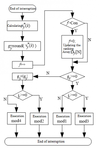
As a result, the module state can be determined according to equation (16) and through the balancing of DC-side capacitor voltage between the modules in each phase of the STATCOM. The determination process is explained in Figure 2 below.
Figure 2. Determination process of unit module state
The predicted voltage $v_y^* (k)$ of each phase can be obtained by equation (16). In Figure 2, round means rounding to the nearest integer; f and Con are the ranking flag variable and ranking flag constant of DC-side voltage, respectively. The modules in each phase should be ranked in ascending order by the DC-side capacitor voltage every Con interruptions, and the corresponding ranks be placed in the array Dy [N]. The smaller the Con, the more frequent the ranking of DC-side voltage. When Con=1, the ranking frequency equals the interruption frequency. The selection of Con must take account of the switching frequency of the device and the requirements on DC-side voltage control. In fact, the value of Con can be determined by simulation. The module states should be assigned according to the output phase voltage vyo of the converter and its corresponding current iy. Here, the four module states are assigned as follows:
$mod1:{S_{D_y [1]}=1,...,S_{D_y [g_y]}=1, S_{D_y [g_y+1}=0,...,S_{D_y [N]}=0}$
$mod2:{S_{D_y [1]}=-1,...,S_{D_y [g_y]}=-1, S_{D_y [g_y+1}=0,...,S_{D_y [N]}=0}$
$mod3:{S_{D_y [1]}=0,...,S_{D_y [N-g_y]}=0, S_{D_y [N-g_y+1}=1,...,S_{D_y [N]}=1}$
$mod4:{S_{D_y [1]}=0,...,S_{D_y [N-g_y]}=0, S_{D_y [N-g_y+1}=-1,...,S_{D_y [N]}=-1}$
In the k-th interruption, the low DC-side voltage should be given priority when the input module is charging, while the high DC-side voltage should be prioritized when the input module is discharging. Taking mod1 for instance, the input model is charging if the output phase voltage of the converter is greater than zero and the corresponding current is less than zero; thus, the modules should be inputted in ascending order of the DC-side voltage. After the state of each module is determined, the switch state of the module can be obtained according to equation (7). The two switch states in state zero should be respectively assigned to the charging and discharging states of a module, so as to balance the power between the devices.
Substituting equation (6) into equation (13), the following can be derived from equation (14):
$\left[ \begin{matrix} v_{a}^{p}(k) \\ v_{\beta }^{p}(k) \\ \end{matrix} \right] $ $\text{=}\left[ \begin{matrix} \sum\nolimits_{m=1}^{k-1}{\left[ u_{a}^{*}(m)-{{v}_{a}}(m) \right]u_{a}^{*}(k)} \\ \sum\nolimits_{m=1}^{k-1}{\left[ u_{\beta }^{*}(m)-{{v}_{\beta }}(m) \right]u_{\beta }^{*}(k)} \\ \end{matrix} \right]$ (17)
In light of equation (15), the three-phase voltage corresponding to the above equation can be expressed as:
$\left[ \begin{matrix} v_{a}^{p}(k) \\ v_{b}^{p}(k) \\ v_{c}^{p}(k) \\\end{matrix} \right]$ $\text{=}\left[ \begin{matrix} \sum\nolimits_{m=1}^{k-1}{\left[ u_{a}^{*}(m)-{{v}_{a}}(m) \right]u_{a}^{*}(k)} \\ \sum\nolimits_{m=1}^{k-1}{\left[ u_{b}^{*}(m)-{{v}_{b}}(m) \right]u_{b}^{*}(k)} \\ \sum\nolimits_{m=1}^{k-1}{\left[ u_{c}^{*}(m)-{{v}_{c}}(m) \right]u_{c}^{*}(k)} \\ \end{matrix} \right]$(18)
Similar to equation (15), the transformation of equation (18) does not take account of the zero-sequence voltage component. Hence, the three-phase voltage is actually the voltages at points a, b, c relative to point o in Figure 1(a). Rounding by equation (16), the voltage in any phase can be expressed as:
$v_{y}^{*}(k)=\frac{1}{u_{dc}^{*}}\left\{ \sum\nolimits_{m=1}^{k-1}{\left[ u_{y}^{*}(m)-{{v}_{y}}(m) \right]+u_{y}^{*}(k)} \right\}$ (19)
It can be seen from equation (19) that:
$v_{y}^{*}(k\text{-}1)=\frac{1}{u_{dc}^{*}}\left\{ \sum\nolimits_{m=1}^{k-2}{\left[ u_{y}^{*}(m)-{{v}_{y}}(m) \right]+u_{y}^{*}(k-1)} \right\}$ (20)
Finding the difference between the above two equations, we have:
$v_{y}^{*}(k)=v_{y}^{*}(k-1)\text{+}\frac{1}{u_{dc}^{*}}\left[ u_{y}^{*}(k)\text{-}{{v}_{y}}(k-1) \right]$ (21)
Without considering the DC-side voltage fluctuation of the unit module, the given DC-side voltage can be adopted for further analysis:
$v_y (k-1)=round[v_y^* (k-1)]⋅u_{dc} ^{*} $ (22)
From equations (21) and (22), we have:
${{v}_{y}}(k)=round\left\{ v_{y}^{*}(k-1)-round\left[ v_{y}^{*}(k-1) \right]+\frac{u_{y}^{*}(k)}{u_{dc}^{*}} \right\}\cdot u_{dc}^{*}$ (23)
Through the analysis on equation (23), it can be seen that only one module belongs to the PWM state, while all the other modules are in the step wave state, for the phase y output voltage is or at; the voltage difference of the PWM wave at time k and time k-1 peaks at under VF tracking.
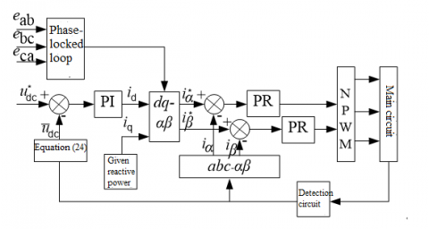
5.1 Cascade STATCOM control strategy
The VF-based simplified PWM was integrated with DC-side voltage and current control, and applied to cascade STATCOM. The block diagram of the cascade STATCOM control is presented in Figure 3, where the voltage loop is under proportional integral control, is the given DC-side voltage of a module, and is the mean voltage of all modules:
$\bar{u}_{dc}=\frac{1}{3N}\sum u_{dcx}$ (24)
where N is the number of modules in each phase. The active component of the STATCOM can be obtained by PI control over the mean voltage difference of DC side modules. The α and β components of the current can be determined through the dq-αβ transformation of the active and inactive components. The current loop is regulated by a proportional resonant (PR) controller [22]. The controller outputs the modulated wave for the PWM algorithm.
Figure 3. The block diagram of the cascade STATCOM control
5.2 Algorithm simulation and analysis
To verify the effectiveness of the proposed PWM algorithm, the cascade STATCOM was simulated and analyzed based on the PWM algorithm, using 4 cascade modules and the parameters in Table 1. The DC-side parallel resistances of the four modules in each phase were set to 200Ω, 300Ω, 400Ω and 320Ω, respectively, aiming to simulate the difference in power loss between modules.
Table 1. Key simulation parameters
|
Parameter |
Value |
|
Grid voltage |
3,300 V |
|
Reactance |
2.5 mH |
|
DC-side capacitor voltage of a module |
800/650 V |
|
DC-side capacitance of a module |
5000 uF |
|
Sampling frequency |
20 kHz |
|
Mean switch frequency of a device |
1200 Hz |
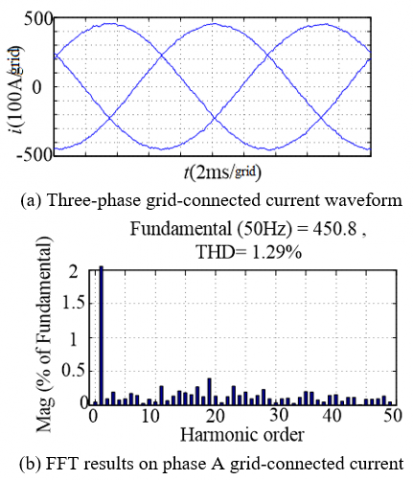
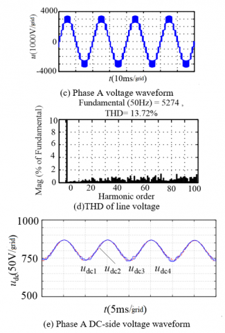
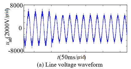
Figure 4 displays the waveform of the STATCOM in the steady state with a compensation capacity of 1,800kVar. Figures 4(a)~4(e) respectively gives the waveform of the STATCOM’s grid-connected current, the fast Fourier transform (FFT) results on the phase A grid-connected current over one period, the phase A voltage waveform outputted by the STATCOM, the FFT results on the line voltage corresponding to the STATCOM output in one period, and the phase A DC-side voltage waveform. It can be seen that the total harmonic distortion (THD) of phase A grid-connected current over one period reached 1.29%; the line voltage corresponding to the STATCOM output in one period had a THD of 13.72%, and the harmonic distribution is relatively scattered; the maximum difference of phase A DC-side voltage was 10V.
Figure 4. Simulated waveform of the steady state
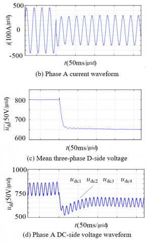
Figure 5 shows the dynamic waveform of the STATCOM, when the output power of STATCOM to the grid changed abruptly from leading reactive 1,800kVar to lagging reactive 1,200kVar, and the given DC-side voltage dropped suddenly from 800V to 650V. Figures 5(a)~5(d) respectively show the STATCOM’s output line voltage waveform diagram, the phase A grid-connected current waveform outputted by the STATCOM, the mean three-phase voltage waveform, and the phase A DC-side voltage waveform. It can be seen that the voltage and current regulation time was less than 5ms according to Figure 5(a); the DC-side voltage took less than 20ms to regulate, while the voltages of different modules were basically balanced in the dynamic process. Overall, the waveforms in Figure 5 demonstrate the good dynamic and static responses of the STATCOM using the VF-based PWM algorithm.
Figure 5. Dynamically simulated waveform
Based on the circuit topology of the cascade STATCOM, a PWM algorithm was established to balance DC-side voltage and track VF. Then, a mathematical model was created for the VF, and the waveform features of the proposed PWM algorithm were analyzed. Finally, the simplified VF-based PWM algorithm for model estimation was verified through simulation analysis, in light of the control method for STATCOM. The results show that the proposed algorithm can regulate the cascade STATCOM, satisfy the control needs for this type of STATCOM, with the aid of DC-side voltage ranking, and achieve high flexibility and easy implementation. The future research will consider the DC-side capacitor voltage fluctuation of unit module, optimize DC-side voltage balancing, and tackle the dead zone of the device during the balancing process.
This work is supported by Open Project of Key Laboratory of Control Engineering of Henan Province (KG2016-05) and Key scientific research project of Henan higher education (Grant No.16A470009).
[1] Zhou XX, Chen SY, Lu ZX. (2013). Historic review and prospect for power systems and related technologies: A concept of three-generation power systems. Proceedings of the CSEE 33(12): 99-106.
[2] Gultekin B, Gercek CO, Atakik T, Deniz M, Bicer N, Ermis M, Köse N, Ermis C, Koç E, Cadirci I, Acik A, Akkaya Y, Toygar H, Bideci S. (2012). Design and implementation of a 154-kV ±50-Mvar transmission STATCOM based on 21-level cascadec multilevel converter. IEEE Transactions on Industrial Applications 48(3): 1030-1045. https://doi.org/10.1109/ECCE.2010.5617795
[3] Vazquez S, Leon JI, Carrasco JM, Garcia Franquelo L, Ramon Galvan E, Reyes M, Antonio Sanchez J, Dominguez E. (2010). Analysis of the power balance in the cells of a multilevel cascaded H-bridge converter. IEEE Transactions on Industrial Electronics 57(7): 2287-2296. https://doi.org/10.1109/TIE.2009.2034679
[4] Yang B, Zeng G, Zhong YR, Zeng G. (2013). DC capacit or voltage balance control strategy of cascade STATCO M based on step wave modulation. Transactions of China Electrotechnical Society 28(10): 280-287. https://doi.org/10.3785/j.issn.1008-973X.2014.04.007
[5] Wang LQ, Qi F. (2010). Novel carrier phase-shifted SPWM for cascade multilevel converter. Proceedings of the CSEE 30(3): 28-34.
[6] Wu FJ, Sun L, Zhao K. (2009). Novel simple multilevel space vector modulation method for cascade inverter. Proceedings of the CSEE 29(12): 36-40. https://doi.org/10.1109/MILCOM.2009.5379889
[7] Zhu SG, OuYang HL, Yan JL. (2012). Research on simplified space vector modulation and performance optimization for cascaded inverter in 45º coordinate system. Transactions of China Electrotechnical Society 27(2): 68-76.
[8] Peng FZ, Lai JS, Mckeever JW. (1996). A multilevel voltage -source inverter with separate DC sources for static Var generation. IEEE Transactions on Industry Applications 32(5): 1130-1138.
[9] Liang YQ, Nwankpa CO. (1999). A new type of STATCOM based on cascading voltage-source inverters with phase-shifted unipolar SPWM. IEEE Transactions on Industry Applications 35(5): 1118-1123. https://doi.org/10.1109/28.793373
[10] Akaka H, Inoue S, Yoshii T. (2007). Control and Performance of a Transformerless Cascade PWM STATCOM With Star Configuration. IEEE Transactions on Industry Applications 43(4): 1041-1049. https://doi.org/10.1109/tia.2007.900487
[11] Liu Z, Liu BY, Duan SX, Kang Y, Shi YJ, Chen ZW. (2009). DC capacitor voltage balancing control for cascade multilevel STATCOM. Proceedings of the CSEE 29(30): 7-12. https://doi.org/10.1109/MILCOM.2009.5379889
[12] Dai K, Xu C, Ding YF, Kang Y. (2013). The applications of carrier rotation modulation on cascaded h-bridge STATCOM. Proceedings of the CSEE 33(12): 99-106.
[13] Liu Y, Huang AQ, Song WC, Bhattacharya S, Tan G. (2009). Small-signal model-based control strategy for balancing individual DC capacitor voltages in cascade multilevel inverter-based STATCOM. IEEE Transactions on Industrial Electronics 56(6): 2259-2269. https://doi.org/10.1109/TIE.2009.2017101
[14] She X, Huang AQ, Zhao T, Wang GY. (2012). Coupling effect reduction of a voltage-balancing controller in single-phase cascaded multilevel converters. IEEE Transactions on Power Electronics 27(8): 3530-3543. https://doi.org/10.1109/TPEL.2012.2186615
[15] Imaneini H, Schanen JL, Farhangi S, Roudet J. (2008). A modular strategy for control and voltage balancing of cascaded h-bridge rectifiers. IEEE Transactions on Power Electronics 23(5): 2428-2442. https://doi.org/10.1109/TPEL.2008.2002055
[16] Xiong QP, Luo A, Shuai ZK, Ma FJ, Li XC. (2013). Research of single-carrier modulation strategy for cascade SVG. Proceedings of the CSEE 33(24): 74-81.
[17] Townsend C, Summers TJ, Vodden JA, Watson AJ, Betz RE, Clare JC. (2013). Optimization of switching losses and capacitor voltage ripple using model predictive control of a cascaded H-bridge multilevel StatCom. IEEE Transactions on Power Electronics 28(7): 3077-3087. https://doi.org/10.1109/TPEL.2012.2219593
[18] Townsend CD, Summers TJ, Betz RE. (2012). Multigoal heuristic model predictive control technique applied to a cascaded H-bridge StatCom. IEEE Transactions on Power Electronics 27(3): 1191-1200. https://doi.org/10.1109/TPEL.2011.2165854
[19] Du ST, Wu XJ, Zhou J, Wang FJ, Yang Y. (2015). A novel algorithm of PWM using virtual flux model prediction. Proceedings of the CSEE 35(3): 688-694. https://doi.org/10.13334/j.0258-8013.pcsee.2015.03.023
[20] Zhou J, Zhang Y, Geng YW, Wu XJ. (2012). An improved proportional resonant control strategy in the static coordinate for four-leg active power filters. Proceedings of the CSEE 32(6): 113-120.