Gülhan Ustabaş Kaya![]()
© 2024 The author. This article is published by IIETA and is licensed under the CC BY 4.0 license (http://creativecommons.org/licenses/by/4.0/).
OPEN ACCESS
The communication between the lines and contacts on the printed circuit boards (PCBs) is provided by the applied current flow. Due to thermal stress occurring in PCBs exposed to high currents, short-circuit faults (SCF) occur in PCB paths. During a quality PCB inspection before mass production, the initial occurrence time (IOT) of faults should be determined to intervene them at the earliest stage. PCBs are technological wastes that are difficult to recycle due to the diversity of material components and their difficulty of separation. By detecting the IOT of SCF at an early stage, the PCBs production can become recyclable without scrapping. Thus, the amount of PCB waste due to faulty production will be reduced. This paper proposes to diagnose the IOT of SCF that occur when currents (i.e., 8, 11.5, 13.5 Ampere) are applied to PCB paths. This process is performed using a hybrid optical imaging sensor (HOIS) in which lateral shearing digital holographic microscopy (LSDHM) is adapted to microscopic fringe projection profilometry (MFPP). In fault detection with MFPP, which is a surface detection method, the required illumination is provided by LSDHM. In thermal-based SCF diagnosis, a minimum of 36 seconds is required to reach the desired temperature (thermal saturation) for imaging while in optical inspection methods; additional time is required for the polarization process. In conventional methods, faults detection can be performed after only a visible PCB damage is occurred. In contrast, we detect the IOT of SCF in a short time of 1.1 seconds, eliminating the requirement of thermal saturation or polarization. Thanks to the HOIS, since faults are detected at an early stage, damage to the entire PCB will be prevented by repairing the faulty area before mass production.
printed circuit board, short circuit fault, lateral shearing digital holography, microscopic fringe projection profilometry, hybrid optical imaging sensor, early fault detection
Printed circuit boards (PCBs) are the main carriers that provide the electrical connections of devices containing electronic components in the electronic industry [1]. PCBs are a non-conductive substrate plate that mechanically holds various electronic parts together. The assembly and interconnections of electronic components are made on this substrate. This makes it easier to identify and maintain electronic equipment and systems. In addition, circuit properties can be protected with PCBs without causing any changes in inter-circuit capacitance and parasitic effects [2]. PCBs are used in almost all kinds of electronic products e.g., smart watches, phones, communication systems boards, computers and, industrial machines. With the rapidly developing technology, efforts to turn electronic devices into compact devices and bring them to portable sizes have accelerated. To make devices in portable sizes, PCB sizes in integrated circuits should also be produced in very tiny sizes. However, during the rapid production process of very small or complex PCB boards, various PCB faults (visible or invisible) i.e., copper splashes, minimum spacing violation, via-path disconnection, plugged and missing holes, defects of breaks in paths, faulty of copper thickness, rough copper lines, open-circuit failure, short-circuit failure, over and under etch may occur. If this PCB faults cannot be detected precisely in early stage of mass production, most of the produced PCB boards may be scrapped. Therefore, before the mass production process of the PCB, all possible PCB faults should be detected without damaging the entire board. In this context, highly accurate automatic detection devices are needed to detect PCB faults at an early stage [3-6].
Electrical testing (ET), manual visual inspection (VSI), and optical inspection are the most common methods used to detect faults in PCBs [7]. In electrical testing methods, to detect faults in bare PCBs, an observation is required by experts. Not only this method is a non-contact and non-automatic method, but also it requires expensive molds and equipment [8]. Likewise, in manual visual inspection method, a manual observation of workers is also required. This method is not preferred because the detection stability is poor and the probability of false detection is very high. On the other hand, the optical inspection (OI) method has several superior advantages over ET and VSI. With OI, a non-contact inspection method, PCBs can be scanned quickly and faults can be detected with high accuracy [2].
In aforementioned methods, in general, structural PCB faults are detected and focused on faults in component interconnections. With these methods, high current/voltage and temperature-related structural faults on the PCBs have not been examined. Whereas, it has great importance to monitor structural defects due to high current and temperature. Because, the communication between lines and contacts in PCBs is provided by current flow. A Joule's heat is released when current flows through these thin circuit lines on PCBs or the parts mounted on them. This heat causes thermal stress that deforms PCB paths and assembled parts. In this case, it can be said that the temperature occurring due to high current is one of the parameters. These parameters affect the structural health of an equipment or component on a circuit [9-11]. It is also important for PCB quality to diagnose the short circuit faults caused by high current in the paths that provide the connection between the components on the PCB. To detect high current and temperature-related faults in PCBs, thermal imaging and infrared thermography (IRT) are the most common methods [12, 13]. However, with these methods, the high current and temperature faults can be determined only after the PCB is damaged. Therefore, it is not suitable for early fault detection before mass PCB production. On the other hand, the paths in PCB circuits that will operate under high current and voltage have different maximum/minimum current/voltage operating ranges. Therefore, the time of deformation occurs in different paths of the PCB depends on the amount of current. If the IOT of the invisible deformation can be visualized, the malfunction can be intervened without damaging the PCB. Thus, the parts on the PCB can be protected properly. It is not possible to see the IOT of the SCF with thermal imaging and IRT.
On the other hand, since contact methods damage the target surfaces, non-contact PCB inspection methods are preferred that prevents the waste of electronic components in the control process of PCBs. However, non-contact PCB inspection methods require an additional image-processing algorithm or complex/expensive imaging systems to capture high-contrast brightness images for obtaining distinguishable surface roughness and geometric shape characterization.
In order to diagnose the IOT of SCF on PCB path, we propose using hybrid optical imaging sensor (HOIS). The camera used in this system, which can take continuous fast shooting, visualizes the IOT of faults. Thanks to this camera, images with high contrast and brightness can be obtained. While capturing images with the camera, there is no need for additional processes such as polarization because recording is automatically synchronized with the current applied to the PCB path. Whereas thermal imaging and IRT methods require thermal saturation to detect thermal stress caused by high current/voltage and temperature, HOIS eliminates this requirement.
The contributions of this paper are as follows:
We propose HOIS to detect IOT of SCF. Firstly, since the HOIS is a non-contact method, it provides very high accuracy in fault detection compared to expert-based systems. Besides, it eliminates expert workers requirement in diagnosis stage.
Secondly, compared to other non-contact diagnosis methods, i.e., optical-inspection methods, HOIS is a very simple and easy to implement. In addition, HOIS does not require additional algorithms to capture high-contrast brightness images. Besides, unlike optical-based fault detections systems, HOIS does not require polarization/synchronization. Therefore, HOIS is robust against polarization/synchronization errors and initial fault detection time (a.k.a., latency) is shortened.
In addition, compared to thermal-based fault detection systems, HOIS-based fault detection can detect invisible faults at early stage whereas thermals-based fault detection systems can diagnosis visible faults only after the PCB is damaged. Therefore, PCB faults can be determined and repaired before the mass production by HOIS-based system while with the thermal-based system, PCBs turns out to be electronic waste if there is a fault. Furthermore, thermal-based faults detection systems require a saturation time to measure temperature that causes an initial latency (e.g., 36 seconds) but the proposed HOIS-based system can detect faults without any delay.
Lastly, compared all previous methods, the proposed HOIS-based system can determine the IOT of SCF. Therefore, the PCB can be repaired and the mass production process can be resumed. Besides, HOIS-based system can distinguish IOT of SCF based on the current amount on each path that is not possible in all previous methods.
The rest of paper is organized as follows:
The comprehensive literature review related with short-circuit fault diagnosis in PCB are provided in Section II. The related conventional methods, which examined the temperature occurring due to high voltage/current faults, are defined and compared with the proposed HOIS system in this section. In Section III, the materials and methods of the proposed system are defined in detail, including the properties of PCB specimen used in the experiment, working principle of experimental detecting system. In addition, the stages of recording the holographic patterns obtained to display the relevant PCB faults are explained in detail both schematically and mathematically. Section IV presents the experimental results and evaluations. Finally, in Section V, the conclusion is encapsulated and future research directions are proposed.
Detecting the temperature caused by high voltage/current and the faults caused by this temperature at an early stage is one of the best predictive maintenance steps for PCB control. Methods such as resistance temperature detectors (RTD), thermocouples, ultrasonic imaging, thermal imaging and infrared thermography (IRT) are the most common methods used to observe temperature-related faults in PCBs. For example, Kim et al. proposed the usage of the resistance temperature detector (RTD) sensor for measuring the accurate temperature on biochip resistance. This RDT is made of copper by using PCB [14]. However, while they measured the temperature on resistance, PCB faults caused by temperature are not displayed. For this reason, the sensor they recommend is not suitable for the control process of the PCB before mass production. On the other hand, a PCB materials-based wireless passive temperature sensor is fabricated by Yan et al. In this sensor, a resonant cavity with dielectric loaded originating from the PCB substrate is used to detect the temperature [15]. The resonance cavities they used in their proposed study can provide information about surface distortions (faults) on PCB paths. However, instead of examining PCB faults, they only determined the temperature. In another study, the temperature is measured by using a wirelessly-powered embedded system fabricated by Nerone et al. 6 type-K thermocouples can be integrated to digital converters in this embedded system [16]. Although, thermocouples and resistive temperature detectors (RTD) are suitable for measuring temperature, they do not allow non-contact measurement. Moreover, since these methods only allow temperature measurement, they are not suitable for imaging and detecting faults on PCB surfaces or paths. Furthermore, since these systems require very high operating temperatures, they cause damage to PCBs. The damaged PCB has to be scrapped as it cannot be recycled due to the diversity of material components and the difficulty of separating them. PCB waste is an undesirable situation in the electronics industry in terms of cost. Therefore, there is a great need to develop a non-contact sensor that can detect PCB faults caused by high current/voltage before mass production without highoperating temperatures requirement. To address these limitations, we propose HOIS, a non-contact sensor. Since the IOT of SCF can be detected with HOIS, the PCB will not be exposed to high temperatures. In addition, since the IOT of SCF will be detected with HOIS, the PCB will not be exposed to high temperatures. The current/voltage applied to the fault will be terminated as soon as the onset of the fault is detected and the fault in the relevant area can be eliminated without damaging the entire PCB.
Non-contact imaging of multilayer PCBs can be done with ultrasonic imaging, without requiring very high temperatures [17, 18]. The disadvantage of ultrasonic imaging is that the requirements of high thickness and curvature of the PCBs surface for the defects to be visualized. While there is no need to combine the structure with certain substances such as water in the air-coupled ultrasonic Non-destructive testing (NDT) method, information loss occurs in the amplitude of the signal/image due to the high impedance difference between the sample structures and the air [19]. Other methods are preferred for this purpose, as the ultrasonic NDT method is relatively immature for PCB faults due to high current/voltage (such as temperature-induced path distortions) in PCB. Short-circuit defects in PCBs caused by excessive temperature due to high current/voltage can be visualized by different techniques [20]. Thermal imaging (TI) is one of the most widely used of these techniques [12].
On the other hand, infrared thermography (IRT), which can make fast and non-contact measurements, has replaced thermal imaging systems since they are less automatic than optical and X-ray systems [13]. For instance, Swiderski used lock-in thermography as a dynamic thermal imaging detection to improve the sensing nature of infrared thermal imaging and to detect the damage area early in composite materials [21]. Straube and Breitenstein investigated the effect of modulated frequency on Lock-in thermography and visualized the defects in PCB boards [22]. However, in this method, the system delay time needs to be adjusted to solve the synchronization problem between the halogen lamp and the laser signal. Namely, a long detection time requires. Otherwise, the amplitude and phase contrast of the locked thermographic image will be affected [23]. The synchronization problem in IRT technology arises from the use of 2 different sources for illumination. However, in the proposed HOIS, the illumination of the area to be displayed is done only with a laser source. Thus, both the synchronization problem and the additional time required to detect the fault are automatically eliminated. In addition, since the phase and amplitude information will be reconstructed from the captured holographic images with HOIS, 3 dimensional (3D) information of the object can be extracted.
With IRT imaging, defects on the PCB surface are not directly visualized and IRT is not sensitive to contrast. In this method, the heat radiation difference (temperature changes) between the defect area and the back ground is only displayed. For this reason, complementary imaging systems are needed for imaging with IRT technology. In this context, the holographic interferometry and the graphic image processor are combined for imaging the thermal deformation pattern by Netsu et al. [10]. The proposed method is called as Holographic Pattern Measuring System (HPMS). On the other hand, the thermal model of the PCB, which is deformed due to thermal stress, was obtained by using the FEMLAB simulator and thermography together [10]. Georges et al. [24] presented a system where the thermography at infrared wavelengths and holography are combined. To image the temperature and surface shape simultaneously, holographic interferometry based on micro bolometer arrays is combined with CO2 laser. Li et al. [25] designed a multi-sensor image acquisition system to detect the defects in PCBs. In the system they propose, brightness intensity and polarization are recorded with a visible polarization imaging sensor, while infrared intensity is monitored with thermal camera. However, more than one sensor is needed to obtain the images of visible brightness intensity, polarization and infrared intensity simultaneously. This situation creates a problem in terms of cost. Cong et al. [26] aimed to detect the PCBs defects by using optical/thermal fusion imaging system. The characteristic images of lock-in thermography are fused with the images obtained via optical imaging system. On the other hand, in this study, visible optical and infrared images are fused to achieve accurate results. In the merging process, six fusion algorithms are needed. Wang et al. [27] used laser-induced lock-in thermography to detect multiple types of defects in PCBs. Phase characteristic images obtained from optical images are used to detect micro structured defects. In addition, based on a sinusoidal modulation laser, a thermal-wave diffusion model is built to simulate four-layer PCBs. Alaoui et al. [28] used infrared thermal signature to detect faulty capacitors under short circuit and overstressed components in PCBA. In their proposed study, thermal images were captured with an infrared camera, while heat variations were created with capacitors mounted on a DC/DC boost converter board.
In the existing literature, the studies carried out to detect structural PCB failures such as component failures on the PCB. Moreover, applications have been performed by using combined systems to visualize the heat radiation map (temperature changes) created when current flows from the parts mounted on the PCBs or the circuit paths on them. It can be clearly seen that studies of combined systems with thermal imaging -especially using infrared thermography- have more advantages than other methods. However, the required time for the PCB to thermally saturate in the thermal measurement is a disadvantage. Moreover, the detection sensitivity of the recorded images decreases due to uneven brightness levels. Since this method is not sensitive to contrast, additional operations such as polarization are needed to characterize the surface roughness and geometric shape. In addition to all these, it seems that not enough work has been performed to diagnose the initial occurrence time of short-circuit faults on PCB path caused by high current at early stage.
To address these limitations, we propose the usage of a hybrid optical imaging sensor (HOIS). HOIS provides a non-contact measurement. It is composed of the lateral shearing digital holographic microscopy (LSDHM) [29, 30] and the microscopic fringe projection profilometry (MFPP) [31, 32]. To detect IOT of SCF on PCB path with HOIS, illumination with a single light source is sufficient. Since it does not require an additional lighting source, it eliminates the synchronization problem that may occur between the camera and the light source that provides detection. Since the brightness of the surface to be illuminated is provided by the LSDHM arm in HOIS, there is no need for additional processes such as polarization. The brightness is distributed equally to every point of the surface to be detected. Hence, the detection sensitivity of the recorded images increases. In addition, the recorded holographic images contain phase and amplitude information and the 3D information of the detected area can be obtained from this information. Thus invisible faults can be easily detected. On the other hand, there is no need for any temperature to reach saturation when detecting errors. With these aspects, it is superior to all methods available in the literature. It also allows early diagnosis of IOT of SCF caused by high current/voltage on the PCB path. Thanks to early diagnosis, PCB waste can be prevented by early intervention in the faulty area. It will allow rapid and automatic fault checks required before PCB mass production. HOIS was used to detect and classify the micro-size defects in printed circuit board in our previous study and high performance results were obtained [6]. In this work, it will be used to diagnose IOT of SCF on PCB paths caused by high current.
3.1 Specimens
The sample PCB used for fault detection in this study is presented in Figure 1. In this figure, the front (detection) surface of PCBs specimen is shown. This PCB is manufactured by impregnating FR4 copper-plated printed circuit board raw material with epoxy resin by hot pressing, using a non-alkali glass fiber cloth. FR4 is the most commonly used PCB material in printed circuit board production. It has high mechanical and electrical properties and good heat and moisture resistance. Due to these features, the PCB was produced to design a motor driver control card in a battery-powered locomotive. The example PCB shown in Figure 1 is a 70 micron thick copper-coated laminate plate. Its thickness is 1.6mm and it has 2 layers. The size of it 270mm × 250mm × 1.5mm.
Figure 1. The front (detection) surface of the used PCBs specimen
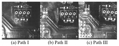
Open circuit and short circuit tests should be performed before mounting electronic materials on each PCB board produced. These tests determine whether the material is defective or not. If PCB faults are detected at an early stage (the IOT can be diagnosed), the produced PCB board will not be discarded as scrap and can be repaired. Otherwise, detecting only visible faults during these tests will not allow the card to be used again. In this context, this study aims to determine the initial occurrence time of short-circuits faults on PCB path during the short circuit test. Experiments are carried out by using 3 paths with the same characteristics (i.e., thickness, length) to prove the early stage detection of short-circuit faults in PCB paths. The length of the paths shown in red circle in Figure 1 are 48.2497mm. The thickness of paths are 0.6350 mm. Electronic components and pins are located in the upper working area of the PCB.
3.2 Experimental detecting system
To diagnose the short-circuit faults (SCF) on PCB path caused by high current, we used the microscopic fringe projection profilometry (MFPP) technique based on lateral shearing digital holographic microscopy (LSDHM). This system is briefly called as the hybrid optical imaging sensor (HOIS). HOIS was used in the previous study for the detection and classification of micro-size defects in the PCBs [6]. It has been suggested to be used in the current study as it has the ability to capture high quality (i.e., high contrast, brightness) image sequences in the desired time interval and to obtain high performance classification results.
On the other hand, in fringe projection techniques, illumination is provided directly by light sources, but it is difficult to accurately adjust the brightness intensity in these systems. For this reason, we adapt the LSDHM system in the part where the light is coming by developing the MFPP technique. By using LSDHM, where the brightness intensity is adjusted appropriately and the temporal phase stability is enabled, a holographic recording medium can be created. With the phase and amplitude information of the holograms captured from the holographic recording medium, the original images can be recovered in 3 dimensional (3D).
The proposed experimental system shown in detail in Figure 2 consists of two arms as detecting and imaging.
Figure 2. The experimental HOIS system
The detecting arm, in which the LSDHM technique is applied, is depicted with bold red circle in Figure 2a. LSDHM not only realizes temporal phase stability in the system, but also allows visualization of invisible faults in micro/nano size. In order to perform the detection process in this arm, the PCB specimen to be tested is placed on the same plane with a recording screen. This screen is called a hologram (interference pattern-IP). To create a hologram, a light source is needed first. In this study, monochromatic Helium-Cadmium (He-Cd) laser was used as the light source with wavelength 442nm and output power 200mW). This light is collimated by using a convex lens 1, which has 100mm focal length. Then it is irradiated to the mirror. By placing the mirror at an angle of approximately 45°, the beam is directed towards to the shear glass plate (SGP), which has 12mm thickness. An interference pattern (IP) is created with the usage of a single SGP. The reason for using SGP is to eliminate the optical component redundancy required in dual-path holographic systems and to eliminate noise caused by vibration. On the other hand, a second lens (Lens 2) is used in this system in order to overcome the DC bias and virtual image problems, which are frequently encountered in holographic systems. The beam from the SGP, which is placed at an angle of approx. 45°, is reflected from Lens 2, creating an effective interference shear area (EISA) in the IP [29].
The mathematical expression of IP with EISA is given in Eq. (1) [6, 30].
$\begin{align} & {{I}_{0}}\left( x,y \right)={{\left| {{O}_{1}}\left( x,y \right)+{{R}_{2}}\left( x,y \right) \right|}^{2}}= {{\left| {{O}_{1}} \right|}^{2}}+{{\left| {{R}_{2}} \right|}^{2}}+O_{1}^{*}{{R}_{2}}+{{O}_{1}}R_{2}^{*} \\\end{align}$ (1)
Here, the half-object beam area is given as $O_1$ and is defined as reflected object beams from the front surface of SGP. It contains target object information. In $R_2$, however, there is no information about the object information. $R_2$ is identified as half-reference beam. To obtain an undistorted real image in reconstruction process and eliminate the real image distortion caused from the spatially varying complex factor, the complex conjugates of $O_1$ and $R_2$ (defined as $O_1^*$ and $R_2^*$, respectively) should be used.
The second arm of the system used in this study is arranged to image the interference patterns of the surface profile created in the first arm. In this context, the setup of the MFPP technique, which is frequently used for the accurate display of surface profiles, has been adapted to the second arm. It is called as imaging arm and shown with dark blue circle in Figure 2a. In this arm, a high-speed digital complementary metal oxide semiconductor (CMOS) camera is used to capture holographic images (interference patterns) of the samples whose information is recorded on the holographic recording plane. CMOS has 512×512 resolution and 14 $\mu m$ × 14 $\mu m$ pixel pitch. The frame rate is 50 frame per second (fps). The software embedded in the CMOS camera is used to set the frame rate of camera, exposure time, trigger mode and other main parameters for real time visualization of the PCBs path faults caused by high current. Magnification is performed by placing a zooming lens on the CMOS to view micro-nano-sized invisible faults. Just in front of the zooming lens is a microscopic objective used for focusing, magnification and contrast imaging. The images recorded on the CMOS camera are transferred to the computer via an interface. Then these holographic images are processed with signal processing techniques.
To explain the proposed system in a basic level, a schematic representation of the experimental setup is presented in Figure 3. In this representation, the location of the LSDHM and MFPP arms is shown in a simpler form. The MFPP arm shown with the blue circle in Figure 3 is the part where PCB faults are imaged with a camera (CMOS) with fast shooting feature. The reason for using a CMOS camera is to view every moment of the change occurring on the PCB path, which is exposed to high current, without interruption during the time. On the other hand, in order to image the PCB surface with MFPP, this surface must be illuminated correctly. For this, LSDHM technique has been adapted to the system. The light was directed with the LSDHM arm created using a light source, a mirror, two lenses and a shearing plate. Additionally, while determining the area of the region desired to be displayed, the required area to be illuminated (EISA) can be determined with this arm.
Figure 3. The schematic representation of HOIS system
In Figure 4, the area illuminated with blue light can be clearly seen. The displayed area is 3 PCB paths with the same properties that have been distorted by exposure to high current. This area is illuminated with blue light. These paths are shown in detail in section 3.1.
Figure 4. The imaging of illuminated PCB area
Our aim in this study is to determine the IOT of SCF on PCB paths depending on the amount of current applied. It also proves that as the amount of applied current changes, the IOT may also change. For this reason, different current amounts were applied to 3 paths with the same characteristics shown in the red circle in Figure 1. In other words, in order not to affect the normal operation of the PCBs, direct current (DC) is applied only to the paths selected as sample. DC is applied separately to the PCB paths with triple output adjustable dc power supply.
In order to apply current to one of the determined paths, two different wires are soldered to both ends of this path. One of the soldered wires is connected to the + end of the DC power supply with the red current probe, while the other is connected to the - end of the DC power supply with the black current probe. (See Figure 4). Then, the DC power supply is turned on and the determined amount of current is given.
In the experiment, firstly, a constant current of 13.5 Amperes (A) is given to the upper path (shown with a red arrow in Figure 1 and numbered I) for 35.56 seconds (s). This path is called as path I. A total of 1778 serial holograms are recorded with the CMOS camera, which has been set to capture 50 frames per second (fps) for a 35.56 s. This means that 1 hologram is recorded in 0.02 s. Namely, the number of recorded holograms has been looked at to determine the IOT of the fault. In the second stage, images (holograms) are captured by applying a constant current of 11.5 A to the bottom PCB path for 300 s (indicated by the green arrow and numerated as III in Figure 1). This path is also named as path III. In the third stage, a variable current from 8 A to 13.5 A is applied to the middle path for 150 s (indicated by the blue arrow and numerated as II in Figure 1) and the series holograms are recorded. This path is called as path II.
In this study, current was applied to each path until a visible deterioration (swelling and burning of the road and smoke) occurred. For this reason, the current duration applied to each path varies. Since the experiment cannot be repeated after swelling occurs in the paths, the experiments have been carried out once per PCB. The experiment is repeated 4 times using 4 mass-produced PCBs with the same features and the same results are obtained each time.
In Figure 5, the raw interference pattern with 512×512 pixel size captured in the absence of any specimen in HOIS is shown.
Figure 5. The raw interference pattern captured in the absence of any specimen
In order to obtain the desired information from the holograms recorded with the HOIS, the phase information related to the height distribution should be extracted. In addition, to measure the change in phase values of fixed points in projection systems, phase deviations called fringe deformation should be converted to height values with a suitable mathematical model [33-35]. In this context, the complex amplitude expression of the interference pattern recorded with LSDHM given in Eq. (1) can be rewritten by considering the MFPP parameters as follows.
$I\left( x,y \right)=2{{I}_{0}}\left( x,y \right)\left\{ 1+\cos \text{ }2\pi \left[ \frac{x}{{{f}_{{{p}_{x}}}}}+\phi \left( x,y \right) \right] \right\}$ (2)
Here, ${{f}_{{{p}_{x}}}}$ is given as in Eq. (3).
${{f}_{{{p}_{x}}}}=\frac{{{f}_{p}}}{\cos \alpha }$ (3)
where, $\alpha$ is the angle between the imaging and detecting arms. ${{f}_{p}}$ is also defined as fringe pitch. The spatial phase $\left( \phi \left( x,y \right) \right)$given in Eq. (4) is constituted with the surface modulation defined on $z=f\left( x,y \right)$ [36].
$\phi \left( x,y \right)=\frac{z\sin \alpha }{{{f}_{p}}}$ (4)
Hilbert transform (HT) [37] was used to reconstruct the image from the holograms recorded with the MFPP system based on LSDHM, whose mathematical expression is given in Eq. (2).
In systems such as MFPP and LSDHM, the very common Fourier transform is generally used when extracting phase information. However, while applying this transformation, redundancies arise due to the Fourier spectra symmetry. In order to eliminate this redundancy in real-valued signals, Hilbert transform is preferred in this study as in the previous study [6]. In addition, in the previous study, it is observed that high performance was achieved by using the phase images obtained by HT.
While obtaining phase information with HT, the expression given in Eq. (4) can be rewritten as in Eq. (5).
$\phi \left( x,y \right)={{\tan }^{-1}}\text{ }\left( \frac{{{I}_{m}}\left( HT\left( {{I}_{x}} \right) \right)}{{{R}_{e}}\left( HT\left( {{I}_{x}} \right) \right)} \right)$ (5)
Based on this phase information, the height information of the imaged PCBs faults, that is, the difference caused by high voltage distortion, can be obtained. The height information given as h is expressed mathematically in Eq. (6).
$h={{f}_{p}}\frac{{{\phi }_{2}}\left( x,y \right)-{{\phi }_{1}}\left( x,y \right)}{2\pi }\frac{\sin \beta }{\sin \alpha }$ (6)
${{\phi }_{1}}\left( x,y \right)$and${{\phi }_{2}}\left( x,y \right)$are the phase of the reference hologram recorded for the non-defective PCB and the phase of the hologram recorded for the faulty PCB, respectively. As for that the $\beta $ angle is the angle between the path of the beam in the LSDHM system and the screen where the hologram recording is made. The obtained 2 dimensional (2D) phase images are called as wrapped phase images that do not contain all of the continuous values. In this study, Goldstein's branch cutting method is used for the phase unwrapping process required to obtain the continuous values [38].
In order to obtain high resolution images with the proposed system, the focus should be done in the most correct way. The calculation process is made by taking into account features such as the magnification ratio of the zooming lens used in the MFPP path, the focal length of the camera, the size of the area to be imaged, the distance of the camera lens to the object, and the camera pixel size [39]. Maximum resolution is achieved when the focal length of the camera lens is set to 450mm. Moreover, when the image size is 512 × 512 pixels and the angle α is (65.77°), the Field of View (FOV) is calculated as 31.00 × 12.00$m{{m}^{2}}$ [40].
In this study, invisible swellings occurring on PCB paths were examined in order to detect short circuit faults at an early stage. Swelling means separation of the metal layer (copper-plated path) from the nonmetal (base PCB material). The temperature resulting from the application of high current causes an internal expansion force on the copper. The pores formed during this expansion create gaps, causing the PCB copper paths to swell. The difference that occurs when a surface is exposed to factors such as temperature and current for a long time does not change after a certain time. This situation is called as saturation [41, 42]. The swelling of the PCB paths reaches saturation due to the high current related increasing temperature and visible distortions occur. In fact, due to high temperatures, burning may occur on the paths and in this case, smoke is observed.
Short circuit faults (swelling in the path) in PCB paths exposed to high current are diagnosed at an early stage by using the HOIS shown in Figure 2. This hybrid sensor is formed by the combination of two different systems. HOIS is based on imaging the illuminated area by using a light source. In this system, Microscopic fringe projection profilometry (MFPP) constitutes the part that detects and displays the faults occurring in PCB paths, while the illumination required during imaging is provided by the lateral cutting digital holographic microscopy system (LSDHM). In Section 3.2, the working principle of this hybrid sensor is explained in detail. Thanks to the integration of LSDHM into MFPP, not only a surface has been imaged, but also micrometer-sized invisible faults can be detected. This allows short circuit faults on invisible PCB paths to be detected at an early stage.
On the other hand, the PCB given in Figure 1 is used as a sample. To display the swelling in the PCB paths, 3 paths with the same characteristics are selected in the sample PCB. Different amounts of current are applied to each path without affecting the normal operation of the PCBs. A three-output adjustable DC power supply is used as the current source. The red current probe attached to the + end of the DC power supply is connected to the wire soldered to one end of the relevant path. The black current probe attached to the - end of the DC power supply is connected to the wire soldered to the other end of the relevant path. (See Figure 4).
Before applying current to the PCB, the PCB is placed at the intersection of the LSDHM path and the MFPP path in the HOIS system. (See Figure 3 and Figure 4). While the LSDHM arm provides illumination of the area to be displayed in the system, it also creates a holographic pattern by creating a holographic recording environment. (See Figure 5). The object to be displayed is placed on this holographic recording medium and by illuminating the object, the information about the object is recorded in the holographic pattern. With the MFPP arm, the created holographic patterns are captured and transferred to the computer via an interface. With the signal processing algorithm whose mathematical expressions are given in detail in Section 3.2, the 3D information of the object (IOT of SCF on the PCB path) is extracted from the holographic pattern.
While extracting 3D information from the holographic pattern, 3D unwrapped phase images obtained from these holograms are used. Phase information of the hologram, which includes the details in the object information, is used to obtain 3D unwrap phase images. While obtaining 3D unwrapped phase images, the phase information of the hologram recorded using the defective PCB is subtracted from the phase information of the recorded hologram using the non-defective PCB.
The 3D unwrapped phase images obtained by using HOIS are used to visualize the initial occurrence time of SCF that vary depending on the amount of current flowing through the PCB path. In this context, the initial occurrence times of the invisible deterioration (swellings) occurring according to the applied current amounts have been examined.
In the first stage of the study, separate reference holograms are recorded for the selected paths without applying any current. The captured reference holograms of the path I, II and III are presented in Figure 6a ,6b,6c respectively.
Figure 6. The recorded reference holograms of Path I, Path II and Path III shown in Figure 1
Detecting faults caused by high current during PCB control before mass production is extremely important to prevent PCB waste. By using thermal cameras and optical inspection methods, which are the most commonly used methods for detecting PCB faults due to SCF related high temperature, only visible faults can be detected. If there is a visible fault, it is very likely that the whole PCB is affected by this faults. In other words, if the faults are visible, the PCB is directly scrapped. However, when the PCB surface or related PCB paths are exposed to high current, current application can be stopped if the damage caused by the current is detected at the beginning. Since this allows the area where the fault occurs to be repaired, the temperature due to high current can be prevented from affecting the entire PCB and other components.
As mentioned above, when a different amount of high current is applied to the identical PCB paths, above the current capacity that can pass over them, the paths will swell. However, when these swellings are not visible, they cannot be detected using traditional methods. In this context, it is proposed to use the HOIS in this study to detect short circuit faults (swelling) in PCB paths exposed to high current at an early stage.
To prove that HOIS is an accurate sensor for this purpose, 3 paths with the same characteristics were determined on the sample PCB used in the study. Different current was applied to each of the paths. Since current is applied to each path until a visible deterioration (swelling, burning and smoke of the path) occurs, the applied current durations are different. As the amount of current increases, the amount of heat generated will also increase. Therefore, swelling formation will accelerate. In addition, as the thickness of the path changes, its resistance due to high current and temperature will also change. Applying current according to the characteristics of the PCB paths will prevent distortions in the PCB. Since this study aims to detect invisible faults at an early stage before swelling occurs, only paths with the same characteristics were examined. For example, 13.5 A is applied to the path called as path I, shown in red arrow in Figure 1. 11.5 A is applied to the path shown in green arrow and called as path III.
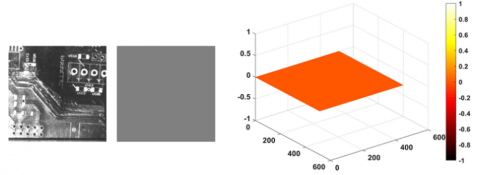
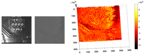
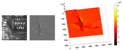
Figure 7 shows the results obtained from the holograms captured when current is applied to paths I and III. In each sub-figure, 3 images are presented as the recorded hologram image, the 2D wrapped phase image reconstructed from this hologram, and the 3D unwrapped phase image reconstructed from the hologram, respectively.
a. Path I with 13.5 A at 0.02 s
b. Path III with 11.5 A at 0.02 s
c. Path I with 13.5 A at 1.1 s
d. Path III with 11.5 A at 1.1 s
e. Path III with 11.5 A at 1.3 s
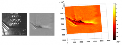
Figure 7. The holograms and their related 2D wrapped and 3D unwrapped phase images for path I and path III at 0.02s,1.1s and 1.3s
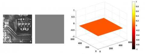
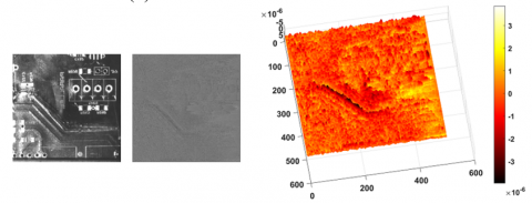
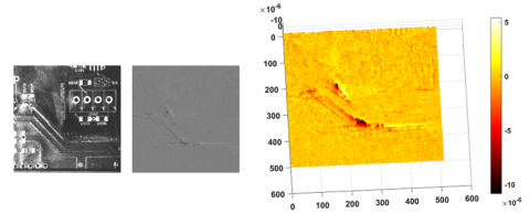
The holographic image is the pattern obtained by locating the sample PCB into the holographic recording medium created with LSDHM. The 2D wrapped phase image is the image in which information is reconstructed from the recorded holograms with signal processing algorithms. However, it is not possible to numerically given the extent of the distortion occurring in the PCB path due to the phase discontinuity in these images. For this reason, phase is unwrapped to make the phase values continuous and to show the numerical distortion amount in 3D. As a result of this process, 3D unwrapped phase images are obtained. In this context, the image obtained 0.02 seconds after applying 13.5 A to path I is presented in Figure 7a. With HOIS, 50 frames per second (hologram) are recorded. The image taken at 0.02 s belongs to the first captured hologram. Figure 7b shows the image obtained 0.02 s after applying 11.5 A to path III. According to these figures, it is understood that even if different currents are applied in two identical paths at 0.02 s, no swelling occurs. In addition, when comparing the reference holograms presented in Figure 6 with the recorded hologram images at this time (0.02 s), it is impossible to see this difference with the naked eye. Despite it not being noticeable by the naked eye from the recorded holograms in Figure 7c and Figure 7d, it is very clearly seen that swelling begins in 1.1 s on the path I applied at 13.5 A in both the reconstructed 2D wrapped and the 3D unwrapped phase images. On the other hand, it can be said that while there is no deterioration at 1.1s on the path III, which is applied 11.5A, it starts at 1.3 s. (See Figure 7e). The captured image at 1.1 seconds is the 55th hologram and the recorded image at 1.3 seconds is the 65th hologram.
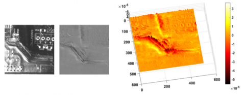
Although the deterioration (swelling) on the path cannot be seen clearly with the naked eye, the amount of swell on the paths increases as the current continues to be applied to the determined path. However, the size of this swell varies according to the amount of current supplied to the path. This is clearly seen in Figure 8a and Figure 8b. With a current of 13.5 A applied to the path I, a swelling almost as long as the path occurred in the 4th s (See Figure 8a). On the other hand, the swelled path length in the path III, where 11.5 A is applied in the same second (4 s), is shorter. (See Figure 8b).
As long as the determined currents continue to be supplied to the relevant paths, the swelling on the paths reaches a visible level. However, depending on the increasing temperature, it can be seen that smoke comes out of the relevant paths while examining. In Figure 8c, it is seen that there is a smoke outlet directed upwards like a line at 14.12 s in the path I, where a current of 13.5 A is applied. At the same time, deterioration (faults) on the path can be seen directly not only from the 2D and 3D phase images, but also from the recorded hologram. On the other hand, while no smoke is observed at 14.12 s on the path III (See Figure 8d), it can be said that there is a visible smoke and deterioration at 76.16s. (See Figure 8e).
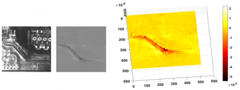
The clearest visible distortion (swelling) in all of the paths occurs at 26.6s in the path I, while it occurs at 282.4 s in the path III. In Figure 9a and Figure 9b, the deterioration patterns occurring in the I and III pathways are shown at the specified times. As it can be understood from this, it can be said that when two different currents are applied to two paths with the same characteristic path structure, the occurrence times of invisible and visible swellings are quite different. As the amount of current applied increases, the distortion time of the path becomes faster.
a. Path I with 13.5 A at 4 s
b. Path III with 11.5 A at 4 s
c. Path I with 13.5 A at 14.12 s
d. Path III with 11.5 A at 14.12 s
e. Path III with 11.5 A at 76.16 s
Figure 8. The holograms and their related 2D wrapped and 3D unwrapped phase images for path I and path III at 4s, 14.12s and 76.16 s
a. Path I with 13.5 A at 26.6 s
b. Path III with 11.5 A at 282.4 s
Figure 9. The holograms and their related 2D wrapped and 3D unwrapped phase images for path I and path III at 26.6s and 282.4s
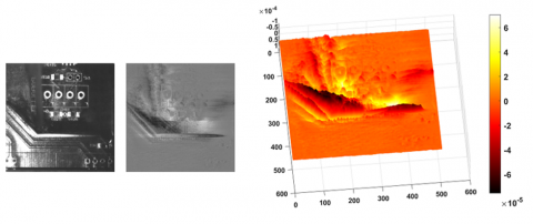
In order to strengthen the accuracy of the results in the study, a current varying between 8A and 13.5A is applied to Path II instead of applying a constant current. Obtained results are depicted in Figure 10. At this stage, 8A is applied to Path II for 65s. As in Path I and Path III, no deterioration occurred in this path for 0.02 s. The obtained results are shown in Figure 8a. However, while the deterioration occurred in 1.1 s and 1.3s at 13.5 A and 11.5 A applied to the other paths, respectively, the deterioration started to occur in 4 s in the II road with 8 A applied. (See Figure 10b). According to these results, it can be clearly seen that the initial occurrence time of the short-circuits fault increases as the amount of current decreases. Although the deterioration in this path started in 4 seconds, the amount of deterioration in the determined path did not increase even though current was applied for 65 seconds. In other words, the swelling does not occur in the whole path, but in a certain part of it.
a. Path II with 8 A at 0.02 s
b. Path II with 8 A at 4 s
c. Path II with 11.5 A at 6 s (71 s in total)
d. Path II with 13.5 A at 3.34 s (138.34 s in total)
Figure 10. The holograms and their related 2D wrapped and 3D unwrapped phase images for path II at 0.02th s, 4s, 71s and 138.34s
11.5 A is applied to this path after 65 seconds to examine the extent of the distortion expected to change depending on the current. Looking at Figure 8d, although the amount of deterioration on the path increased in the 14.2th second when 11.5 A is applied, there has been no visible smoke output. However, looking at Figure 10c, it is determined that there has been smoke output 6 s (71s in total) after 11.5A is applied. This is because 8 A is initially applied to the PCB path and increases saturation.
11.5 A is applied to Path II for 60 s. However, no swelling in the whole path, which can be clearly seen with the naked eye, has occurred in this current. For this reason, 13.5 A is applied to this path last. Due to the increased saturation with 8 A and 11.5 A, which have been applied uninterruptedly before, the whole path is deteriorated in a very short time and the smoke output can be clearly seen. As can be shown in Figure 9a, the whole path I applied 13.5 A deteriorated in 26.6 seconds, while it was observed that the whole path deteriorated 3.34 s after applying 13.5 A to path II. (See Figure 10d). In other words, considering the durations of 8 A and 11.5 A application, short-circuit faults occurred visibly in 138.4 s in total.
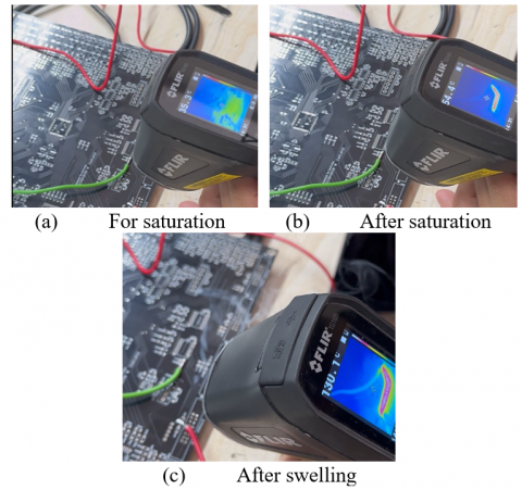
To prove the accuracy of the results in this study, the same experiments were carried out with a thermal camera (FLIR Extech-TG165), which is one of the traditional methods. For example, a constant 11.5 A was applied to path III.
Figure 11. The image obtained by using thermal camera
In order to detect faults with a thermal camera, it should first reach saturation at the specified temperature (expected to be at least 50℃). While the camera is saturating, no current is applied to the identified PCB path. In this study, the time taken to reach saturation is measured as 36 s. Figure 11 shows the image taken by the camera during the expected time for saturation. After the thermal camera reached saturation, 11.5A is applied to the PCB with a DC power supply. However, even though current is applied, the initial occurrence time of faults cannot be detected by using this camera. As seen in Figure 11b, only the path itself is visible in the image recorded at the 41st second after saturation. With a thermal camera, the SCF in the PCB path can be detected by the image taken when the swelling on the path becomes visible and smoke begins to appear. As seen in Figure 11c, a white smoke is observed in the environment as burning occurs on the path due to high current. Thermal camera temperature also shows 130℃.
When the results obtained with the thermal camera and the proposed HOIS are compared, it has been proven that SCF detection is made directly in the HOIS system without the need for saturation. Thus, the 36 s required for saturation of the thermal camera is eliminated. In addition, the IOT of SCF could be detected at 1.1 s with the HOIS, although it is not visible to the naked eye. However, since only visible faults (swelling) could be detected with the thermal camera, the first moment of formation of the SCF could not be imaged. On the other hand, the swelling on the path and the white smoke resulting from the burning of the path were recorded by HOIS at 76.16 s. In a thermal camera, this time is approximately 2 minutes. In fact, the purpose of using a thermal camera is not to directly display the faults. It shows whether there is a fault by measuring the high temperature that will occur due to high current. Therefore, it only detects visible swellings that occur due to high temperatures.
In addition to all these results it can be said that as the amount of current increases, the sooner deterioration is occurred. Thanks to proposed HOIS, it is clearly shown in Figures 7-10 that short-circuit path faults are detected at the earliest stage, regardless of which current is applied without the need for any saturation.
The usage of PCB and its mass production have an important place in the electronics industry. On the other hand, PCBs are difficult to recycle due to the diversity of material components and the difficulty of separation. For this reason, all faults that may occur before mass production should be detected at the earliest stage. In this context, if SCF are not detected at an early stage and the fault in the relevant area is not eliminated, all PCB and other components will be damaged scrapped. If the PCB surface or related PCB paths are exposed to high current, the current application can be stopped if the time of onset of damage caused by the current is detected. This way the faults can be repaired without damaging other parts. This will make a great financial contribution to the electronics industry as it will reduce the amount of PCB waste.
In this study, HOIS-based fault detection is proposed to diagnose the IOT of SCF on big-sized PCBs paths. The diagnosing process are performed by using a cost effective optical microscopic sensor with minimum optical components rather than costly thermal cameras. In order to diagnose the SCF at the earliest stage, holograms, which contain the information of deteriorations, are recorded with the proposed system simultaneously while applying current to the PCB path.
Compared to all previous faults detections systems (including thermal-based systems), the proposed HOIS-based systems can detect faults before the PCB is damaged; therefore, before the mass productions the faults are repaired and the process can be resumed. In this context, the HOIS-based system provides cost-effectiveness not only by providing simple and easy to implement fault detection system but also by preventing PCBs turning out to be an electronic waste. In other words, by determining the IOT of SCF for a quality PCB inspection before mass production, possible larger failures can be avoided. Hence, the efficiency of the mass production can be improved that can save large amount of PCBs and provide very high cost-effectiveness.
HOIS-based system is also superior to previous methods in terms of fault detection performance. The thermal-based systems (i.e., mostly used in the industry) can only detect visible faults that requires a saturation time (e.g., 36 seconds). However, the more current is applied the worsen fault is occurred. Therefore, during this saturation time the fault can turned out to be unrepairable. On the other hand, with the HOIS-based systems, we can capture IOT of SCF at the very early stage (e.g., 1.1 seconds). Therefore, the process can be stopped immediately and the whole PCB can be rescued from an irrevocably fault.
In future works, we aim to turn the set-up a compact design. We also envision that with a machine learning-based algorithm, we can make classification for IOT of all types of faults (e.g., components) for not only path faults.
[1] Zhang, Q., Liu, H. (2021). Multi-scale defect detection of printed circuit board based on feature pyramid network. In 2021 IEEE International Conference on Artificial Intelligence and Computer Applications (ICAICA), Dalian, China, pp. 911-914. https://doi.org/10.1109/ICAICA52286.2021.9498174
[2] Ling, Q., Isa, N.A.M. (2023). Printed circuit board defect detection methods based on image processing, machine learning and deep learning: A survey. IEEE Access, 11: 15921-15944. https://doi.org/10.1109/ACCESS.2023.3245093
[3] Chang, P.C., Chen, L.Y., Fan, C.Y. (2008). A case-based evolutionary model for defect classification of printed circuit board images. Journal of Intelligent Manufacturing, 19: 203-214. https://doi.org/10.1007/s10845-008-0074-8
[4] Hassanin, A.A.I.M., Abd El-Samie, F. E., El Banby, G. M. (2019). A real-time approach for automatic defect detection from PCBs based on surf features and morphological operations. Multimedia Tools and Applications, 78(24): 34437-34457. https://doi.org/10.1007/s11042-019-08097-9
[5] Tan, C.M., Chen, H.H., Wu, J.P., Sangwan, V., Tsai, K.Y., Huang, W.C. (2022). Root cause analysis of a printed circuit board (PCB) failure in a public transport communication system. Applied Sciences, 12(2): 640. https://doi.org/10.3390/ app12020640
[6] Ustabaş Kaya, G. (2023). Development of hybrid optical sensor based on deep learning to detect and classify the micro-size defects in printed circuit board. Measurement, 206: 112247. https://doi.org/10.1016/j.measurement.2022.112247
[7] Ibrahim, Z., Rahman Al-Attas, S.A. (2005). Wavelet-based printed circuit board inspection algorithm. Integrated Computer Aided Engineering, 12(2): 201-213. https://doi.org/10.3233/ICA-2005-12206
[8] Yang, Y., Kang H. (2023). An enhanced detection method of PCB defect based on improved YOLOv7. Electronics, 12(9): 2120. https://doi.org/10.3390/electronics12092120
[9] De Lorenzo, D.S. (2002). Thermal design of high-density server. IEEE Transactions on Components and Packaging Technologies, 25(4): 635-640. https://doi.org/10.1109/TCAPT.2002.807996
[10] Netsu, T., Taniguchi, M., Ishida, H., Yanada, T., Takagi, T. (2005) Thermal analysis of printed circuit board due to thermal stress by using thermography and holography. In 2005 IEEE Instrumentationand Measurement Technology Conference Proceedings, Ottawa, Ont., pp. 1965-1969. https://doi.org/10.1109/IMTC.2005.1604515
[11] Stubbs, D.M., Pulko, S.H.,Wilkinson, A.J. (2002). An investigation of the sensitivity of embedded passive component temperatures to PCB structure. In IEEE Transactions on Components and Packaging Technologies, 25(4): 701-707. https://doi.org/10.1109/TCAPT.2002.806175
[12] Moganti, M., Ercal, F., Dagli, C.H., Tsunekawa, S. (1996). Automatic PCB inspection algorithms: A survey. Computer Vision and Image Understanding, 63(2): 287-313. https://doi.org/10.1006/cviu.1996.0020
[13] Bagavathiappan, S., Lahiri, B.B., Saravanan, T., Philip, J., Jayakumar, T. (2013). Infrared thermography for condition monitoring - A review. Infrared Physics & Technology, 60: 35-55. https://doi.org/10.1016/j.infrared.2013.03.006
[14] Kim, S.Y., Kim, J.D., Kim, Y.S., Song, H.J., Park, C.Y. (2015). Resistance temperature detector sensor with a copper pattern on the printed circuit board. International Journal of Control and Automation, 8(8): 67-74. http://dx.doi.org/10.14257/ijca.2015.8.8.08
[15] Yan, D., Yang, Y., Hong, Y., Liang, T., Yao, Z., Chen, X., Xiong, J. (2018). Low-cost wireless temperature measurement: Design, manufacture, and testing of a PCB-based wireless passive temperature sensor. Sensors, 18(2): 532-546. https://doi.org/10.3390/s18020532
[16] Nerone, M., Valic, I., Zauli, M., Leonardi, A., Matteazzi, N., De Marchi, L. (2022). A wirelessly-powered embedded system for temperature measurements of a high performance electric motor rotor. In 2022 IEEE International Workshop on Metrology for Automotive (MetroAutomotive), Modena, Italy, pp. 6-11. https://doi.org/10.1109/MetroAutomotive54295.2022.9855040
[17] Yilmaz, B., Ba, A., Jasiuniene, E., Bui, H.K., Berthiau, G. (2020). Evaluation of bonding quality with advanced nondestructive testing (NDT) and data fusion. Sensors, 20(18): 5127. https://doi.org/10.3390/s20185127
[18] Wang, F., Yue, Z., Liu, J., Qi, H., Sun, W., Chen, M., Wang, Y., Yue, H. (2022). Quantitative imaging of printed circuit board (PCB) delamination defects using laser-induced ultrasound scanning imaging. Journal of Applied Physics, 131: 053101. https://doi.org/10.1063/5.0077766
[19] Gaal, M., Dohse, E., Bartusch, J., Köppe, E., Kreutzbruck, M., Hillger, W., Amos, J.M. (2014). Ultrasonic testing of adhesively bonded joints using air-coupled cellular polypropylene transducers. In ECNDT 2014-11th European Conference on Non-Destructive Testing (Proceedings), pp. 1-8.
[20] Zheng, C., Lu, H., Hu, H., Zhao, W., Yuan, Y., Xu, Y., Wang, Y., Hu. Y. (2023). Research on printed circuit board external open-circuit failure gas discharge tube under short-circuit failure. Electric Power Systems Research, 220: 109337. https://doi.org/10.1016/j.epsr.2023.109337
[21] Swiderski, W. (2003). Lock-in thermography to rapid evaluation of destruction area in composite materials used in military application. Proceedings of SPIE - The International Society for Optical Engineering, 5132: 506-517.
[22] Straube, H., Breitenstein, O. (2011). Infrared lock-in thermography through glass substrates. Solar Energy Materials and Solar Cells, 95(10): 2768-2771. https://doi.org/10.1016/j.solmat.2011.05.017
[23] Strakowska, M., Strzelecki, M., Wiecek, B. (2018). Thermal modelling and thermography measurements of thermoregulation effects in a skin tissue. In 14th Quantitative Infrared Thermography Conference, pp. 127-135.
[24] Georges, M., Vandenrijt, J.F., Thizy, C., Pedrini, G., Vollheim, B., Ion, L., Aldave, I.J., Rochet, J., Osten, W. (2014). Combined holography and thermography in a single sensor through image-plane holography at thermal infrared wavelengths. Optics Express, 22(21): 25517-25529. https://doi.org/10.1364/OE.22.025517
[25] Li, M., Yao, N., Liu, S., Li, S., Zhao, Y., Kong, S.G. (2021). Multisensor image fusion for automated detection of defects in printed circuit boards. IEEE Sensors Journal, 21(20): 23390-23399. https://doi.org/10.1109/JSEN.2021.3106057
[26] Cong, S., Shang, Z., Huang. Q. (2022). Detection for printed circuit boards (PCBs) delamination defects using optical/thermal fusion imaging technique. Infrared Physics & Technology, 127: 104399. https://doi.org/10.1016/j.infrared.2022.104399
[27] Wang, F., Zhou, Y., Zhang, X., Li, Z., Weng, J., Qiang, G., Chen, M., Wang, Y., Yue, H., Liu, J. (2023). Laser-induced thermography: An effective detection approach for multiple-type defects of printed circuit boards (PCBs) multilayer complex structure. Measurement, 206: 112307. https://doi.org/10.1016/j.measurement.2022.112307
[28] Alaoui, N.E.B., Tounsi, P., Boyer, A., Viard, A. (2019). Detecting PCB assembly defects using infrared thermal signatures. 2019 MIXDES - 26th International Conference "Mixed Design of Integrated Circuits and Systems", Rzeszow, Poland, pp. 345-349. https://doi.org/10.23919/MIXDES.2019.8787089
[29] Seo K.B., Kim B.M., Kim E.S. (2014). Digital holographic microscopy based on modi- fied lateral shearing interferometer for three-dimensional visual inspection of nanoscale defects on transparent objects. Nanoscale Research Letters, 9(1): 471. https://doi.org/10.1186/1556-276X-9-471
[30] Ustabas Kaya, G., Kocabas, S., Kartal, S., Kaya, H., Tekin , I.O., Tigli Aydin, R.S., Kutoglu, S.H. (2022). Detection of airborne nanoparticles with lateral shearing digital holographic microscopy. Optics and Lasers in Engineering, 151: 106934. https://doi.org/10.1016/j.optlaseng.2021.106934
[31] Hu, Y., Chen, Q., Feng, S., Zuo, C. (2020). Microscopic fringe projection profilometry: A review. Optics and Lasers in Engineering, 135: 106192. https://doi.org/10.1016/j.optlaseng.2020.106192
[32] Liu, C.Y., Yen, T.P., Chen, C.W. (2020). High-resolution three-dimensional surface imaging microscope based on digital fringe projection technique. Measurement Science Review, 20(3): 139-144. https://doi.org/10.2478/msr-2020-0016
[33] Hu, Y., Chen, Q., Tao, T., Li, H., Zuo, C. (2017). Absolute three-dimensional micro surface profile measurement based on a greenough-type stereomicroscope. Measurement Science and Technology, 28(4): 045004. https://doi.org/10.1088/1361-6501/aa5a2d
[34] Zhu, F., Liu, W., Shi, H., He, X. (2010). Accurate 3D measurement system and calibration for speckle projection method. Optics and Lasers in Engineering, 48(11): 1132-1139. https://doi.org/10.1016/j.optlaseng.2009.12.016
[35] Wang, Z., Nguyen, D.A., Barnes, J.C. (2010). Some practical considerations in fringe projection profilometry. Optics and Lasers in Engineering, 48(2): 218-225. https://doi.org/10.1016/j.optlaseng.2009.06.005
[36] Tulsiani, D. (2005). A fringe projection system for measurement of condensing fluid films in reduced gravity. Ph.D. thesis, Worcester Polytechnic Institute.
[37] Yaroslavsky, L. (2003). Digital Holography and Digital Image Processing: Principles, Methods, Algorithms. Springer Science & Business Media.
[38] Goldstein, G., Creath, K. (2015). Quantitative phase microscopy: Automated background leveling techniques and smart temporal phase unwrapping. Applied Optics, 54(16): 5175-5185. https://doi.org/10.1364/AO.54.005175
[39] CR600x2 Camera Users' Manual, https://optronis.com/wp-content/uploads/2017/02/Camera-manual-english-1830-SU-02-N.pdf.
[40] Schnars, U., Falldorf, C., Watson, J., Juptner, W. (2015). Digital Holography and Wavefront Sensing: Principles, Techniques and Applications. Second Ed. Springer Heidelberg.
[41] Han, J., Duan, C., Lu, Q., Jiang, H., Fan, X., Wen, P., Ju, Y. (2019). Improvement of the crushing effect of waste printed circuit boards by co-heating swelling with organic solvent. Journal of Cleaner Production, 214: 70-78. https://doi.org/10.1016/j.jclepro.2018.12.288
[42] Kang, K.D., Ilankoon, I.M.S.K., Chong, M.N., Wu, T.Y. (2023). Exfoliation of coarse printed circuit boards using dimethylacetamide: Production of copper concentrates. Minerals Engineering, 191(1): 107963. https://doi.org/10.1016/j.mineng.2022.107963