Ola Mostafa*![]() | Nehad A. Zidan
| Nehad A. Zidan![]() | Wael Abbas
| Wael Abbas![]() | Hanady Hussein Issa
| Hanady Hussein Issa![]() | Nihal Gamal | Mostafa Fedawy
| Nihal Gamal | Mostafa Fedawy![]()
© 2023 IIETA. This article is published by IIETA and is licensed under the CC BY 4.0 license (http://creativecommons.org/licenses/by/4.0/).
OPEN ACCESS
In response to the growing demand for renewable energy sources, particularly solar energy, extensive research is being conducted to explore new materials and technologies that can enhance the efficiency and reduce the cost of solar cells. Perovskite Solar Cells (PSCs), with their high efficiency, low production cost, and adjustable bandgap, have emerged as a potential alternative to traditional silicon-based solar cells. However, concerns have been raised regarding the environmental and public health impacts of the toxicity of lead-based perovskite materials. Thus, the development of lead-free PSCs has recently gained significant attention. This study provides a simulated analysis of lead-free PSCs, employing CH3NH3SnI3 as the absorber layer. The primary objectives of this research include the identification of optimal materials for Electron Transport Layers (ETLs) and Hole Transport Layers (HTLs) to enhance cell performance, as well as an investigation into the influence of thickness, doping concentration, and the profile of doping concentration on device performance. These objectives were fulfilled using a 1D-Solar Cell Capacitance Simulator. Results from the simulation reveal that PSCs utilizing SnO2 and CuSbS2 for ETL and HTL respectively, demonstrate a high power conversion efficiency of 29.47%. Key performance indicators such as open circuit voltage, short circuit current density, and Fill Factor were recorded at 1.0241 V, 33.76 mA/cm2, and 85.22%, respectively. These findings offer valuable insights for the future development of efficient and environmentally-friendly PSCs.
optimization, toxic-free perovskite, solar cell, lead-free
Solar energy is a rapidly growing renewable energy source that has the potential to be crucial in addressing the world's energy and climate problems. Solar cell technology is at the core of solar energy generation, and researchers worldwide are attempting to produce more efficient and cost-effective solar cells to expand solar energy adoption. The creation of lead-free perovskite solar cells is one potential area of study in solar cell technology. Perovskite solar cells (PSCs) are a newer form of solar cell that has gained popularity in recent years owing to its high efficiency and inexpensive cost. The usage of lead in the perovskite material, on the other hand, has prompted worries about the environmental and health effects of these solar cells [1]. Lead-free PSCs which provide the same high efficiency and cheap cost as lead-based PSCs but without the environmental and health dangers associated with lead, are a possible answer to these problems [2]. As a result, the creation of lead-free PSCs is a crucial area of research with the potential to significantly advance solar cell technology and, ultimately, encourage the acceptance of solar energy as a sustainable and renewable energy source. In this context, researchers and engineers are hard at work developing novel materials and designs for lead-free PSCs offers great efficacy and long-term stability [3].
The most often used component in solar cell technology, silicon, is utilized to create the first generation of solar cells. These cells are very efficient, long-lasting, and dependable. They are, however, costly to make and use a large amount of energy. They are also hefty and inflexible, making integration into certain applications problematic [4]. The efficiency ratings for monocrystalline silicon and polycrystalline silicon range from 15% to 25% and 14% to 17%, respectively [5]. CdTe, CIGS, and GaAs are materials that are used in second-generation solar cells, commonly referred to as thin-film solar cells. These cells are less costly to produce than first-generation cells, and they may be formed into flexible, lightweight modules [6]. However, they are less efficient than first-generation cells and have a shorter lifespan.
Regardless of these disadvantages, second-generation solar cells remain an essential technology in the field of renewable energy. They are especially beneficial in applications where cost and flexibility dominate efficiency, such as mobile devices. The GaAs technology shows (PCE) of 29.1% [7]. CdTe and CIGS technologies have excellent efficiency, 22.1%, and 23.35%, respectively [6-8]. Third-generation solar cells are built using a wide range of novel and developing materials, including Copper Zinc Tin Sulfide (CZTS), Dye-Sensitized Solar Cells (DSSCs), Perovskite Solar Cells (PSC), Organic Photo Voltaics (OPVs), and Quantum Dot Solar Cells (QDSC). These cells have the potential to be more efficient than first-generation and second-generation cells while also being less costly to generate. They are, however, still in the early phases of development and face stability and durability difficulties over time [9, 10].
Due to its high efficiency, cheap cost, and straightforward manufacturing procedure, PSCs have emerged as a possible substitute for conventional silicon-based solar cells. The PCE of perovskite-based solar devices has increased significantly over the past decade, from 3.13% [11] to 25.8% [12]. Nevertheless, the toxicity of lead, which is often employed in the manufacture of PSCs, poses a significant problem for their application. This has raised questions about the possible harm perovskite solar cells may have to the environment and human health. Researchers have been working on lead-free PSCs that employ substitute components like tin, germanium, or bismuth to solve this problem [13, 14]. In addition to eliminating the toxicity issues related to lead-based PSCs, these lead-free PSCs have shown remarkable promise for high efficiency and stability [15]. There are still certain issues that need to be resolved in the development of lead-free PSCs, despite the advancements achieved in this area. To ensure these cells' long-term functioning, one difficulty is to increase their stability and robustness. Optimizing the performance of lead-free PSCs to attain efficiencies that are on par with or greater than lead-based perovskite solar cells is another difficulty [16]. Perovskite solar cells might revolutionize the solar energy sector by providing a low-cost alternative to current silicon-based solar cells, therefore their potential advantages are substantial. Other potential uses for perovskite solar cells include wearable electronics and photovoltaics incorporated into buildings.
This study aims to examine how various electron transport layers (ETLs) and hole transport layers (HTLs) affect the performance of CH3NH3SnI3 solar cells, based on experimental data from the literature [17]. To achieve this goal, we compared the efficiency of solar cells made from various ETL and HTL materials using the capacitance-simulating SCAPS-1D program. We also determined the optimal CH3NH3SnI3 solar cell thicknesses and doping concentration for ETL and HTL materials. The influence of different absorber layer doping profiles was simulated. Furthermore, this article examines the effect of absorber layer defect density on the performance of lead-free perovskite solar cells. We measured the solar cells' efficiency (PCE), fill factor (FF), open-circuit voltage (Voc), and short-circuit current density (Jsc). Overall, our study aimed to identify the most effective combination of ETL and HTL materials for improving the performance of CH3NH3SnI3 solar cells.
Numerical simulation tools used in semiconductor device modelling, including solar cells, include SETFOS, SCAPS, SILVACO, COMSOL, and ATLAS. Each program has unique benefits and drawbacks that may make it better or worse suited for certain research. A one-dimensional simulation program noted for its speed and ease of use is called SETFOS. However, its capabilities are limited in terms of the kinds of simulations that can be run, and it may not be appropriate for devices with complex structural designs. Another popular 1-D simulation program for modelling solar cells is SCAPS [18]. It can simulate a variety of device topologies and materials and has a simple to use interface. For large-scale simulations, it may not be as quick as other programs and would need more computing power. Three-dimensional simulation software called SILVACO is renowned for its precision and adaptability. It contains an integrated process simulator for modelling the production of devices, and it can simulate a broad variety of device topologies and materials. But it could be harder to use and have a higher learning curve than other programs. A Multiphysics simulation program called COMSOL can simulate a variety of physical processes, such as mechanical, thermal, and electrical effects. It may be used to replicate intricate device architectures and materials because of its considerable flexibility. However, compared to other programs, it could be more costly. A popular program for simulating semiconductor devices is ATLAS, which can simulate a variety of device topologies and materials. It can mimic electrical, thermal, and optical impacts and includes an integrated process simulator. For large-scale simulations, it could be more difficult to utilize than other programs and need for greater computing power [18]. Based on these factors, SCAPS 1D seems to be the best option for modelling solar cells. It is developed for 1D device architectures, which are employed in thin-film solar cells. The program simulates the flow of charge carriers in the device using the numerical solution of Poisson's equation and the continuity equations for electrons and holes. Poisson's equation defines the device's electric field and potential distribution, which is based on charge carrier distribution and material parameters. The continuity equations characterize the device's electron and hole flow, including charge carrier recombination and transport. Researchers may study how doping concentration, material attributes, and device dimensions affect solar cell performance using the program. It can also simulate the device's optical characteristics, including light absorption and reflection. This helps researchers simulate solar cell efficiency under varied light intensities and wavelengths. Overall, SCAPS 1D helps researchers predict and analyze solar cell performance [18].
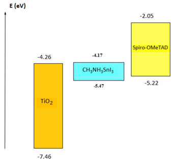
The experimental structure that is shown in Figure 1 was calibrated using SCAPS simulation. The structure composes of a glass base, TCO layer, ETL layer, an absorption layer made of perovskite, an HTL layer, and a back electrode. Each layer has a special function to help charge carriers move through the solar cell and convert the sunlight to electricity. The first layer from the bottom up is a glass base which gives the device mechanical support. The device's front electrode is a layer of transparent conductive oxide (TCO) that sits on top of the glass base. The TCO layer lets light go through the perovskite layer and provides a path for electrons to move along. The next layer is the buffer layer, which is also called ETL and is made of titanium dioxide ($\mathrm{TiO}_2$). The ETL layer moves electrons from the perovskite layer to the front electrode and stops holes from moving from the perovskite layer to the front electrode. The light-absorbing layer of the device is on the top of ETL layer. It is made of lead-free perovskite. Most of the time, methylammonium lead iodide $\left(\mathrm{MAPbI}_3\right)$ is used to make the perovskite layer. When light hits the perovskite layer, it creates electron-hole pairs, which are then divided by the electric field in the device and collected at the electrodes. HTL comes after the perovskite layer. It is made of Spiro-MeOTAD. The HTL layer facilitates the movement of holes from the perovskite layer to the back electrode while preventing the movement of electrons in the opposite direction. Lastly, the back electrode is a layer of metal that acts as the device's back contact and collects the holes that move through the HTL layer. Figure 2 shows the energy band diagram for the experimental materials. Table 1 lists the simulation inputs for layers. The J-V curve for the simulated structure at various defect density (Nt) levels is shown in Figure 3. The process of calibration indicated that our simulation model is well-aligned with the experimental observations. The observed structure's absorber layer's trap density was set to 5×1017 cm-3 to satisfy the J-V measurements obtained experimentally. To diminish the recombination rate and increase diffusion length, Nt must be reduced to enhance cell performance.
Figure 1. Simulated structure of PSC
Figure 2. Used experiment's materials energy band
Figure 3. Experimental J-V curves with variable Nt
Table 1. PSC device simulation parameters [19]
|
Parameters |
TCO |
TiO2 |
CH3NH3SnI3 |
Spiro-OmeTAD |
|
Thickness (nm) |
500 |
30 |
350 |
200 |
|
Bandgap (eV) |
3.5 |
3.2 |
1.3 |
3.17 |
|
Electron affinity χ (eV) |
4 |
4.26 |
4.17 |
2.05 |
|
Relative Dielectric permittivity (ԑr) |
9 |
9 |
8.2 |
3 |
|
CB effective density of states (cm -3) |
2.2×10¹⁸ |
2×10¹⁸ |
1×10¹⁸ |
2.2×10¹⁸ |
|
VB effective density of states (cm -3) |
1.8×10¹⁹ |
1.8×10¹⁹ |
1×10¹⁸ |
1.8×10¹⁹ |
|
Electron mobility µn (cm2/V. s) |
20 |
20 |
1.6 |
2×10⁻⁴ |
|
Hole mobility µp (cm2/V. s) |
10 |
10 |
1.6 |
2×10⁻⁴ |
|
Donor concentration ND (cm -3) |
2×10¹⁹ |
1×10¹⁶ |
0 |
0 |
|
Acceptor concentration NA (cm -3) |
0 |
0 |
3.2×10¹⁵ |
2×10¹⁹ |
|
Defect density Nt (cm -3) |
1×10¹⁵ |
1×10¹⁵ |
1016-1015 |
1×10¹⁵ |
|
Thermal velocities Vtht (cm/s) |
1×10⁷ |
1×10⁷ |
1×10⁷ |
1×10⁷ |
In this part, Electron Transport Materials (ETMs) and Hole Transport Materials (HTMs) were studied for the experimental device and optimised the thickness and doping of the ETL, the absorption layer, and HTL.
4.1 ETL optimization
ETL is optimized in this section. Various materials were utilized to choose the best suited ETM and identify its optimal thickness and doping. The defect kind being neutral, the electron capture cross section is 10-15 cm2, and the energy distribution is specified to be single for ETL density of defects of 1017 cm-3. The Donor concentration is set to be 1016 cm-3. Table 2 displays the input parameters for different ETMs. Furthermore, Figure 4 illustrates the energy band diagram for serval ETMs. Table 3 summarizes the device's performance for serval ETMs.
In PSCs, the consequences of the conduction band offset (CBO) between ETL and the perovskite layer (PL) have been researched. PSCs with varied conduction band energy levels in ETL were used to produce different attributes of CBO. The interface between PL and ETL affects the CBO values. The interface recombination mechanism takes over and the Voc lowers when the conduction band minimum (CBM) of the ETL is lower than that of the perovskite. When the CBM of the ETL is greater than that of the perovskite, interfacial recombination is greatly reduced, resulting in an enhancement of the solar cells Voc [20-22]. Due to that Voc in CdS reduces to 0.5601 V as negative CBO increases. SnO2 has been determined to be the most efficient ETL material for the PSCs based on the simulation results as obvious from Table 3. Since SnO2 has a high work function, it facilitates charge extraction and minimizes recombination losses at the perovskite/ETL interface, which is likely the cause.
Figure 4. Energy band diagrams for ETMs
Table 2. Parameters of input for various ETMs of the PSC structure
|
Parameters |
C60 [23] |
CdS [23] |
CdZnS [23] |
PCBM [23] |
SnO2 [20] |
$W s_2$ [23] |
ZnSe [21] |
STO [21] |
IGZO [23] |
ZNO [23] |
|
Thickness (nm) |
30 |
30 |
30 |
30 |
30 |
30 |
30 |
30 |
30 |
30 |
|
Bandgap (eV) |
1.7 |
2.4 |
3.2 |
2 |
3.5 |
1.8 |
2.81 |
3.2 |
3.05 |
3.3 |
|
Electron affinity χ (eV) |
3.9 |
4.5 |
4.2 |
3.9 |
4 |
3.95 |
4.09 |
4 |
4.16 |
4.1 |
|
Relative Dielectric permittivity (ԑr) |
4.2 |
10 |
9.120 |
3.9 |
9 |
13.6 |
8.6 |
8.7 |
10 |
9 |
|
CB effective density (cm -3) |
8×10¹⁹ |
2.2×10¹⁸ |
1.5×10¹⁸ |
2.5×10²¹ |
2.2×10¹⁷ |
2.2×10¹⁸ |
2.2×10¹⁸ |
1.7×10¹⁹ |
5×10¹⁸ |
4×10¹⁸ |
|
VB effective density (cm -3) |
8×10¹⁹ |
1.9×10¹⁹ |
1.8×10¹⁹ |
2.5×10²¹ |
2.2×10¹⁶ |
1.9×10¹⁹ |
1.8×10¹⁸ |
2×10²⁰ |
5×10¹⁸ |
1×10¹⁹ |
|
Electron mobility µn (cm2/V. s) |
8×10⁻² |
3.5×10² |
2.5×10² |
2×10⁻¹ |
2×101 |
1×10² |
4×10² |
5.3×10³ |
1.5×101 |
1×10² |
|
Hole mobility µp (cm2/V. s) |
3.5×10⁻³ |
2.5×101 |
4×101 |
2×10⁻¹ |
1×101 |
1×10² |
1×10⁻¹ |
6.6×10² |
1×10⁻¹ |
2.5×101 |
(b) Eff-FF
Figure 5. Performance variations of solar cells with relation to ETL thickness
(a) J-V
(b) Eff-FF
Figure 6. Performance variations of solar cells with relation to ETL doping
4.1.1 Optimization of SnO2 thickness
The ETL should be as thin as possible, however practical limitations in manufacturing prevent it from being smaller than 30 nm. To determine the impact of thickness variation on cell performance, the following study presents. Figure 5 shows a range of ETL thicknesses from 10 to 100 nm.
The simulation results demonstrated that the PSCs efficiency increased with decreasing SnO2 ETL layer thickness. There are probably several causes behind this. First, a thinner ETL layer may result in higher photocurrents and improved device efficiency since charge carriers have a shorter distance to travel from the perovskite layer to the front electrode. Additionally, the device's fill factor and efficiency may benefit from a thinner ETL layer by decreasing its series resistance. Additionally, as the ETL thickness is reduced, both the interface's bulk and surface recombination rates diminish.
4.1.2 Impact of SnO2 doping concentration
Concerning the effect of SnO2 doping concentration, illustrating results show that raising the doping concentration of the $\mathrm{SnO}_2$ ETL layer can both enhance photocurrents and the overall efficiency of the device. This is likely because there are more electrons in the ETL layer, which makes it easier to remove and move charges. But raising the amount of doping can also cause more recombination losses in the device, which can lower open-circuit voltage and device efficiency. So, there may be an optimal concentration of doping that achieves a balance between the effects of better charge extraction and higher recombination losses. Figure 6 displays the results when the thickness of SnO2 is set at 30 nm. The data illustrate that increasing the concentration of $\mathrm{SnO}_2$ layer doping with ranges from $10^{16}$ to $10^{21} \mathrm{~cm}^{-3}$ has distinct impacts on the PV parameters: the value of $V_{o c}$ is almost constant. At the same time, $J_{s c}$ is increased from 28.9 $\mathrm{mA} / \mathrm{cm}^{-2}$ to $30.14 \mathrm{~mA} / \mathrm{cm}^{-2}$ as shown in Figure 6 (a). On the other hand, FF has increased from $71.34 \%$ to $73.47 \%$, and power conversion efficiency has improved from $17.05 \%$ to $18.33 \%$ as depicted in Figure 6(b).
Table 3. Performance of the device for various ETMs
|
ETM |
Efficiency |
Current |
FF |
$V_{o c}$ |
|
TIO2 |
14.66 |
28.17086 |
65.85 |
0.7905 |
|
ZNO |
16.32 |
28.53 |
69.15 |
0.8272 |
|
ZnSe |
16.36 |
28.405163 |
69.66 |
0.8268 |
|
WS2 |
15.74 |
26.67009 |
71.69 |
0.8232 |
|
STO |
16.67 |
28.655195 |
70.35 |
0.8268 |
|
SnO2 |
17.05 |
28.908018 |
71.34 |
0.8266 |
|
PCBM |
15.09 |
26.79987 |
68.23 |
0.825 |
|
IGZO |
15.77 |
28.350185 |
67.40 |
0.8252 |
|
CdZnS |
15.65 |
28.35511 |
67.03 |
0.8233 |
|
CdS |
9.45 |
26.7972 |
62.97 |
0.5601 |
|
C60 |
14.73 |
25.7517 |
69.48 |
0.8235 |
4.2 CH3NH3SnI3 as absorber layer
The absorber layer is an important component of a solar cell because it absorbs photons from sunlight and converts them into electrical energy. The absorber layer's material and physical properties are critical in defining the efficiency and performance of the solar cell. The important absorber layer factors that affect solar cell performance are thickness and doping concentration. The thickness of the absorber layer is an essential element that influences the quantity of sunlight that the material can absorb. Enhanced absorber layer thickness may result in enhanced photon absorption, but it can also result in increased carrier recombination and lower efficiency. The absorber layer's doping concentration may impact the electrical characteristics of the material, including carrier concentration and mobility. As a result, the doping concentration used may have a substantial influence on the performance of the solar cell. The effect of thickness and doping concentration of the absorber layer are studied in this section.
4.2.1 Thickness optimization
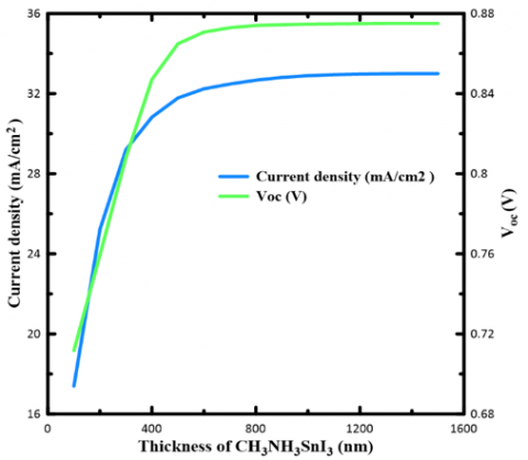
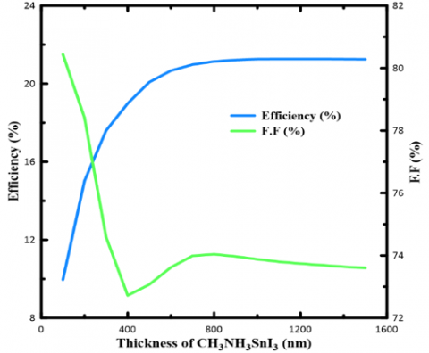
Since the absorber layer thickness significantly affects solar cell performance, it was expanded from 100 to 1,500 nm. As the thickness of the perovskite absorber layer is increased, the performance of the perovskite solar cell is observed to increase up to a specific point based on the simulation results. Several variables may have contributed to this. To begin, a thicker perovskite absorber layer can absorb lighter, which might increase photocurrents and the overall efficiency of the device. Beyond a certain thickness, however (in this situation, 1,000 nm), the device's performance levels out or even decline. This might be because of the device's higher series resistance, lower charge carrier extraction efficiency, or greater charge carrier recombination. Figure 7 depicts the results regarding the influence of absorber layer thickness on solar cell performance.
(a) J-V
(b) Eff-FF
Figure 7. Performance variations of solar cells with relation to absorber layer thickness
4.2.2 Impact of doping concentration of absorber layer
To begin, increasing the absorber layer's photocurrent requires increasing the density of charge carriers, which may be accomplished by doping. Doping could affect the perovskite material's energy levels and bandgap, which in turn can boost charge carrier transportation and lower recombination losses. However, if the doping concentration is raised above a certain point (in this example, $N_A$ equal to $10^{16} \mathrm{~cm}^{-3}$), the device's performance may begin to decline because of higher recombination losses and decreased charge carrier extraction. This is because an increase in doping concentration in a perovskite material may result in an increase in defects and trap states, which in turn can lead to an increase in non-radiative recombination and a decrease in the device's overall efficiency. As depicted in Figure 8, the effect of absorber layer doping is simulated for $N_A=10^{14} \mathrm{~cm}^{-3}$ to $N_A=10^{19} \mathrm{~cm}^{-3}$. According to the results of the study, doping may enhance PSC performance until it achieves a value of NA equal to $10^{16} \mathrm{~cm}^{-3}$, with $V_{o c}$ equal to $0.9031 \mathrm{~V}, J_{s c}$ equal to 31.82 $\mathrm{mA} / \mathrm{cm}^2, \mathrm{FF}$ equal to $74.13 \%$, and PCE equal to $21.3 \%$.
(a) J-V
(b) Eff-FF
Figure 8. Variation in solar cell performance cells with relation to absorber layer doping
4.3 HTL optimization
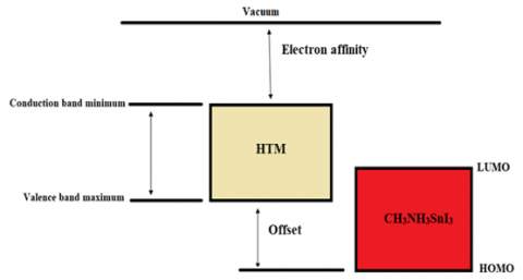
HTM layer is utilized to transport holes from the perovskite absorber layer. Concurrently it restricts backflow from the perovskite to the HTM. Table 4 presents the input parameters for several HTMs. In this part, the conduction band offset affects cell function is studied. Figure 9 depicts a schematic illustration of the position of the band offset at the intersection of the HTM.
When the valence band offset (VBO) has a positive value, the maximum of the HTM layer's valence band is lower than that of the perovskite layer's HOMO layer. Large potential barriers arise between the two layers as the offset potential rises. This indicates that the holes formed in the perovskite layer have difficulty entering the HTM layer. It can also be shown that as the offset increases, the short-circuit current and open-circuit voltage remain practically the same [24]. On the other hand, when the Valance Band Offset is negative, the HTM layer valence band is higher than the perovskite layer. The outcomes show that even when the offset potential changes, the short-circuit current doesn't. However, the negative offset voltage increases as the open circuit voltage lower. The cell efficiency is reduced by raising the offset potential [20]. The device's performance for numerous ETMs is listed in Table 5.
Table 4. Input parameters for different HTMs of the PSC structure
|
Parameters |
CuI [25] |
NiO [21] |
MoO3 [23] |
CuSbS2 [25] |
SrCu2O2 [25] |
|
Thickness (nm) |
30 |
30 |
30 |
30 |
30 |
|
Bandgap (eV) |
2.98 |
3.8 |
3 |
1.58 |
3.3 |
|
Electron affinity χ (eV) |
2.1 |
1.46 |
2.5 |
4.2 |
2.2 |
|
Relative Dielectric permittivity (ԑr) |
6.5 |
10.7 |
12.5 |
14.6 |
9.77 |
|
CB effective density (cm-3) |
2.8×10¹⁹ |
2.8×10¹⁹ |
2.2×10¹⁸ |
2.2×10¹⁸ |
2×10²⁰ |
|
VB effective density (cm-3) |
2×10¹⁹ |
1×10¹⁹ |
1.8×10¹⁹ |
2.2×10¹⁹ |
2×10²¹ |
|
Electron mobility µn (cm2/V. s) |
100 |
12 |
25 |
49 |
0.1 |
|
Hole mobility µp (cm2/V. s) |
43.9 |
2.8 |
100 |
49 |
0.46 |
Table 5. Performance of the device for various HTMs
|
HTM |
VBO |
Efficiency |
Current |
FF |
$V_{o c}$ |
|
Spiro-OmeTAD |
-0.25 |
18.13 |
31.551804 |
64.00 |
0.8979 |
|
NiO |
-0.21 |
20.45 |
31.744230 |
71.53 |
0.9005 |
|
CuSCN |
-0.17 |
21.28 |
31.813520 |
74.07 |
0.9031 |
|
$\mathrm{SrCu}_2 \mathrm{O}_2$ |
0.03 |
21.32 |
31.818955 |
74.19 |
0.9031 |
|
$\mathrm{MoO}_3$ |
0.03 |
21.39 |
31.840375 |
74.37 |
0.9032 |
|
$\mathrm{CuSbS}_2$ |
0.31 |
21.40 |
31.874383 |
74.34 |
0.9032 |
Figure 9. A schematic illustration of the valence band offset at the junction of the HTM layer and perovskite
$\mathrm{CuSbS}_2$ has been determined to be the most effective HTL material among all the materials examined in this investigation with PCE=21.40 %. The selection of HTL material is crucial in determining the performance of PSCs, as it plays a crucial role in extracting and transporting the positive charge carriers (holes) produced in the absorbent layer towards the electrode. $\mathrm{CuSbS}_2$ 's advantageous energy band alignment with the CH3NH3SnI3 absorber layer may have contributed to its superior performance as an HTL material in this investigation. The $\mathrm{CuSbS}_2$ conduction band minimum (CBM) is well aligned with the CH3NH3SnI3 valence band maximum (VBM), which enables efficient hole transport and collection in the device.
4.3.1 Thickness optimization of HTL
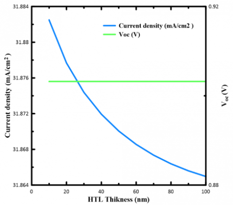
Results from the study indicate that adjusting the HTL thickness of a PSC does not significantly alter the device's efficiency as shown in Figure 10. $\mathrm{CuSbS}_2$ from 10 nm to 100 nm. Expanding the HTL thickness raises the series resistance, whereas decreasing its thickness decreases shunt resistance and current leakage, resulting in a lower recombination chance at interface between HTL, perovskite absorber layer [26] and comparatively high mobility of holes in the HTL layer.
(a) J-V
(b) Eff-FF
Figure 10. Performance of solar cells with relation to HTL thickness
4.3.2 The effect of HTL doping concentration
Additional acceptor states introduced by doping the HTL from $N_A=1 * 10^{14} / \mathrm{cm}^3$ to $N_A=1 * 10^{20} / \mathrm{cm}^3$. It may improve hole transport and lower recombination losses. More doping may not significantly improve the device's performance, however, when a specific threshold has been reached (in this example, $N_A=1 * 10^{19} / \mathrm{cm}^3$). In general, the research found that $V_{o c}$ and $J_{s c}$ of the device were unaffected by the acceptor doping of the HTL as illustrated in Figure 11 (a). This is probably because the energy levels and bandgap of the HTL material, the two fundamental parameters influencing $V_{o c}$ and $J_{s c}$, are not drastically changed by the acceptor doping. However, the findings of the research indicate that acceptor doping may have a major effect on the FF and overall device efficiency as shown in Figure 11 (b). The enhanced charge transport and decreased recombination losses in the HTL layer are likely responsible for this phenomenon, which may boost the device's charge collecting efficiency and lower its series resistance. When acceptor doping levels are equivalent to $1 * 10^{19} / \mathrm{cm}^3$, a high efficiency of 21.42% is achieved with $V_{o c}, J_{s c}$, and FF of 0.9032V, 31.89 $\mathrm{mA} / \mathrm{cm}^2$, and 74.34, correspondingly.
(a) J-V
(b) Eff-FF
Figure 11. Performance of solar cells with relation to HTL doping
4.4 Impact of doping concentration profile of absorber layer
Different doping profiles of perovskite absorber layer were simulated. The doping was $10^{20} 1 / \mathrm{cm}^3$ at the left side of the layer and $10^{16} 1 / \mathrm{cm}^3$ at the right-side layer. The output parameters of Linear doping, Gauss doping and Erfc doping are illustrated in Figure 12. It can be indicated from the Figure that Gauss and Erfc doping almost has the same output.
Figure 12. Solar cells performance in different doping types of absorber layer
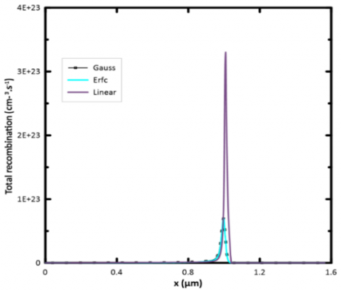
The recombination rate for different doping levels is plotted in Figure 13 to understand the impact of different doping profiles of the perovskite absorber layer on the performance parameters.
According to the recombination rate's performance, Gauss and Erfc doping are advantageous for reducing recombination because they improve carrier separation and boost the PCE of PSC by increasing photo absorption, which is caused by a rise in the electric field.
Furthermore, Table 6 shows the designed lead-free PSC performance in various values of absorber layer trap density. The proposed structure has an efficiency up to 29.47%.
Figure 13. Recombination rate vs distance for different doping profiles
Table 6. Optimized PSC performance
|
Nt(cm-3) |
Voc(V) |
Jsc(mA/cm2) |
FF % |
PCE % |
|
1×10¹⁶ |
0.9527 |
31.278133 |
79.96 |
23.83 |
|
1×10¹⁵ |
1.0241 |
33.762809 |
85.22 |
29.47 |
The primary elements impacting PSCs' efficiency are the perovskite material, the ETM, and the HTM. Additionally, the PSC layers' thickness and doping concentration affect the cell performance. A comparative survey of several perovskite solar cells with the presented work from PCE point of view is presented in Table 7.
Table 7. PCE comparison study
|
Reference |
Device Structure |
PCE (%) |
|
[27] |
$\mathrm{FTO} / \mathrm{SnO}_2 / \mathrm{MAPbI}_3 / \mathrm{CuSCN}$ |
26.74 |
|
[28] |
$\mathrm{FTO} / \mathrm{TiO}_2 / \mathrm{CH}_3 \mathrm{NH}_3 \mathrm{SnI}_3 / \mathrm{Cu}_2 \mathrm{O}$ |
27.43 |
|
[29] |
$\mathrm{FTO} / \mathrm{PCBM} / \mathrm{CH}_3 \mathrm{NH}_3 \mathrm{SnI}_3 / \mathrm{CuI}$ |
25.05 |
|
[30] |
$\mathrm{FTO} / \mathrm{TiO}_2 / \mathrm{CH}_3 \mathrm{NH}_3 \mathrm{SnI}_3 / \mathrm{CZTS}$ |
20.28 |
|
[31] |
$\mathrm{FTO} / \mathrm{TiO}_2 / \mathrm{CH}_3 \mathrm{NH}_3 \mathrm{GeI}_3 /$ Spiro-OMeTAD |
23.56 |
|
[32] |
$\begin{gathered}\mathrm{FTO} / \mathrm{TiO}_2 / \mathrm{CH}_3 \mathrm{NH}_3 \mathrm{SnI}_3 / \text { Spiro- } \text { OMeTAD }\end{gathered}$ |
22.21 |
|
[33] |
$\mathrm{FTO} / \mathrm{PCBM} / \mathrm{FAPbI}_3 / \mathrm{SrCu}_2 \mathrm{O}_2$ |
26.48 |
|
[34] |
$\mathrm{ITO} / \mathrm{TiO}_2 / \mathrm{CH}_3 \mathrm{NH}_3 \mathrm{SnI}_3 / \mathrm{CuI}$ |
28.3 |
|
This work |
$\mathrm{TCO} / \mathrm{SnO}_2 / \mathrm{CH}_3 \mathrm{NH}_3 \mathrm{SnI}_3 / \mathrm{CuSbS}_2$ |
29.47 |
Table 7 shows that the proposed structure with the optimized thickness for ETL, HTL and absorber layres provides a higher efficiency.
Due to their high efficiency, low cost, and potential for extensive commercialization, perovskite solar cells have attracted a lot of attention recently. However, many of the components used in conventional PSCs, such lead, are hazardous to the environment and human health. Therefore, it is crucial to create environmentally friendly, lead-free PSCs. This study presents a simulated analysis of lead-free PSCs using $\mathrm{CH}_3 \mathrm{NH}_3 \mathrm{SnI}_3$ as the absorber layer. 1D-SCAPS was utilized for the simulation. The use of $\mathrm{SnO}_2$ as an ETL and $\mathrm{CuSbS}_2$ as an HTL have been shown to improve the performance of $\mathrm{CH}_3 \mathrm{NH}_3 \mathrm{SnI}_3$-based PSCs. The proposed lead-free PSC is a promising development for the field of eco-friendly solar cells, as it offers a potential alternative to traditional PSCs that contain toxic materials. Furthermore, the optimization of the layers thickness and doping concentration can further enhance the performance of the proposed PSCs. The thickness and doping concentration of ETL, absorber layer and HTL of the proposed solar cell were studied for wide ranges to get the best performance. The results show that a 30 nm ETL thickness with a $10^{20} \mathrm{~cm}^{-3} \mathrm{SnO}_2$ doping concentration was the optimal values. For the absorber layer the doping concentration and thickness were $10^{16} \mathrm{~cm}^{-3}$ and 1000 nm, respectively. The HTL thickness was 40 nm with $\mathrm{CuSbS}_2$ doping concentration $10^{19} \mathrm{~cm}^{-3}$. The proposed structure with the optimal thicknesses and doping concentrations were simulated. The efficiency of 21.42% has been attained, with corresponding values of $V_{o c}, J_{s c}$ , and fill factor of 0.9032V, 31.89 $\mathrm{mA} / \mathrm{cm}^2$, and 74.34, respectively.
The impact of various absorber layer doping profiles was simulated to get higher efficiency. The simulation results evident that the Gauss doping enhances the performance of the proposed PSC.
Furthermore, this study investigates the effect of absorber layer defect density on the efficacy of lead-free perovskite solar cells. The investigation specifically considered two different values of $N_t$. The PCE of the optimized PSC were 23.83% and 29.47% at $N_t=10^{16} \mathrm{~cm}^{-3}$ and $N_t=10^{15} \mathrm{~cm}^{-3}$, respectively.
For comparable device structures, previous studies have reported efficiencies ranging from 15 to 28 percent. The proposed PSC achieved a higher efficiency comparing with the similar reported PSC by 3.9%.
Future research in the field of lead-free PSC has a lot of promise since it is still in its early phases. Alternative materials might be used as the absorber layer in PSCs, which could be a focus of future study. $\mathrm{Cs}_3 \mathrm{Bi}_2 \mathrm{I}_9$ and $\mathrm{Cs}_2 \mathrm{AgBiBr}_6$ are two interesting compounds now under investigation. Researchers will need to investigate a range of ETLs and HTLs that might be utilized in conjunction with these absorber materials to further increase the PCE of cells based on these materials. There are several materials that might be utilized as ETLs and HTLs in lead-free PSCs, and determining the best combination of materials will be a major focus of future research.
Overall, the results of this study have important implications for the development of eco-friendly solar cells. The use of lead-free materials and the optimization of device structures can lead to the production of low-cost, high-efficiency PSCs that are environmentally friendly and safe for human health.
[1] Bag, A., Radhakrishnan, R., Nekovei, R., Jeyakumar, R. (2020). Effect of absorber layer, hole transport layer thicknesses, and its doping density on the performance of perovskite solar cells by device simulation. Solar Energy, 196: 177-182. https://doi.org/10.1016/j.solener.2019.12.014
[2] Noel, N.K., Stranks, S.D., Abate, A., et al. (2014). Lead-free organic-inorganic tin halide perovskites for photovoltaic applications. Energy & Environmental Science, 7(9): 3061-3068. https://doi.org/10.1039/C4EE01076K
[3] McVeigh, J.C. (2013). Sun power: An introduction to the applications of solar energy. Elsevier.
[4] Fell, A., Schön, J., Schubert, M.C., Glunz, S.W. (2017). The concept of skins for silicon solar cell modeling. Solar Energy Materials and Solar Cells, 173: 128-133. https://doi.org/10.1016/j.solmat.2017.05.012
[5] Pastuszak, J., Węgierek, P. (2022). Photovoltaic cell generations and current research directions for their development. Materials, 15(16): 5542. https://doi.org/10.3390/ma15165542
[6] Roy, P., Ghosh, A., Barclay, F., Khare, A., Cuce, E. (2022). Perovskite solar cells: A review of the recent advances. Coatings, 12(8): 1089. https://doi.org/10.3390/coatings12081089
[7] Green, M., Dunlop, E., Hohl-Ebinger, J., Yoshita, M., Kopidakis, N., Hao, X. (2021). Solar cell efficiency tables (version 57). Progress in Photovoltaics: Research and Applications, 29(1): 3-15. https://doi.org/10.1002/pip.3371
[8] Nakamura, M., Yamaguchi, K., Kimoto, Y., Yasaki, Y., Kato, T., Sugimoto, H. (2019). Cd-free Cu (In, Ga) (Se, S) 2 thin-film solar cell with record efficiency of 23.35%. IEEE Journal of Photovoltaics, 9(6): 1863-1867. https://doi.org/10.1109/JPHOTOV.2019.2937218
[9] Płaczek-Popko, E. (2017). Top PV market solar cells 2016. Opto-Electronics Review, 25(2): 55-64. https://doi.org/10.1016/j.opelre.2017.03.002
[10] Noh, Y.W., Lee, J.H., Jin, I.S., Park, S.H., Jung, J.W. (2019). Enhanced efficiency and ambient stability of planar heterojunction perovskite solar cells by using organic-inorganic double layer electron transporting material. Electrochimica Acta, 294: 337-344. https://doi.org/10.1016/j.electacta.2018.10.138
[11] Kojima, A., Teshima, K., Shirai, Y., Miyasaka, T. (2009). Organometal halide perovskites as visible-light sensitizers for photovoltaic cells. Journal of the American Chemical Society, 131(17): 6050-6051. https://doi.org/10.1021/ja809598r
[12] Liu, Z., Liu, P., Li, M., He, T., Liu, T., Yu, L., Yuan, M. (2022). Efficient and stable fa-rich perovskite photovoltaics: From material properties to device optimization. Advanced Energy Materials, 12(18): 2200111. https://doi.org/10.1002/aenm.202200111
[13] Green, M.A., Hishikawa, Y., Dunlop, E.D., Levi, D.H., Hohl-Ebinger, J., Ho-Baillie, A.W.Y. (2018). Solar cell efficiency tables (version 52). Progress in Photovoltaics: Research and Applications, 26(7): 427-436. https://doi.org/10.1002/pip.3040
[14] Kumar, N.S., Naidu, K.C.B. (2021). A review on perovskite solar cells (PSCs), materials and applications. Journal of Materiomics, 7(5): 940-956. https://doi.org/10.1016/j.jmat.2021.04.002
[15] Tu, Y., Wu, J., Xu, G., et al. (2021). Perovskite solar cells for space applications: progress and challenges. Advanced Materials, 33(21): 2006545. https://doi.org/10.1002/adma.202006545
[16] Gamal, N., Sedky, S.H., Shaker, A., Fedawy, M. (2021). Design of lead-free perovskite solar cell using Zn1-Mg O as ETL: SCAPS device simulation. Optik, 242: 167306. https://doi.org/10.1016/j.ijleo.2021.167306
[17] Hao, F., Stoumpos, C.C., Cao, D.H., Chang, R.P.H., Kanatzidis, M.G. (2014). Lead-free solid-state organic-inorganic halide perovskite solar cells. Nature Photonics, 8(6): 489-494. https://doi.org/10.1038/nphoton.2014.82
[18] Pindolia, G., Shinde, S.M., Jha, P.K. (2022). Optimization of an inorganic lead free RbGeI3 based perovskite solar cell by SCAPS-1D simulation. Solar Energy, 236: 802-821. https://doi.org/10.1016/j.solener.2022.03.053
[19] Du, H.J., Wang, W.C., Zhu, J.Z. (2016). Device simulation of lead-free CH3NH3SnI3 perovskite solar cells with high efficiency. Chinese Physics B, 25(10): 108802. http/doi.org/10.1088/1674-1056/25/10/108802
[20] Ahmed, S., Jannat, F., Khan, M.A.K., Alim, M.A. (2021). Numerical development of eco-friendly Cs2TiBr6 based perovskite solar cell with all-inorganic charge transport materials via SCAPS-1D. Optik, 225: 165765. https://doi.org/10.1016/j.ijleo.2020.165765
[21] Singh, N., Agarwal, A., Agarwal, M. (2021). Performance evaluation of lead-free double-perovskite solar cell. Optical Materials, 114: 110964. https://doi.org/10.1016/j.optmat.2021.110964
[22] Ding, C., Zhang, Y., Liu, F., et al. (2018). Effect of the conduction band offset on interfacial recombination behavior of the planar perovskite solar cells. Nano Energy, 53: 17-26. https://doi.org/10.1016/j.nanoen.2018.08.031
[23] Bhavsar, K., Lapsiwala, P.B. (2021). Numerical simulation of perovskite solar cell with different material as electron transport layer using SCAPS-1D Software. Semicond. Semiconductor Physics, Quantum Electronics & Optoelectronics, 24: 341-347. https://doi.org/10.15407/spqeo24.03.341
[24] Jalalian, D., Ghadimi, A., Kiani Sarkaleh, A. (2020). Investigation of the effect of band offset and mobility of organic/inorganic HTM layers on the performance of Perovskite solar cells. Journal of Optoelectronical Nanostructures, 5(2): 65-78. https://jopn.marvdasht.iau.ir/article_4219.html.
[25] Karthick, S., Bouclé, J., Velumani, S. (2021). Effect of bismuth iodide (BiI3) interfacial layer with different HTL’s in FAPI based perovskite solar cell-SCAPS-1D study. Solar Energy, 218: 157-168. https://doi.org/10.1016/j.solener.2021.02.041
[26] Kim, G.W., Shinde, D.V., Park, T. (2015). Thickness of the hole transport layer in perovskite solar cells: Performance versus reproducibility. RSC Advances, 5(120): 99356-99360. https://doi.org/10.1039/C5RA18648J
[27] Raoui, Y., Ez-Zahraouy, H., Tahiri, N., El Bounagui, O., Ahmad, S., Kazim, S. (2019). Performance analysis of MAPbI3 based perovskite solar cells employing diverse charge selective contacts: Simulation study. Solar Energy, 193: 948-955. https://doi.org/10.1016/j.solener.2019.10.009
[28] Singh, A.K., Srivastava, S., Mahapatra, A., Baral, J.K., Pradhan, B. (2021). Performance optimization of lead free-MASnI3 based solar cell with 27% efficiency by numerical simulation. Optical Materials, 117: 111193. https://doi.org/10.1016/j.optmat.2021.111193
[29] Jayan, K.D., Sebastian, V. (2021). Comprehensive device modelling and performance analysis of MASnI3 based perovskite solar cells with diverse ETM, HTM and back metal contacts. Solar Energy, 217: 40-48. https://doi.org/10.1016/j.solener.2021.01.058
[30] Piñón Reyes, A.C., Ambrosio Lázaro, R.C., Monfil Leyva, K., et al. (2021). Study of a lead-free perovskite solar cell using CZTS as HTL to achieve a 20% PCE by SCAPS-1D simulation. Micromachines, 12(12): 1508. https://doi.org/10.3390/mi12121508
[31] Jan, S.T., Noman, M. (2022). Influence of layer thickness, defect density, doping concentration, interface defects, work function, working temperature and reflecting coating on lead-free perovskite solar cell. Solar Energy, 237: 29-43. https://doi.org/10.1016/j.solener.2022.03.069
[32] Tripathi, M., Mishra, V.V., Sengar, B.S., Ullas, A.V. (2022). Lead-free perovskite solar cell byUsing SCAPS-1D: design and simulation. Materials Today: Proceedings, 62: 4327-4331. https://doi.org/10.1016/J.MATPR.2022.04.832
[33] Noman, M., Shahzaib, M., Jan, S.T., Shah, S.N., Khan, A.D. (2023). 26.48% efficient and stable FAPbI 3 perovskite solar cells employing SrCu2O2 as hole transport layer. RSC Advances, 13(3): 1892-1905. https://doi.org/10.1039/D2RA06535E
[34] Noorasid, N.S., Arith, F., Mustafa, A.N., Chelvanathan, P., Hossain, M.I., Azam, M.A., Amin, N. (2023). Improved performance of lead-free Perovskite solar cell incorporated with TiO2 ETL and CuI HTL using SCAPs. Applied Physics A, 129(2): 132. https://doi.org/10.1007/s00339-022-06356-5