Saeed R. Saeed*![]() | Azad R. Kareem
| Azad R. Kareem![]() | Ashwaq Q. Hameed
| Ashwaq Q. Hameed![]()
© 2023 IIETA. This article is published by IIETA and is licensed under the CC BY 4.0 license (http://creativecommons.org/licenses/by/4.0/).
OPEN ACCESS
Cascaded Single-Stage Distributed Amplifiers (CSSDAs) are instrumental in achieving ultra-wideband amplification for microwave applications due to their significant gain-bandwidth products. However, their functionality is often compromised by internal noise, which detrimentally impacts the linearity of the response. An innovative solution to this prevalent issue is presented in this study through the introduction of the Quasi-Differential Distributed Amplifier (QDDA). Implementing the 0.18μm Complementary Metal Oxide Semiconductor (CMOS) technology, a QDDA with a single-stage four-cascade configuration was designed, fabricated, and tested. The empirical results revealed a high gain of 20dB and an extensive bandwidth of 30GHz. Moreover, the noise figure was observed to be 4.809 with a compact chip size of 0.74mm². This design and the resulting findings were accomplished using the Advanced Design System (ADS) RF simulator. The circuit layout and specifications were subsequently generated using the Cadence tool. This research demonstrates the potential of the QDDA to significantly enhance the performance of CSSDAs, contributing to the advancement of ultra-wideband microwave applications.
microwave amplifier, quasi-differential cascade distributed amplifier, differential amplifier gain bandwidth
Distributed amplification structure is used in many broadband applications such as microwave amplifiers [1], microwave oscillators [2], a microwave switches [3]. So, most wireless, mobile, satellite, optical, and radar systems need it [4-8]. Although the most important determinant of gain and bandwidth in microwave and RF amplifiers are transistor technology, and the product of gain in bandwidth (GBP) is constant, the physical environment of the transistors (design) affects and limits the practical gain and bandwidth of amplifiers [9]. The old design methods of broadband amplifiers such as compensator amplifiers, feedback amplifiers, and balanced amplifiers generally do not match the high GBP requirement, but the Distributed Amplifier (DA) is the most important microwave amplifier that can reach high values of GBP [10, 11]. The transmission cable limits the amplifier’s bandwidth of the gate and drain circuits, which is a major difficulty in DA theory [12]. High GBP can be attained using interest growth methods if the problem of bandwidth constraint can be overcome [13, 14]. Increasing the interest in each stage of a DA amplifier is undoubtedly the simplest approach to raise its appeal. The first conceivable solution for this is to enhance the transconductance [15]. However, raising gm requires either increasing the operating point current or increasing the transistor size, both of which result in additional constraints such as greater circuit power consumption and transistor capacitors, lowering the circuit’s bandwidth and thus not boosting GBP. As a result, this method has limited maneuverability, and to get high GBP, first designing high-bandwidth amplifiers and then multiplying the amplifiers is considered. A variety of layouts can benefit distributed amplifiers in their cell structure. Because of its capacity to reject common-mode voltages, one of the utility cells that can be used to increase the overall bandwidth of a distributed amplifier is the differential amplifier, making the circuit more immune to external noise [16]. However, because the differential amplifier has two inputs and outputs, to use it as a distributed amplifier gain cell, they need a balun for single-ended applications which limits the bandwidth [17]. This article aims to propose the Quasi Differential QD amplifier, which has a differential amplifier built with a single-ended input and single-ended output. It will give the amplifier two advantages, the first is to make use of differential amplifier features in having a high BW and low noise, the second is to eliminate the need for the balun circuit in which the proposed technique is a single-ended input and single-ended output and at the same time, it maintains the high BW obtained from the differential amplifier. The proposed QDA technique is adopted in the design of a cascaded single-stage distributed amplifier CSSDA, which is the best version of distributed amplifier in the matter of high gain and great GBP. CMOS technology is used to build microwave circuits because of its low cost. Many scholars proposed some improvement methods to remedy the defects in conventional distributed amplifiers. Beheshti et al. [18] propose a cascaded single-stage distributed amplifier-based broadband bandpass amplifier (CSSDA) approach using CMOS technology. The CMOS CSSDA’s normal low pass LC filter structure is substituted with bandpass LC filter structure lines in this configuration. In the passband, The CSSDA features a relatively constant gain and linear phase response, as well as a tolerable return loss. It has very good gain of 30dB but poor bandwidth of 11.5 GHz. Mogheyse and Miar Naimi [19] develop a novel approach for complete in distributed amplifiers with multiplicative gain stages, power combining is possible in this approach. In terminating resistors, power created by intermediary stages of multiplicative structures is always wasted. According to this research, an electrical funnel may be utilized to combine all of the created energy from all phases. The amplifier gains about 17dB in a bandwidth of 25.7GHz. Kang et al. [20] used a Samsung 65 nm CMOS technology to create two cascaded, single-stage, and two-stage distributed amplifiers (DA) (CSSDA). They’re designed in a cascade to give a broad bandwidth and high gain. The compact architecture is achieved by using an m-derived filter configuration. Its bandwidth reached 20Ghz with gain of 13dB. Wu et al. [21] present signal reuse as possible in the distributed amplifier via feedback transformers that are used to connect the cascaded gain stages. With a correct coupling coefficient (k) of the feedback transformer, the gain-bandwidth (GBW) product of DA can be enhanced by increasing the bandwidth to 33.5GHz, while retaining average gain of 12dB without increasing the power consumption. Odedeyi et al. [22] highlighted for ultra-wideband amplification, in terms of gain-bandwidth, Superior topologies include the single-stage distributed amplifier (SSDA) and its derivative multiplicative amplifier topologies (i.e., cascaded SSDA (C-SSDA) and matrix SSDA (M-SSDA). The world's first M-SSDA and SSDA MMIC have been announced as two new monolithic microwave integrated circuit (MMIC) amplifiers. With a 250 nm emitter width, the Indium Phosphide DHBT method is used in both amplifiers. Babaeinik et al. [23], present a unique distributed amplifier design approach based on a Pseudo differential amplifier to gain wider bandwidth. The amplifier cannot achieve good voltage gain, and the result was a gain of 9dB and bandwidth of 50GHz in 0.58mm2 CMOS chip area.
From the above, it is clear that the gain-bandwidth response is restricted in the distributed amplifiers, increasing the gain can be achieved for lower bandwidth, and vice versa. This work proposed a new design for the DA using a modified differential amplifier cell to improve the gain and the bandwidth in same amplifier circuit.
Distributed amplification, which involves dispersing the parasitic capacitance of amplifying transistors (Cgs and Cds) throughout input and output transmission lines, is a popular technique for designing broadband amplifiers with tens of gigahertz of bandwidth [24]. The most popular type of traditional DA amplifier with artificial transmission lines is shown in Figure 1. The inductors Lg and Ld are used to construct constant-k T-filter sections with the parasitic capacitances of the transistors and then reduce their effects and enhance the bandwidth. Many transistors are used in the circuit to boost its overall gain. The image impedance is used to terminate the amplifier's gate and drain lines [25]. The gm or gain block is an active circuit (transistors). They chose the FET unilateral model for simplicity in the design.
The corresponding circuit for the distributed amplifier’s gate and drain lines is shown in Figure 2. Since the T-sections are LPF with cutoff frequency of ωc, so the bandwidth of the amplifier is limited by ωc. The transistors are connected in parallel form between the two transmission lines, the overall gain at the output line equals to the summation of the gain in each transistor. The power gain and BW of the distributed amplifier can determine by Eq. (1) and Eq. (2) respectively [26].
$G=\frac{N^2 \,\, g_m^2 \,\, R_I\, R_o}{4}$ (1)
$\omega_C=\frac{2}{\sqrt{L C}}$ (2)
where, L=Lg=Ld, C=Cgs=Cds, N=number of stages, gm=transconductance of the transistors, and RI and RO=the input and output loads. For impedance matching, RI=RO and equal to 50Ω.
Figure 1. Conventional distributed amplifier with artificial lines
Figure 2. A DA equivalent circuit with discrete components (a) gate line and (b) drain line
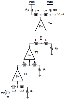
The cascaded single stage distributed amplifier or CSSDA is a modified distributed amplifier with N=1 that is built by cascading numerous single-stage amplifiers as depicted in Figure 3 [27]. It achieves a larger gain than a traditional distributed amplifier, where the gain is exponentially enhanced rather than being restricted solely by the square of the number of the stages [28]. This is particularly beneficial in CMOS technologies, where transconductance is often low [29].
Figure 3. CSSDA architecture
Figure 4. CSSDA equivalent circuit
The equivalent circuit of the CSSDA is shown in Figure 4. The T-filter sections are also found in the gate and drain lines of this circuit, so the bandwidth calculation, which depends on the L and C values, is not changed and the change will affect the gain calculation only.
In cascaded k-stages of CSSDA, the gain and bandwidth are calculated by the following equation [30]:
$G=\frac{g_m^{2 k} \,\,\, R_I^{2(k-1)} \,\,\,\,\, R_0^2}{4}$ (3)
$\omega_c=\frac{2}{\sqrt{L C}}$ (4)
As a comparison between Eq. (3) and Eq. (1), the DA's gain depends on ɡ2mwhile CSSDA's gain depends on ɡ2km, so for high gain CSSDA is used.
As a gain cell in distributed amplifiers, Quasi differential amplifier is proposed to be used because of the advantages of differential input, stable performance, noise cancellation, and good voltage gain. Figure 5 depicts a single stage of the QDDA amplifier. The current source in this circuit is transistor M3, whereas the bias transistors are M1and M2. The transistor's drain M2 collects the output, while M1 receives the input signal. Mc is a cascode transistor used to reduce the variation of the capacitance values in the gate and drain lines and then to obtain full bandwidth.
The equivalent circuit of the transistors in the Quasi differential amplifier configuration is shown in Figure 6.
The voltage gain of a QDA is identical to the gain of a conventional source amplifier and may be calculated as follows:
$\left|A_v\right|=\frac{1}{2} n g_m R_0$ (5)
The gate and drain lines of a Quasi differential distributed amplifier (QDDA) can be matched if their equivalent feature impedances are equal to the system impedance. In this case, the artificial transmission line is lossless and the cut-off frequency can be determined using the formula below:
$\omega_c=\frac{2}{\sqrt{L_g C_g}}=\frac{2}{\sqrt{L_d C_d}}=\frac{2}{z_0 C_0}$ (6)
Figure 5. Quasi differential distributed amplifier (QDDA) schema
Figure 6. Equivalent circuit of the Quasi differential amplifier
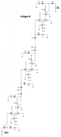
Figure 7. Schematic diagram of the proposed CSSQDDA
Cascading the DA is a common technique for achieving high gain to the DA amplifiers. In a typical DA, good input impedance matching and good input isolation give good stability and negligible harmonic factors and oscillation, and then good and easy cascading of the gain modules may be obtained. If k identical amplifier circuits are cascaded, the cascade gain will be as follows:
$\left|A_v\right|_{\text {cascade }}=\left|A_{\nu 1}\right|^k$ (7)
The voltage and power gains for cascaded single stage Quasi differential distributed amplifier (CSSQDDA) are:
$\left|A_v\right|_{\text {cascade }}=\left(\frac{1}{2} g_m R_0\right)^k$ (8)
$|G|_{\text {cascade }}=\left(\frac{1}{2} g_m R_0\right)^{2 k}$ (9)
The circuit shown in Figure 7 is the design of k-stages CSSQDDA. The cascade connection of multiple amplifier stages requires a blocking-dc section after each stage for dc isolations. It is a capacitor known as Metal-Insulator-Metal capacitor (MIM) [29].
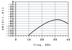
To validate the proposed idea of the CSSQDDA, it has been compared with the classical CSSDA. The two circuits used the same components for the passive and active cells and same number of stages (five) to gain 25dB for 30 GHz bandwidth. Figure 8 shows the simulation gain responses, the upper curve is the response of the proposed amplifier and the lower is the response of the classical amplifier.
Figure 8. Gain of CSSDA VS CSSQDDA
The CSSQDDA reaches more than 25dB gain and bandwidth of 30GHz as well as being stable and flat in the response, while CSSDA gives less gain and bandwidth about 20GHz. On the other hand, the CSSQDDA needs more transistors number.
Based on the benefits of the CSSQDDA, a proposed single-stage four cascades amplifier is designed. The goal is to achieve voltage gain S21=20dB, bandwidth=30GHz, reflection losses less than -10dB, and very low noise figure (NF). Using Eq. (6), the value of Lg and Ld are found corresponding to the values of Cg and Cd, while Eq. (8) used to find the necessary transconductance value. The obtained results of the circuit are given in Figure 9. It is performed by S-parameter analysis on ADS. The amplifier has an S21 of 20 dB and BW up to 30 GHz. Good reflection losses are also achieved. Figure 10 displays a Noise Factor (NF) of 4.809 dB as the lowest.
(a)
(b)
(c)
(d)
Figure 9. The S-parameter of proposed CSSQDDA (a) S21, (b) S11, (c) S22 and (d) S12
Figure 10. The NF of the proposed CSSQDDA
Table 1. A comparison of the previously announced distributed amplifiers as well as the completion of this work
|
References |
Gain (dB) |
BW (GHz) |
GBP |
NF (dB) |
Ripple (dB) |
Area mm2 |
Technology |
|
Ref [18] |
30 |
11.5 |
345 |
4.1 |
±2 |
2.02 |
0.13 μm CMOS |
|
Ref. [19] |
17.4 |
25.7 |
447 |
5.1 |
±2 |
_ |
0.18 μm CMOS |
|
Ref. [20] |
13 |
20 |
260 |
_ |
±1 |
0.39 |
65 nm CMOS |
|
Ref. [21] |
12 |
33.5 |
402 |
7 |
±2 |
0.72 |
0.18 μm CMOS |
|
Ref. [23] |
9 |
50 |
450 |
5.8 |
±2 |
0.58 |
0.18 μm CMOS |
|
This work |
20 |
30 |
600 |
4.809 |
±1 |
0.74 |
0.18 μm CMOS |
The final layout design of the amplifier is demonstrated in Figure 11. The implemented chip has a size of 813 mm×917 mm, or 0.74 mm2 when the pads are included. Off-chip capacitors and chokes are used in the bias circuit.
Figure 11. Micrograph of the proposed CSSQDDA
Table 1 presents a description for the performance of the proposed CSSQDDA and state-of-the-art CMOS CSSDA wideband amplifiers. As can be shown, proposed design has a high gain, good linearity, and an average NF when compared to previous studies. It is worth noting that if the same CMOS technology is employed, that is, if we take (or) into consideration, the benefits of the proposed (CSSQDDA) architecture will be more pronounced in areas where it achieves greater GBP as it is seen in the table where a GBP of 600 is obtained while the other works reaches 450 in max. The reason of this matter is in the use of differential amplifiers within the structure of the CSSQDDA which helps to eliminate undesired signals and keep flat response over the whole bandwidth, so wideband can be achieved, on the other hand, the gain of the proposed design is very high since it is exponentially depended on the number of stages.
The most important challenge in the design of the distributed amplifiers is the low gain-bandwidth product. Because of its great cut-off frequency, the Quasi-differential amplifier (QDA) topology was chosen for the DA design. This Means increasing the bandwidth by using differential amplifier cells instead of increasing the number of stages. A single-stage four cascaded (CSSQDDA) is built and tested in 0.18 µm CMOS technology with a successfully demonstrated wide bandwidth, high gain with high linearity. The measured results showed that the gain of the (CSSQDDA) is nearly matches the goal, while there is decay in the gain of the traditional CSSDAs, as well as higher bandwidth and better linearity. The achieved gain-bandwidth product could be regarded as one of the biggest gain-bandwidth products with better linearity. Thus, this circuit is useful in microwave applications. The suggested (CSSQDDA) occupies 0.74 mm2 layout area which is very acceptable in comparison to other works. The limitation which is hard to be exceeded is further increase in bandwidth because it is limited by the values of the parasitic elements in active and passive circuit. The low fabrication cost of CMOS made it widely used in microwave applications. In future works, other techniques instead of CMOS, for example, an InP can be used to enhance the bandwidth.
[1] Thome, F., Leuther, A. (2021). First demonstration of distributed amplifier MMICs with more than 300-GHz bandwidth. IEEE Journal of Solid-State Circuits, 56(9): 2647-2655. https://doi.org/10.1109/JSSC.2021.3052952
[2] Simion, S., Bartolucci, G. (2015). High power efficiency distributed oscillator based on composite-right-/left-handed unit cells. Applied Physics Letters, 107(10): 1-3. https://doi.org/10.1063/1.4930580
[3] Kareem, A.R. (2021). Advanced design for SPDT travelling wave switches. International Journal of Microwave & Optical Technology, 16(3): 261-267. https://doi.org/10.1109/LMWC.2021.3105578
[4] Jahanian, A., Heydari, P. (2012). A CMOS distributed amplifier with distributed active input balun using GBW and linearity enhancing techniques. IEEE Transactions on Microwave Theory and Techniques, 60(5): 1331-1341. https://doi.org/10.1109/TMTT.2012.2184134
[5] Zakerhaghighi, M.R., Mivehchy, M. (2016). A novel topology of distributed amplifier with low noise for radar application. Indian Journal of Science and Technology, 9(47): 1-6. https://doi.org/10.17485/ijst/2016/v9i47/101513
[6] Chen, Y., Xu, Y., Quan, J., Tong, W., Xu, R. (2018). A broadband GaAs high power millimeter wave amplifier with high gain and flatness. IEICE Electronics Express, 15(10): 20180229. https://doi.org/10.1587/elex.15.20180229
[7] Han, L., Wu, K. (2013). Joint wireless communication and radar sensing systems–state of the art and future prospects. IET Microwaves, Antennas & Propagation, 7(11): 876-885. https://doi.org/10.1049/iet-map.2012.0450
[8] Vasjanov, A., Barzdenas, V. (2020). 0.13 μm CMOS traveling-wave power amplifier with on-and off-chip gate-line termination. Electronics, 9(1): 133. https://doi.org/10.3390/electronics9010133
[9] Nguyen, N.L., Killeen, N.S., Nguyen, D.P., Stameroff, A.N., Pham, A.V. (2020). A wideband gain-enhancement technique for distributed amplifiers. IEEE Transactions on Microwave Theory and Techniques, 68(9): 3697-3708. https://doi.org/10.1109/TMTT.2020.3006165
[10] El Abdellaoui, L., Errkik, A., Tajmouati, A., Latrach, M. (2019). Design of a microstrip balanced amplifier using the Wilkinson power divider. Proceedings of the Third International Conference on Computing and Wireless Communication Systems, ICCWCS 2019, April 24-25, 2019, Morocco, pp. 96-105. http://doi.org/10.4108/eai.24-4-2019.2284098
[11] Mesgari, B., Saeedi, S., Jannesari, A. (2014). A wideband low noise distributed amplifier with active termination. 7’th International Symposium on Telecommunications, Iran, pp. 170-174. http://doi.org/10.1109/ISTEL.2014.7000691
[12] Virdee, G., Virdee, A.S., Banyamin, B.Y. (2004). Broadband Microwave Amplifiers, Artech House. Inc., Boston & London.
[13] Chen, P., Kao, J., Huang, P., Wang, H. (2011). A novel distributed amplifier with high gain, low noise, and high output power in 0.18-µm CMOS technology. 2011 IEEE MTT-S International Microwave Symposium. https://doi.org/10.1109/MWSYM.2011.5973318
[14] Alavi, S.A., Ghadirian, S., Chabok, S.J.S.M. (2017). Bandwidth and gain extension technique for CMOS distributed amplifiers using negative capacitance and resistance cell. Microelectronics Journal, 60: 60-64. https://doi.org/10.1016/j.mejo.2016.12.001
[15] Bhagavatula, V., Taghivand, M., Rudell, J.C. (2015). A compact 77% fractional bandwidth CMOS band-pass distributed amplifier with mirror-symmetric Norton transforms. IEEE Journal of Solid-State Circuits, 50(5): 1085-1093. https://doi.org/10.1109/JSSC.2015.2408322
[16] Hamada, H., Tsutsumi, T., Pander, A., Matsuzaki, H., Sugiyama, H., Takahashi, H., Nosaka, H. (2021). 220–325-GHz 25-dB-gain differential amplifier with high common-mode-rejection circuit in 60-nm InP-HEMT technology. IEEE Microwave and Wireless Components Letters, 31(6): 709-712. https://doi.org/10.1109/LMWC.2021.3061662
[17] Pandey, S., Gawande, T., Pathak, A., Kondekar, P.N. (2018). A 0.9-V, 4.4-mW CMOS LNA with wideband input match and high gain for UWB applications. International Journal of Electronics Letters, 6(3): 329-337. https://doi.org/10.1080/21681724.2017.1378373
[18] Beheshti, I., Uysal, S., Farokhiyan, F., Azar, F. (2012). Design of broadband bandpass cascaded single stage distributed amplifier in 0.13 μm CMOS technology for UWB applications. 2012 IEEE Symposium on Business, Engineering and Industrial Applications, Bandung, Indonesia, pp. 33-36. https://doi.org/10.1109/ISBEIA.2012.6422899
[19] Mogheyse, A.H., Miar Naimi, H. (2017). Two-dimensional distributed amplifier for extreme extension of GBW, PAE and OP1dB. IET Microwaves, Antennas & Propagation, 11(12): 1782-1790. https://doi.org/10.1049/iet-map.2016.1042
[20] Kang, S., Yunsik, N., Munkyo, S. (2017). Two-stage distributed amplifier and cascaded single-stage distributed amplifier in 65 nm CMOS process. Journal of Integrated Circuits and Systems, 3(2): 8-12. http://doi.org/10.23075/jicas.2017.3.2.002
[21] Wu, C.W., Huang, T.Y., Hsiao, Y.H., Wu, Y.C., Wang, H. (2017). A compact and low DC power distributed amplifier with cascaded gain stages using signal-reused technique in 0.18-pm CMOS. 2017 12th European Microwave Integrated Circuits Conference (EuMIC), Nuremberg, Germany, pp. 175-178. https://doi.org/10.23919/EuMIC.2017.8230688
[22] Odedeyi, T., Giannakopoulos, S., Zirath, H., Darwazeh, I. (2020). InP DHBT single-stage and multiplicative distributed amplifiers for ultra-wideband amplification. IEEE Transactions on Circuits and Systems I: Regular Papers, 67(11): 3804-3814. https://doi.org/10.1109/TCSI.2020.3025487
[23] Babaeinik, M., Dousti, M., Tavakoli, M.B. (2021). Analysis and design of high gain-bandwidth CMOS distributed amplifier utilizing a cascaded pseudo differential distributed amplifier. Journal of Circuits, Systems and Computers, 30(1): 2150005. https://doi.org/10.1142/S0218126621500055
[24] Song, S., Cen, M., Zhou, S. (2017). A 0.6 V 2.1–6.2 GHz low-power CMOS ultra-wideband low-noise amplifier for low-voltage operations. 2017 IEEE 17th International Conference on Communication Technology (ICCT), Chengdu, China, pp. 369-373. https://doi.org/10.1109/ICCT.2017.8359663
[25] Ho, P.H., Lin, Y.H., Wang, H., Meliani, C. (2014). A broadband 75 to 140 GHz amplifier in 0.13-µm SiGe HBT process. 2014 44th European Microwave Conference, Rome, Italy, pp. 1368-1371. https://doi.org/10.1109/EuMC.2014.6986699
[26] Alavi-Rad, H., Ziabakhsh, S., Yagoub, M.C. (2013). A 1.2 V CMOS common-gate low noise amplifier for UWB wireless communications. Journal of Circuits, Systems, and Computers, 22(7): 1350052. https://doi.org/10.1142/S0218126613500527
[27] Nikandish, G., Staszewski, R.B., Zhu, A. (2018). The (R) evolution of distributed amplifiers: From vacuum tubes to modern CMOS and GaN ICs. IEEE Microwave Magazine, 19(4): 66-83. https://doi.org/10.1109/MMM.2018.2813838
[28] Liang, J.Y., Aitchison, C.S. (1995). Gain performance of cascade of single-stage distributed amplifiers. Electronics Letters, 31(15): 1260-1261. https://doi.org/10.1049/el:19950828
[29] Shailesh, Srivastava, G., Kumar, S. (2021). A state-of-the art review on distributed amplifiers. Wireless Personal Communications, 117: 1471-1525. https://doi.org/10.1007/s11277-020-07932-9
[30] Eriksson, K., Darwazeh, I., Zirath, H. (2015). InP DHBT distributed amplifiers with up to 235-GHz bandwidth. IEEE Transactions on Microwave Theory and Techniques, 63(4): 1334-1341. https://doi.org/10.1109/TMTT.2015.2405916