Mehdi Ghoumazi
© 2023 IIETA. This article is published by IIETA and is licensed under the CC BY 4.0 license (http://creativecommons.org/licenses/by/4.0/).
OPEN ACCESS
The author of this article illustrates a new design and simulation of a twodimensional photonic crystal (PhC) based hydrostatic pressure sensor with a wide dynamic range that ranges from 0 to 4 Gpa and is conducted at a high resolution using the Finite Elements Method (F.E.M) under COMSOL software. In order to analyze the detection principle and its characteristics, the sensor is based on a triangular array PhC-2D of air-immersed silicon rods with a refractive index of 3.6 is used. The sensor consists of a hexagonal shaped ring resonator, which sits between two obtuse angle shaped waveguides. The two waveguides are configured by removing a row of B rods (line faults) and the ring resonator by removing a few rods. This ring resonator reduces the effect of external parameters such as humidity, temperature, etc. The band diagram is presented as well as analyzed using the plane wave expansion (PWE) under the Mat lab software on the one hand and on the other hand, on the other hand, results are obtained and illustrated such as: the distribution of the refractive index ‘n' within the structure with the mesh, the distribution of the electric field (TE) at resonance in 2 and 3D, the total energy density (TED), the power flow norm (PFN) and transmission. The sensor is designed for wavelengths between 1520nm and 1640nm.The simulation results show that due to the applied pressure, the refractive index of a sensor is changed and thus the resonant wavelength is shifted linearly to longer wavelengths.The designed sensor behaves linearly between 0GPa and 4GPa of applied pressure and 4.6 nm/GPa of pressure sensitivity.
photonic crystal, pressure sensor, finite element method, PWE method, detection
For many years, and among the known sensors used in industry, there are electrochemical sensors [1]. These sensors use a chemical reaction to measure the concentration of a specific gas in an environment [2]. They are present and exist in many different applications and continue to play a crucial role. Some of the most common applications are the detection of explosive gases and toxic vapors [3], food quality control [4], oxygen monitoring in the medical sector [5] and environmental monitoring of the air quality [6]. Today's need for small, low-power, and easy-to-use sensors has enabled the continued development of this technology. In addition, they can be built differently depending on the application, and therefore provide tailor-made solutions to new emerging applications. Additionally, they work by reacting with the targeted gas and producing an electrical signal proportional to its concentration. Composed of two electrodes (a working electrode and a counter-electrode), the sensor works by allowing charged molecules to pass through a thin layer of electrolyte. On the other hand, nowadays the most efficient sensors found on the market, whatever their type, use at least one resonator implanted in a photonic crystal structure [7]. These are the basis for the production of sensors for domestic use such as biological sensors [8], mechanical sensors [9], and chemical and/or gas sensors or for special purposes such as in the military or space fields [10-12]. To be able to "control" light as we "control" electrons in today's electronic devices, such a challenge seems a priori very difficult to meet! Yet this is the performance that photonic crystals can achieve.
A new work of research in the field of optical detection is explored by photonic crystals (Phcs) [13-14]. These Phcs are materials with spatially and periodically modulated refractive index. This periodicity is defined by a wavelength region (λ) in which the propagation of optical waves is prohibited. This wavelength region is called PBG which means photonic bandgap [15].The utility of PBG allows to confine the behavior of light on one side and control it inside Phcs in very small spaces on the other side [16], which represents one of the most important characteristics of the photonic crystal (Phc) from which it can be used in various detection applications such as: the detection of volatile organic compounds that can infect human health [17]. Moreover, in the wavelength interval (λ) of the PBG the light signal cannot propagate inside the structure as it can only be limited by introducing the defects of the perfect structure of the Phc. These defects are classified as point and line defects [18-19]. Basically, PhC platforms are classified into one, two and three dimensions, with the two-dimensional photonic crystal (PhC) being an important candidate for the development of photonic devices due to its: simple structure, small size, strong light confinement and the calculation of the perfect PBG_ as well as its ease of integration with photonic integrated circuits [20].Among the previous platforms is defined the sensor. The sensor is a device that can detect and respond to some different inputs from the physical environment [21].Optical sensors (OSs) are very important because of the advantage over electronic sensors. They can be designed using optical fiber [22, 23], photonic crystal fiber [24] and photonic crystals [25- 29].The search domains of PBG structures can be used for various applications. Their application as a sensor is a new area of research that seems to apply to nano electromechanical systems (NEMS) [30].In addition, within a few years, candidates such as optical sensors based on microstructures have become very promising and attractive for photonic integrated circuits, because they meet the current demand for lightness, ultra-compact size, their high sensitivity, their immunity to electromagnetic interference, from their rapid response speed to low power and precise detection of different substances [31].These candidates have been effectively used in wide range applications to detect various parameters such as: bio-analytes [32], electric fields [33], glucose concentration [34], cancer cells [35], seawater salinity [36], blood components [37], chemical gas [38], DNA molecules [39], temperature [40] and pressure [41] and in many other applications. For example, temperature (T) and pressure (P) are two very important parameters to measure and widely used in industry: petrochemical and automotive also in avionic systems, biomedicine, risk control and industrial security.
Overall, an optical sensor (OS) accurately measures temperature and pressure values by detecting changes in refractive index 'n' of the material coming from the latter two (T and P) applied from outside, respectively. Several optical detection systems have been used as dual parameter detection platforms such as: dual fiber Bragg gratings [42], cascaded Fabry-Pérot interferometers [43], micro ring resonators for temperature detection [44].These optical detection systems have been used in order to improve the different detection parameters like, the quality factor ‘Q’, the sensitivity ‘S’ is the dynamic range. However, due to the reduction in the size of the devices, the optical losses increase and this also limits the growth of miniaturized sensors [45].The use of optical devices based on photonic crystals (Phc) appears for research and the scientific community as the perfect way to reduce the size of the devices to the nanometric scale with ultra-low optical loss which allows a strong confinement of photons [46, 47].Several configurations of optical sensors (Phc) have been implemented from which they are based on ring resonators [48], MachZehnder interferometers [49], directional couplers [50], for different applications.
C. S. Mallika with his team reported a temperature sensor (T) based on a ring resonator. The detection principle of the temperature sensor (TS) is based on the shift (Δλ) of the wavelength [51]. Saeed Olyaee as well as Dehgahni reported this, a nano-cavity based pressure sensor (PS). Which means that by changing the radius ‘r’ of the rods, the resonance wavelength shift (Δλ_res) was achieved [52]. Xu et al proposed and analyzed a micro-displacement sensor with wide dynamic range based on a two-dimensional (2D) PhC codirectional coupler, by which the sensing range can be as large as tens of lattice constant or even more [53]. Other works such as refractive index sensor [54], chemical sensor and oil sensor [55] have also been reported.
In this paper, a new pressure sensor based on a twodimensional structure is designed based on the resonance wavelength shift (Δλ_res). When we introduce a line defect in the photonic (2D) crystal structure we creating a waveguide and for building a ring resonator we introduce a point defect. Then, by coupling a waveguide and a ring resonator, we build a pressure sensor based on photonic crystals (PhC). In our case of study, a new pressure sensor based on resonator photonic crystals 2D ring is designed to detect both the pressure over a range that goes from 0 up to 4GPa.
The resonator resonant wavelength (λ_res) with hexagonal ring is a function of the shape, size and surface finish of the defects. This point is a fundamental job of the pressure sensor. When pressure is applied to the structure, its characteristics change and hence the linear relationship between the pressure (P) and the Δλ_res can be observed [56, 57]. In this work, the ring structure based sensor is designed based on the resonant wavelength shift. The detection characteristics are theoretically studied by the methods: two-dimensional plane wave expansion (PWE) method and finite element method (FEM). The PWE method is used to describe PBG. The FEM method is used to extract the various numerical results.
The fundamental platform used for designing the proposed sensor is a triangular lattice of silicon rods immerged in air. The triangular lattice of circular rods provides better confinement like in square array of rods and effectively works in (TE) mode of propagation. The number of rods in triangular lattice in x and z directions are 20 and 20 respectively. The refractive index of the dielectric material is 3.46. The lattice constant of the structure is 0.623µm and denoted by “a”. The radius of rods is 0.19*a. The band structure diagram (PBG) of this sensor is calculated using the plane wave expansion (PWE) method under MATLAB software and with the aforementioned values of the refractive index of the dielectric material, the radius of the rods and the lattice constant is shown in Figure 1.
The propagation of light within band gap frequency range is forbidden in the PCs structure. The light controlled can be achieved by introducing certain defects in PCs structure. The light is only allowed to exist with defect region. Thus, the defects convert the photonic band gap into propagating gap. The wave whose wavelength lies in the range of band gap is easily propagated into the structure. The proposed sensor has broad transverse band gap. The band gap of the sensor is 0.1951a/λ to 0.2035 a/λ knowing that, this band works in TE mode and it is taken into account for the design of the proposed pressure sensor.
Figure 1. Structure of TE mode Band Gap
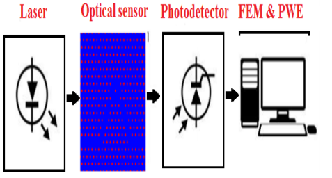
Fig 2 represents the schematic diagram of Phc based sensor. The input signal (Port 1) propagates into the photonic crystal sensor. The light is well handled by this sensor with respect to the refractive index variation of the pressure. After that, this light takes the path to the photodetector which is used as a converter from the optical signal into an electrical signal and the signal processing unit presents the detection quantity in readable form. The basic configuration of the structure is made of a linear waveguide by creating point defect and a hexagonal ring at the center acts a resonator, then the resonant wavelength is dropped from Port 1 to Port 2 (the output port).
Figure 2. Schematic diagram of PhC based sensor
Three parameters are important in sensing such as , refractive index of material (n), lattice constant (a) and ratio of radius to lattice constant (r/a) if any change in geometry by the application of external pressure, the photonic band gap will affected by some changes which will shifts the resonance wavelength of sensor[52].
In order to determine the refractive index 'n' of the constrained design, we used the optical tensor coefficients for silicon (Si) which are characterized by the stress-optical tensor equation [58]:
$\left[\begin{array}{l}n_{x x} \\ n_{y y} \\ n_{z z} \\ n_{y z} \\ n_{x z} \\ n_{x y}\end{array}\right]=\left[\begin{array}{l}n_0 \\ n_0 \\ n_0 \\ 0 \\ 0 \\ 0\end{array}\right]-\left[\begin{array}{llllll}C_1 & C_2 & C_2 & 0 & 0 & 0 \\ C_2 & C_1 & C_2 & 0 & 0 & 0 \\ C_2& C_2 & C_1 & 0 & 0 & 0 \\ 0 & 0 & 0 & 0 & 0 & 0 \\ 0 & 0 & 0 & 0 & 0 & 0 \\ 0 & 0 & 0 & 0 & 0 & 0\end{array}\right]\left[\begin{array}{l}\sigma_{x x} \\ \sigma_{y y} \\ \sigma_{z z} \\ \sigma_{y z} \\ \sigma_{x z} \\ \sigma_{x y}\end{array}\right]$
Here, $n_{i j}$ denotes the refractive index along (ij) direction, $n_0$ represent the refractive index ' $\mathrm{n}$ ' in zero-pressure, also, $\sigma_{i j}$ is called the pressure along (ij) direction. We suppose that pressure ' $\mathrm{P}$ ' is applied in 1-direction, therefore:
$\sigma_{x y}=\sigma_{x z}=\sigma_{y z}=0$ (1)
$\sigma_{x x}=\sigma_{y y=} \sigma_{z z}=\sigma$ (2)
In this way the value of ‘n’ modified by pressure ‘P’ reduces to:
$n=n_0-\left(C_1+2 C_2\right) \sigma$ (3)
where $C_1$ is defined as:
$C_1=\frac{n_0^3\left(P_{11}-2 V P_{12}\right)}{2 E}$ (4)
And $C_2$ is defined as:
$C_1=\frac{n_0^3\left[\left(P_{12}-V\left(P_{11}+P_{12}\right)\right]\right.}{2 E}$ (5)
Knowing that E represents Young's modulus and V is called Poisson’s ratio. Also, $P_{i j}$ denotes strain-optic constant. And for silicon its value is 130GPa and V is 0.255. In Pressure sensor, the applying pressure has a linear relationship with the refractive index of the proposed structure. By applying 1GPa pressure, the refractive index of a sensor is increased by $\approx$ 0.04 [59].
In this procedure, the optical source reacts as a transducer that converts the electrical signal into an optical signal and will be emitted thereafter through the crystal photonic based sensor. This sensor is used to maneuver the light with respect to the refractive index variation of the pressure. In that case, the photodetector received the light, which is also reacting as an inverse transducer convert optical signal into electrical signal. The sensed quantity of light signal will be detected by signal processing units in the legible form.
The two-dimensional finite-element method (F.E.M) is applied to simulate propagation, the total energy density (TED), the power flow norm (PFN) at the resonance and transmission of electromagnetism wave in waveguide by using COMSOL MULTIPHYSICS software and the band gap calculation is done by plane wave expansion method by using MATLAB software.
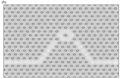
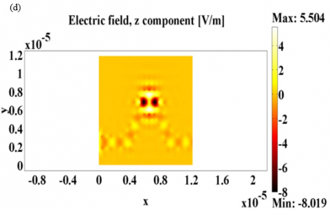
Fig.3 (a) and Fig.(b), show the distribution of refractive index and mesh along the structure (pressure sensor) based on photonic crystal. Thus, Fig.4 illustrates the result of the simulation of the distribution of the electric field in 2D and 3D through the pressure sensor at the resonance wavelength, λ_ resonance = 1.54 µm. The interaction between the wave propagated in the waveguide and the hexagonal ring resonator results in the change in the transmission spectrum.
Figure 3. (a), the distribution of the refractive index and (b), mesh of the proposed structure
Figure 4. (c), (d) and (e): the distribution of the electric field of the proposed sensor in 2D and 3D respectively at the resonance wavelength: λ_ resonance = 1.54 µm
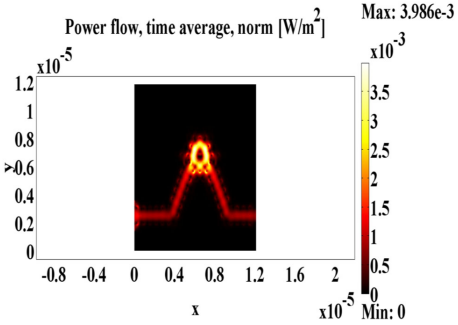
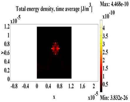
Also, Fig.5 and Fig.6 represent two important quantities which are the total energy density (TED) and the power flow norm (PFN) at resonance respectively.
Figure 5. The power flow norm at resonance
Figure 6. The total energy density at resonance
To analyze pressure effect on the structure, we perform comprehensive simulation study. The simulations have been performed in different pressures from 0 to 4GPa by $\approx$ 04 increments at each step, and corresponding resonant wavelengths obtained with different curves are depicted in Fig.7.
It has been observed that the resonant wavelength shifts to larger wavelength region when the refractive index is incremented. As example, from Table.1, 1GPa pressure, the refractive index of “Si” changes and pass from 3.46 at zero pressure to 3.50 at 1GPa, and therefore the resonant wavelength shifts from 1549nm to1553.6. In 2GPa pressure, the refractive index is calculated as 3.54.
Table 1. Resonance wavelengths and sensitivity at various pressures
|
Applied pressure (GPa) |
Refractive Index (n) |
Resonance Wavelength (nm) |
Sensitivity (nm/GPa) |
|
0 |
3.46 |
1549.0 |
-.- |
|
1 |
3.50 |
1553.6 |
4.6 |
|
2 |
3.54 |
1558.2 |
4.6 |
|
3 |
3.58 |
1562.8 |
4.6 |
|
4 |
3.62 |
1567.6 |
4.8 |
The functional schematic diagram presented in Fig.7 is indeed that of the pressure sensor based on photonic crystals (Phc) ring resonator. From Port1, the input signal (light wave (continuous Gaussian)) propagates through the sensor to port 2. This sensor as we explain before is manipulates the light following the variation of the refractive index of the pressure. Then through a photo-detector this light follows its path in order to be converted from an optical signal to an electrical signal and the signal processing unit presents the detection quantitative in a readable form. The initial configuration of this sensor is formed by linear waveguide by creating a point defect and a hexagonal ring in the center which acts as a resonator, then there λ_ (resonance) is removed from port 1 to port 2 which represents the port of exit.
Figure 7. Configuration diagram of a photonic crystal ring resonator (PCRR)-based sensor for pressure detection
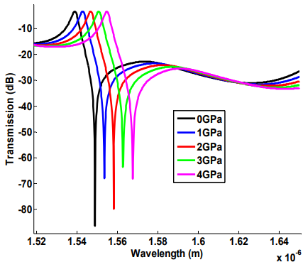
Then, Fig. 8 shows the transmission spectrum of the sensor in dB. When no pressure is applied to the sensor (0 GPa), the transmission is -86.49 dB, no stress is distributed over the surface of the pressure sensor; consequently the refractive index of the sensor remains the same where n = 3.46 (see Table.1) in this case the optical properties of the sensor do not change and the resonance wavelength of the sensor is 1.549µm. This Fig. 7 shows the transmission spectrum of the pressure sensor at different pressures such as 1, 2, 3 and 4 GPa and which displays the transmission values of -67.97 dB, 79.91dB, -63.53 dB and -68.19 dB respectively. In this condition, the variation in the applied pressure causes the resonant wavelength of the sensor to shift.
Figure 8. Transmission spectra for different pressures from 0 to 4GPa
From Fig.9, by analyzing the results, we observe that there is a linear relationship between the applied pressure as a function of the resonance wavelength and the refractive index. Then we can estimate the sensitivity of the sensor at 4.6nm /GPa.
Since the resonant peak has a very narrow linewidth, the resolution can be quite high. Fig.9 indicates an excellent linear relationship between pressure and resonant wavelength shift. This curve also indicates a wide dynamic range for this sensor from 0 to4 pressure.
Figure 9. Linear relationship between resonance wavelength, refractive index and pressure in the range 0 to 4GPa
In this paper, a novel 2D photonic crystal waveguide and hexagonal ring resonator sensor is designed, constructed and presented for pressure sensing. By changing optical properties of Si, the refractive index changes, and therefore, resonant wavelength shift. It is noticed that the resonant wavelength is shifted to the longer wavelength while increasing the pressure. In the absence of pressure the resonant wavelength is 1549nm and the sensitivity is 4.6nm/GPa. With emphasis on this point, the sensor can be calibrated to measure applied pressure. The designed sensor has a wide linearity range between 0 to 4GPa.The designed sensor has dielectric rods suspended in an air structure with dimensions of 11,837 × 11,837 $\mu \mathrm{m}^2$ . The photonic sensor is an intelligent and compact sensing device which can provide the possibility of using it in a magnetic field environment. Also, these types of refractive index sensors can be used in many detection applications such as humidity, stress sensors, etc.
The present work was supported by the Ministry of Higher Education and Scientific Research of Algeria.
[1] Baranwal, J., Barse, B., Gatto, G., Broncova, G, and Kumar, A. (2022). "Electrochemical Sensors and Their Applications: A Review" Chemosensors 10, no. 9: 363. https://doi.org/10.3390/chemosensors10090363
[2] Williams, D. E. (2020). Electrochemical sensors for environmental gas analysis. Current Opinion in Electrochemistry. https://doi.org/10.1016/j.coelec.2020.06.006
[3] Buryakov, I.A., Buryakov, T.I. & Matsayev, V.T. (2016) .Electrical, electrochemical, and thermometric sensors for the detection of explosives. J Anal Chem 71, 234–242. https://doi.org/10.1134/S1061934816030023
[4] Tounsi, A., Midhat, L., El Ghazali, A., Ouatiki, E., El Idrissi, M. (2022). Electrochemical Sensors for Food Quality and Safety. In: Chatoui, H., Merzouki, M., Moummou, H., Tilaoui, M., Saadaoui, N., Brhich, A. (eds) Nutrition and Human Health. Springer, Cham. https://doi.org/10.1007/978-3-030-93971-7_9
[5] Willett, M. (2014). Oxygen Sensing for Industrial Safety — Evolution and New Approaches. Sensors, 14, 6084- 6103. https://doi.org/10.3390/s140406084
[6] Kannan Pasupathikovil Ramaiyan and Rangachary Mukundan (Mukund) 2019 Electrochem. Soc. Interface 28. https://dx.doi.org/10.1149/2.F08193IF
[7] Ghoumazi, M., Bella, Mourad. Part.1: Influence of the Refractive Index on a Sensor Based On TwoDimensional Photonic Crystals.3rd International Conference on Applied Engineering and Natural Sciences (ICEANS’22) At: 20-23 July 2022, ISBN: 978-625-00-0830-0.At: Konya, Turkey.
[8] Parandin, F., Heidari, F., Aslinezhad, M. et al. (2022). Design of 2D photonic crystal biosensor to detect blood components. Opt Quant Electron 54, 618. https://doi.org/10.1007/s11082-022-03945-9
[9] Xia, J.; Qiao, Q.; Zhou, G.; Chau, F.S.; Zhou, G. (2020). Opto-Mechanical Photonic Crystal Cavities for Sensing Application. Appl. Sci., 10, 7080. https://doi.org/10.3390/app10207080
[10] Almawgani, A.H.M., Taya, S.A., Doghmosh, N. et al. (2023). A photonic crystal based on porous silicon as a chemical sensor for the detection of methanol compound. Indian J Phys. https://doi.org/10.1007/s12648-023- 02665-4
[11] Britto, E.C., Nizar, S.M. & Krishnan, P. (2022). A Highly Sensitive Photonic Crystal Fiber Gas Sensor for the Detection of Sulfur Dioxide. Silicon 14, 12665–12674. https://doi.org/10.1007/s12633-022-01982-3
[12] Fan J, Qiu L, Qiao Y, Xue M, Dong X, Meng Z. (2021). Recent Advances in Sensing Applications of Molecularly Imprinted Photonic Crystals. Front Chem. Jun 14; 9:665119. https://doi.org/10.3389/fchem.2021.665119
[13] P.R. Yashaswini, H.N. Gayathri, P.C. Srikanth. (2021). Performance analysis of photonic crystal based biosensor for the detection of bio-molecules in urine and blood, Materials Today: Proceedings, ISSN2214-7853. https://doi.org/10.1016/j.matpr.2021.06.192
[14] Ghoumazi, M., Bella, M., Hameurlain, M. (2022). Designing of a novel nanophotonic structure based on 2D photonic crystals for the detection of different materials. Mathematical Modelling of Engineering Problems, Vol. 9, No. 1, pp. 19-26. https://doi.org/10.18280/mmep.090103
[15] Sridarshini, T and Gandhi, S.I. (2020). Photonic band structure of 2D photonic crystals—a comparative study. Laser Phys. 30 026205. https://doi.org/10.1088/1555- 6611/ab5795.
[16] Arunkumar, R., Suaganya, T. & Robinson, S. (2019). Design and Analysis of 2D Photonic Crystal Based Biosensor to Detect Different Blood Components. Photonic Sens 9, 69–77. https://doi.org/10.1007/s13320- 018-0479-8.
[17] Ghoumazi, M., Abdesselam H., Hameurlain, M., Boudaa, M. (2018). Novel design of optical sensor based on two-dimensional photonic crystals for the detection of volatile organic compounds that can infect human health. Medical Technologies Journal, 2(4): 293-300. https://doi.org/10.26415/2572-004X-vol2iss4p293-300.
[18] Gamare, K and BalaJain, R. (2019). Performance analysis of 2D photonic crystal with line defect", AIP Conference Proceedings 2166, 02001. https://doi.org/10.1063/1.5131598.
[19] D H Ge et al (2017). Effect of Point and Linear Defects on Band-gap Properties in Triangular-Honeycomb Structure Photonic Crystals. IOP. Conf. Ser.: Mater. Sci.Eng. 170 012005. https://doi.org/10.1088/1757-899X/170/1/012005.
[20] Xavier, S.C, Carolin, B.E., Kabilan, A.P., Johnson, W. (2016). Compact photonic crystal integrated circuit for all-optical logic operation. Volume10, Issue 4.Pages: 142-147. https://doi.org/10.1049/iet-opt.2015.0072.
[21] Liu, Y., and Salemink, H. W. M. (2012). Photonic crystal-based all-optical on-chip sensor," Opt. Express Vol. 20, Issue 18, pp. 19912 - 19920. https://doi.org/10.1364/OE.20.019912.
[22] Ran, Z., He, X., Rao, Y. et al. (2021). Fiber-Optic Microstructure Sensors: A Review. Photonic Sens 11, 227–261. https://doi.org/10.1007/s13320-021- 0632-7
[23] Sánchez, A., Cortés, A., Porta, A.V. et al. (2023). Study on the Microstructure of a Photonic Crystal Fiber using the Elasto- Optical Effect. Silicon. https://doi.org/10.1007/s12633-023-02472-w
[24] Park S-W., Yeo, C.II., Kim, H. J., Kang, H. S., I. Seo, IJ., and Park, H.J. (2021), "Fiber optic sensor network for a monitoring and diagnosis system of the underground 22.9K XLPE cable," in Optical Fiber Communication Conference (OFC), P. Dong, J. Kani, C. Xie, R. Casellas, C. Cole, and M. Li, eds., OSA Technical Digest (Optica Publishing Group, 2021), paper Tu6C.4. https://doi.org/10.1364/OFC.2021.Tu6C.4.
[25] Portosi, V.; Laneve, D.; Falconi, M.C.; Prudenzano, F. (2019). Advances on Photonic Crystal Fiber Sensors and Applications. Sensors, 19, 1892. https://doi.org/10.3390/s19081892.
[26] Ghoumazi, M., Hameurlain, M. (2021). Study and simulation of a sensor based on 2D photonic crystals for the detection of aromatic compounds: C6H5I, C6H5F and C6H5Cl. In Annales de Chimie-Science des Matériaux, 45(4): 335-339. https://doi.org/10.18280/acsm.450409.
[27] Abadla, M.M., Elsayed, H.A. & Mehaney. (2021). A. Novel Design for the Temperature Sensing Using Annular Photonic Crystals. Silicon 13, 4737–4745. https://doi.org/10.1007/s12633-020-00788-5.
[28] Ghoumazi, M., Hocini, A. (2019). Design of bio-alcohol sensor based on two-dimensional photonic crystal in a nanophotonic structure. In 2019 International Conference on Advanced Electrical Engineering (ICAEE), 1-6. https://doi.org/10.1109/ICAEE47123.2019.9015129.
[29] Biswas, U., Bharti, G.K., Rakshit, J.K. (2020). Design of Photonic Crystal Based Optical Sensor for Analyzing Water Content in Milk. In: Dawn, S., Balas, V., Esposito, A., Gope, S. (eds) Intelligent Techniques and Applications in Science and Technology. ICIMSAT 2019. Learning and Analytics in Intelligent Systems, vol 12. Springer, Cham. https://doi.org/10.1007/978-3-030-42363-6_17.
[30] Li B., Hsiao F.-L., Lee C. (2011). Configuration analysis of sensing element for photonic crystal based NEMS cantilever using dual nano-ring resonator Li B., Sensors and Actuators, A: Physical, 169 (2) , pp. 352-361. https://doi.org/10.1016/j.sna.2011.03.020.
[31] Cheng, L.; Wang, R.; Hao, X.; Liu, G. (2021). Design of Flexible Pressure Sensor Based on Conical Microstructure PDMS –Bilayer Graphene. Sensors, 21, 289. https://doi.org/10.3390/s21010289
[32] R. Marma and M. A. Mollah. (2019).Gold Coated Microstructure Optical Fiber Based Plasmonic Bio - sensor," 2019 4th International Conference on Electrical Information and Communication Technology (EICT), 2, pp. 1-6. https://doi.org/10.1109/EICT48899.2019.9068778.
[33] Peng, J.; Jia, S.; Bian, J.; Zhang, S.; Liu, J.; Zhou, X.( 2019).Recent Progress on Electromagnetic Field Measurement Based on Optical Sensors. Sensors, 19, 2860. https://doi.org/10.3390/s19132860.
[34] Cai,Y & al (2020). Sensitivity enhancement of WS2- coated SPR-based optical fiber biosensor for detecting glucose concentration. Chinese Phys.B. Vol. 29(11): 110701. https://doi.org/10.1088/1674-1056/aba601.
[35] Sundhar, A., Valli, R., Robinson, S., Abinayaa, A and SivaBharathy, C. (2019).Two Dimensional Photonic Crystal Based Bio Sensor for Cancer Cell Detection," 2019 IEEE International Conference on System, Computation, Automation and Networking (ICSCAN), pp. 1-3. https://doi.org/10.1109/ICSCAN.2019.8878856
[36] Olyaee, S., Seifouri, M., Karami, R. et al.(2019).Designing a high sensitivity hexagonal nanocavity photonic crystal resonator for the purpose of seawater salinity sensing. Opt Quant Electron 51, 97. https://doi.org/10.1007/s11082-019-1778-z .
[37] Poonam, S., and Sharan P. (2015).Design of photonic crystal based ring resonator for detection of different blood constituents.” Optics Communications 348 19-23. https://doi.org/10.1016/j.optcom.2015.03.015.
[38] Y. Chen, W. S. Fegadolli, M. Jones, A. Scherer, and M. Li.(2014).Nanobeam photonic crystal cavity based multifunctional gas-phase chemical sensor," in CLEO: 2014, OSA Technical Digest (online) (Optica Publishing Group, 2014), paper SM3E.5. https://doi.org/10.1364/CLEO_SI.2014.SM3E.5.
[39] Olyaee, S., Najafgholinezhad, S. Alipour Banaei, H. (2013). Four-channel label-free photonic crystal biosensor using nanocavity resonators. Photonic Sens 3, 231–236. https://doi.org/10.1007/s13320-013-0110-y.
[40] Zhang, Y., Liu, P., Zhang S, Liu, W., Chen, J., and Shi, Y. (2016). High sensitivity temperature sensor based on cascaded silicon photonic crystal nanobeam cavities. Opt. Express 24, 23037 - 23043. https://doi.org/10.1364/OE.24.023037 .
[41] Shanthi K-V., Robinson, S. (2014). Two-dimensional photonic crystal based sensor for pressure sensing. Photonic Sens 4, 248 – 253. https://doi.org/10.1007/s13320-014-0198-8 .
[42] Wang, D., Tan, Qinggui., Li, Xiaojun., Ge, Jinman., Jiang, Wei., Liang, Dong and Cai, Haiwen. (2019). Analysis of mode characteristics of fiber Bragg gratings in large-mode-area double-clad fibers. J. Opt. Soc. Am. B 36, 768-774. https://doi.org/10.1364/JOSAB.36.000768
[43] Lin H., Xu, Y., Mumtaz , F., Dai, Y. and Zhou, A. (2019), Cascaded Fabry–Pérot Interferometers with Vernier Effect for Gas Pressure Measurement," 18th International Conference on Optical Communications and Networks (ICOCN), 2019, pp. 1-3. https://doi.org/10.1109/ICOCN.2019.8934785.
[44] Kim, H-T., Yu M. (2016).Cascaded ring resonator-based temperature sensor with simultaneously enhanced sensitivity and range. Opt. Express 24, 9501-9510. https://doi.org/10.1364/OE.24.009501
[45] Hillmer, H.; Woidt, C.; Kobylinskiy, A.; Kraus, M.; Istock, A.; Iskhandar, M.S.Q.; Brunner, R.; Kusserow, T.(2021).Miniaturized Interferometric Sensors with Spectral Tunability for Optical Fiber Technology—A Comparison of Size Requirements, Performance, and New Concepts. Photonics 2021, 8, 332. https://doi.org/10.3390/photonics8080332.
[46] Ghoumazi, M., Hocini, A. (2021). Photonic crystal based bio-sensor detection in nanophotonic structure using FEM method. International Journal of Sensors Wireless Communications and Control, 11(2): 216-224. https://doi.org/10.2174/2210327910666191218125109 .
[47] Ghoumazi, M., Hocini, A., Hameurlain, M. (2018). Study and simulation of the power flow distribution of an optical channel drop filter in structure based on photonic crystal ring resonator for different organic liquids. In International Conference in Artificial Intelligence in Renewable Energetic Systems, pp. 544- 551.https://link.springer.com/chapter/10.1007/978-3- 030-04789-4_58 .
[48] T-R Y., Kumar,R-R., T,S., Kandoth, A., John, K., Ramakrishnan, R-K., Das P-P., T,B., S, M., Hegde, G, S,T.(2017).Photonic crystal ring resonator: a promising device for a multitude of applications," Proc. SPIE 10108, Silicon Photonics XII, 101081J. https://doi.org/10.1117/12.2252702
[49] Wang, J et al. (2020). Novel fiber Mach-Zehnder interferometer based on three micro-silica spheres and photonic crystal fiber," 2020 Asia Communications and Photonics Conference (ACP) and International Conference on Information Photonics and Optical Communications (IPOC), pp. 1-3. https://doi.org/10.1364/ACPC.2020.M4A.62.
[50] Granpayeh, A., Habibi, H., Parvin, P. (2019). Photonic crystal directional coupler for all-optical switching, tunable multi/demultiplexing and beam splitting applications’. Journal of Modern Optics Volume 66, Issue 4; Pages 359 - 366. https://doi.org/10.1080/09500340.2018.1511859
[51] Mallika, C.S., Bahaddur, I., Srikanth, P.C., Sharan, P. (2015). Photonic crystal ring resonator structure for temperature measurement. Optik.Volume 126, Issue 20, October 2015, Pages 2252 - 2255. https://doi.org/10.1016/j.ijleo.2015.05.123
[52] S. Olyaee and A. A. Dehghani.(2012).Nano-pressure sensor using high quality photonic crystal cavity resonator," 2012 8th International Symposium on Communication Systems, Networks & Digital Signal Processing (CSNDSP), pp. 1-4.
[53] Xu, Z., Cao, L., Su, P., He, Q., Jin, G. and Gu, G. (2007). Micro - Displacement Sensor with Large Dynamic Range Based on Photonic Crystal Co-Directional Coupler," in IEEE Journal of Quantum Electronics, vol. 43, no. 2, pp. 182-187. https://doi.org/10.1109/JQE.2006.886449.
[54] Sun, Lixun., Zhang, Yuquan., Zhang, Chonglei., Dai, Yanmeng., Xin, Ziqiang., Zhu, Siwei., Yuan, Xiaocong., Min, Changjun., and Yang, Yong. (2019). Refractive index sensing and imaging based on polarizationsensitive graphene.Opt. Express 27, 29273-29286. https://doi.org/10.1364/OE.27.029273.
[55] Lee, C-W., Suh, J-M., Jang, H-W. (2019). Chemical Sensors Based on Two-Dimensional (2D) Materials for Selective Detection of Ions and Molecules in Liquid. Frontiers in Chemistry Vol. (7). ISSN=2296-2646. https://doi.org/10.3389/fchem.2019.00708.
[56] Stomeo, T et al, (2007).Fabrication of force sensors based on two-dimensional photonic crystal technology,” Microelectronic Engineering, vol. 84, no. 5–8, pp. 1450– 1453. https://doi.org/10.1016/j.mee.2007.01.227.
[57] Mai, T-T., Hsiao, F., Lee, C., Xiang, W., Chen, C., and Choi, W-K. (2011).Optimization and comparison of photonic crystal resonators for silicon microcantilever sensor,” Sensors and Actuators A, vol. 165, no. 1, pp.16– 25. https://doi.org/10.1016/j.sna.2010.01.006 .
[58] Olyaee, S., Dehghani, A.A. (2012). High resolution and wide dynamic range pressure sensor based on twodimensional photonic crystal. Photonic Sens 2, 92–96. https://doi.org/10.1007/s13320-011-0044-1.
[59] Upadhyay, S., Kalyani, V.L., Charan, C. (2015). Efficient designing and optimization of nano-cavity photonic crystal based pressure sensor. IJSRDInternational Journal for Scientific Research & Development| Vol. 3, Issue 06, 2015 | ISSN (online): 2321-0613.