Daosen Liu* | Shengsheng Wei | Dejun Wang
© 2022 IIETA. This article is published by IIETA and is licensed under the CC BY 4.0 license (http://creativecommons.org/licenses/by/4.0/).
OPEN ACCESS
Graphene is an excellent piezoresistive material. The gauge factor of graphene mirrors the sensitivity of electromechanical devices. This paper mainly studies the gauge factors of different layers of graphene under different deformation conditions. Specifically, a theoretical model was combined with linearized Boltzmann transport equation, and the density function theory (DFT) to explore how the layer number of graphene affects sensitivity. The results show that monolayer graphene is slightly more sensitive than two-layer graphene, and significantly more sensitive than three-layer graphene and four- layer graphene. In particular, monolayer graphene remains highly sensitive under large deformation conditions, which gives monolayer graphene a significant advantage over other layers of graphene. Furthermore, a microelectromechanical system (MEMS) pressure sensor was proposed with monolayer graphene, and compared with previous similar sensors with multilayer graphene in terms of sensitivity.
gauge factor, monolayer graphene, multilayer graphene, microelectromechanical system (MEMS), sensitivity
Graphene, which was experimentally discovered in 2004 [1, 2] is more robust and flexible than other materials. This novel material has attracted a lot of scientific interests [3-6] and becomes significant topics. A number of excellent properties have been found theoretically and experimentally [7-10], making graphene a very promising material in various fields. So far, a great amount of effort has been invested to apply graphene in electronic devices, such as flexible touch screens [11], high frequency transistors [12], and high sensitivity sensors [13-15]. The development of electronic devices is primarily motivated by the continuous improvement of performance. Therein, sensitivity is a key evaluator of the performance of electronic devices. The gauge factor mirrors the sensitivity of electronic devices, which are designed using the electromechanical properties of graphene. To make these devices more sensitive, many researchers have probed deep into the gauge factor of graphene.
Previous experiments on the gauge factor of graphene show that the factor is negatively correlated with the number of layers [16, 17]. Various ways have been adopted to modulate the gauge factor of graphene, such as modifying active molecules on the surface [18], changing the morphology or sensing mechanism [19], and doping graphene. Despite the extensive experimental works, the experimental data were obtained under specific experimental conditions, and are susceptible to environmental factors, which are difficult to eliminate. To make matters worse, graphene is extremely sensitive to environmental factors like temperature, humidity and gas adsorption. To capture the exact sensitivity of graphene, it is important to remove the influence of environmental factors. In particular, the effect of the layer number on the sensitivity of graphene must be studied theoretically, in order to guide the design of graphene-based electronic devices.
This paper presents a theoretical model using linearized Boltzmann transport equation. Drawing on the density function theory (DFT), the gauge factors of different layers of graphene were calculated under different deformation conditions, and used to evaluate the effect of the layer number on the sensitivity. On this basis, a microelectromechanical system (MEMS) pressure sensor was proposed with monolayer graphene, and compared with previous similar sensors with multilayer graphene in terms of sensitivity.
2.1 Theoretical analysis
The charge carrier density and mobility in strained graphene, and thus the gauge factor, can be described accurately by a theoretical model using linearized Boltzmann transport equation [20]. The charge carrier density in graphene is approximately proportional to the inverse of the squared Fermi velocity:
${{N}_{e}}(\varepsilon )\tilde{\ }1/{{v}_{F}}{{(\varepsilon )}^{2}}$ (1)
Considering the scattering mechanism of defects, the dependence of the mobility on the Fermi velocity can be given by:
${{\mu }_{e}}(\varepsilon )\tilde{\ }{{v}_{F}}{{(\varepsilon )}^{4}}$ (2)
Thus, the resistivity is approximately proportional to the inverse of the squared Fermi velocity [21]:
${{\rho }_{e}}(\varepsilon )\tilde{\ }1/{{v}_{F}}{{(\varepsilon )}^{2}}$ (3)
The resistance of a strained graphene can be defined by:
$R=\rho \frac{{{L}^{'}}}{{{W}^{'}}}=\frac{1}{2q{{N}_{e}}{{\mu }_{e}}}\frac{(1+{{\varepsilon }_{xx}})L}{(1+{{\varepsilon }_{yy}})W}$ (4)
where, $\varepsilon_{x x}$ and $\varepsilon_{y y}$ are strain components in the x and y directions of the graphene, respectively; q is the basic unit of charge; $L^{\prime}$ and $W^{\prime}$ are the length and width changes of the strained graphene, respectively.
In addition, the gauge factor, which reflects the sensitivity of the graphene material, can be determined by:
$G=\left| \frac{\Delta R}{{{R}_{0}}\varepsilon } \right|$ (5)
2.2 DFT calculation
To illustrate the sensitivity of graphene with different layers, a DFT method was employed to calculate the Fermi velocity of strained graphene. The primitive cell of each graphene system was constructed using two carbon atoms. Approximately 30 Å of vacuum was added onto the graphene to separate repeated cells along the c axis. To simply calculation, the graphene surface was meshed into k 10×10 grids using one mesh point along the c direction.
2.3 Device fabrication
The research team purchased a 0.5 mm-thick commercial single-crystal silicon wafer, which was grown in the [110], and obtained a Trivial Transfer Graphene from ACS Material, Nanjing XFNANO Materials Tech Co., Ltd. (XFNANO), which is a monolayer graphene coated by poly methyl methacrylate (PMMA).
The experimental devices were fabricated by the standard techniques. Firstly, the silicon nitride membrane was deposited to the thermally oxidized silicon wafer, forming a 200 nm-thick electrical isolation layer. Next, 50 nm of Cr and 250 nm of Au were evaporated to the silicon nitride layer for the contact. After that, the electrode patterning was acquired by photolithography and chemical etching. Again, it is pivotal to ensure that devices have the ability of electromechanical sensing. To this end, 1,400 μm-wide square cavities defined with photoresist were etched 450.3 μm deep into the silicon layer at the backside of the wafer. Then, a piece of glass was bonded with the wafer backside for sealing gas in the cavities, creating a pressure difference between the inside and outside of the cavities. In the end, the monolayer graphene was transferred onto the above-mentioned substrate. The graphene with PMMA was rinsed in de-ionized water and picked up with the chip. The chip was baked for 20 min at 100 ℃ such that the graphene adheres to the silicon nitride layer and the gold electrodes. Moreover, the PMMA was dissolved by acetone, followed by ethyl alcohol and de-ionized water rinsing. The chip was again baked for 10 min at 50 ℃ to dry the graphene. For imaging the graphene, its patterning was defined by photolithography and etched through an O2 plasma process.
2.4 Material characterization
In recent years, atomic force microscope and Raman spectrometer become powerful tools for characterizing and metering solid materials at the nanoscale. To verify the quality of graphene on the chip surface, these tools were employed to detect the roughness and layer number of graphene.
2.5 Measurement
The gas pressure was captured by referring to the readings on a Mensor pressure controller. In the Argon atmosphere, the positive gas pressure was loaded on an operating device, resulting in a pressure difference between the outside and inside of its cavity. The pressed cavity membrane then bent, causing the graphene to deform. In this way, the device sensing function is achieved. In addition, the electromechanical measurements were obtained by a multimeter, combined with the pressure controller.
According to Boltzmann's theory, the sensitivity of graphene can be explained by the relative change of Fermi velocities of the same material under different deformation conditions. The initial Fermi velocity varies with the layer number of graphene. In general, the monolayer graphene has a higher initial Fermi velocity than the other graphene systems. It is the difference between the initial Fermi velocities that results in the sensitivity difference between graphene systems.
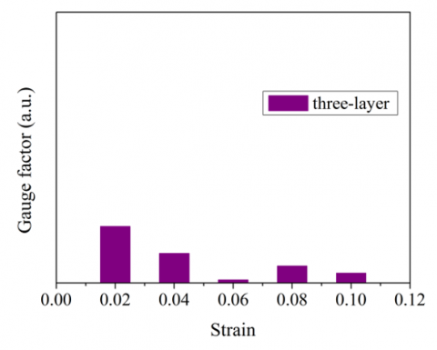
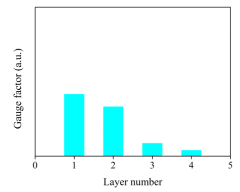
The gauge factors, an indicator of device sensitivity, for different layers of graphene were calculated by the theoretical model in Section 2.1 and compared in Figure 1. Figure 1(a) shows that the monolayer graphene was highly sensitive under all strain conditions. In particular, its sensitivity remained high despite serious deformations, giving monolayer graphene a significant advantage over other layers of graphene. Figure 1(b) shows that the two-layer graphene was not as sensitive as monolayer graphene across the range of strains. The sensitivity of the two-layer graphene was low under partial strain conditions. Figure 1(c) shows that the three-layer graphene had a low sensitivity across the entire strain range. The sensitivity was particularly low in the presence of large deformation. Figure 1(d) shows that the four-layer graphene bore the same features as the three-layer graphene. Figure 2 summarizes the mean gauge factors in the strain range shown in Figure 1 to broadly compare the sensitivities of different layers of graphene. It can be seen that the monolayer graphene was slightly more sensitive than the two-layer graphene, and significantly more sensitive than the three-layer and four-layer graphene. These results provide a theoretical basis for improving the sensitivities of graphene electromechanical devices.
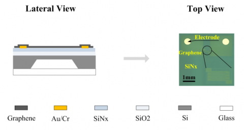
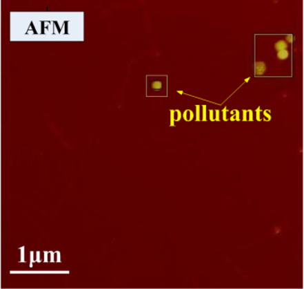
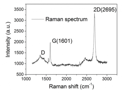
To test the sensitivity of the monolayer graphene, a sensitive element of graphene MEMS pressure sensor was fabricated by the standard techniques described in Section 2.3. The schematic of the device is shown in Figure 3. The lateral view provides the basic structure of the device. It can be seen that a multilayer component membrane, consisting of silicon and silicon dioxide and silicon nitride (SiNx), serves as the structural element in this pressure sensor. The suspended membrane was poised because the sealed cavity has the same pressure inside and outside, in the absence of external factors. When a differential pressure is applied, the membrane deflects and deforms into a concave shape. The top view in Figure 3 presents the pattern of the graphene on the SiNx membrane after being etched by O2 plasma. From the top view, it can be seen that the only resistance of the monolayer graphene exhibited a meander pattern. The graphene resistance was above the cavity, acting as sensitive element. The pressure was sensed when the only graphene resistance is strained, because the suspended membrane deforms due to the pressing device. The atomic force micrograph and the Raman spectrum of the graphene are shown in Figure 4. Although the micrograph indicates that the graphene is smooth, there were a few pollutants on the graphene surface. The Raman spectrum suggests that the monolayer graphene had few defects.
(a) Monolayer
(b) Two layers
(c) Three layers
(d) Four layers
Figure 1. Gauge factors of graphene
Figure 2. Mean gauge factor of graphene with different layers
Figure 3. Schematic of the basic device structure
(a) Atomic force micrograph of graphene
(b) Raman spectrum of graphene
Figure 4. Characterization of device
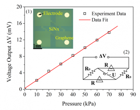
To evaluate the sensing performance of the device based on the only monolayer graphene resistance, a new pressure sensor was developed based on above sensitive element (Figure 5 (1)). It can be learned that the sensor consists of four monolayer graphene resistances with the meander patterns. These resistances are symmetric to the sensor center. The original values of these resistances are equal, for every meander pattern is as same as the one of only monolayer graphene resistance in Figure 3. Therein, a pair of graphene resistances above the cavity act as sensitive elements, but the rest are not above the cavity and remain constant. A direct current (DC) source and a multimeter were connected to the above circuit (Figure 5(2)), forming a Wheatstone bridge based on the monolayer graphene with meander patterns. The R in Figure 5(2) represents single graphene resistance as sensitive element, and the R0 represents constant graphene resistance. The voltage output ΔV of the Wheatstone bridge can be expressed as:
$\Delta V=2 U R_0 /\left(R_0+R\right)-U$ (6)
where, U is the voltage of the DC source. The electromechanical performance of the proposed sensor was measured by combining the electromechanical measurements for the only monolayer graphene resistance as sensitive element in Figure 3 and theoretical analysis by the equation (6) for this sensor [22]. As shown in Figure 5, the test data at 5 V demonstrate that the voltage output increased linearly as the differential pressure rose from 0 to 70 kPa. From Figure 5, it can be seen that the voltage output of the sensor could reach up to 14.1 mV when the pressure rose to 70 kPa. Its sensitivity was about 4.03×10⁻⁵/kPa. Figure 5 also provides the excellent fitting for the group data.
Figure 5. Voltage output as function of the differential pressure for the proposed sensor
In practice, graphene as a sensitive element shows different sensitivities, depending on the layer number. In this paper, monolayer graphene is taken to prepare the graphene MEMS pressure sensor, and the sensitivity of monolayer graphene is realized at about 4.03×10⁻⁵/kPa in device applications. Recently, few-layer graphene was used to prepare similar sensors, and its sensitivity was measured at 1.94×10⁻⁵/kPa in device applications [23]. Multilayer graphene was also adopted to prepare the similar sensors, and its sensitivity was around 3.33×10⁻⁵/kPa in device applications [24]. Thus, the device fabricated using monolayer graphene is more sensitive than the devices fabricated with few or multiple layers of graphene. This coincides with the above theoretical analysis that monolayer graphene is more sensitive than multilayer graphene.
In summary, this paper puts forward a theoretical model using linearized Boltzmann transport equation. To disclose the effect of the layer number on the sensitivity of graphene, we theoretically studied the gauge factors of different layers of graphene under different deformation conditions, by combining the model with the DFT. The results show that the monolayer graphene is highly sensitive under all strain conditions. By comparison, the monolayer graphene is slightly more sensitive than the two-layer graphene, and significantly more sensitive than the three-layer and four-layer graphene. In particular, the sensitivity of monolayer graphene remains high under large deformations, giving it a significant advantage over other layers of graphene. In addition, the superiority of monolayer graphene was verified by contrasting the proposed MEMS pressure sensor with previous similar sensors with multilayer graphene. The research results can guide the design of graphene electronic devices, and eliminate the blindness of experimental studies on device applications.
This work is supported by the Basic Research Business Expenditure for Undergraduate Institutions in Heilongjiang Province (Grant No.: 135409327) and Fundamental Research Funds of Heilongjiang Provincial Department of Education (Grant No.: 145109216).
[1] Novoselov, K.S., Geim, A.K., Morozov, S.V., Jiang,D., Zhang, Y., Dubonos, S.V., Grigorieva, I.V., Firsov, A.A. (2004). Electric field effect in atomically thin carbon films. Science, 306(5696): 666-669. http://dx.doi.org/10.1126/science.1102896
[2] Berger, C., Song, Z., Li, T., et al. (2004). Ultrathin epitaxial graphite: 2D electron gas properties and a route toward graphene-based nanoelectronics. The Journal of Physical Chemistry B, 108(52): 19912-19916. http://dx.doi.org/10.1021/jp040650f
[3] Tao, L. Q., Zhang, K. N., Tian, H., et al. (2017). Graphene-paper pressure sensor for detecting human motions. ACS nano, 11(9): 8790-8795. http://dx.doi.org/10.1021/acsnano.7b02826
[4] Wang, X., Wei, G.D. (2020). Quantum Scars in Microwave Dielectric Photonic Graphene Billiards. Chinese Physics Letters, 37(1): 014201. http://dx.doi.org/10.1088/0256-307X/37/1/014201
[5] Gu, Q., Xing, D., Sun, J. (2019). Superconducting single-layer T-graphene and novel synthesis routes. Chinese Physics Letters, 36(9): 097401. http://dx.doi.org/10.1088/0256-307X/36/9/097401
[6] Tamburrano, A., Sarasini, F., De Bellis, G., D’Aloia, A. G., Sarto, M.S. (2013). The piezoresistive effect in graphene-based polymeric composites. Nanotechnology, 24(46): 465702. http://dx.doi.org/10.1088/0957-4484/24/46/465702
[7] Bolotin, K.I., Sikes, K. J., et al. (2008). Ultrahigh electron mobility in suspended graphene. Solid state communications, 146(9-10): 351-355. http://dx.doi.org/10.1016/j.ssc.2008.02.024
[8] Morozov, S.V., Novoselov, K.S., Katsnelson, M.I., Schedin, F., Elias, D.C., Jaszczak, J.A., Geim, A.K. (2008). Giant intrinsic carrier mobilities in graphene and its bilayer. Physical review letters, 100(1): 016602. http://dx.doi.org/10.1103/PhysRevLett.100.016602
[9] Dorgan, V.E., Bae, M.H., Pop, E. (2010). Mobility and saturation velocity in graphene on SiO2. Applied Physics Letters, 97(8): 082112. http://dx.doi.org/10.1063/1.3483130
[10] Lee, C., Wei, X., Kysar, J. W., Hone, J. (2008). Measurement of the elastic properties and intrinsic strength of monolayer graphene. science, 321(5887): 385-388. http://dx.doi.org/10.1126/science.1157996
[11] Bae, S., Kim, H., Lee, Y., et al. (2010). Roll-to-roll production of 30-inch graphene films for transparent electrodes. Nature nanotechnology, 5(8): 574-578. http://dx.doi.org/10.1038/nnano.2010.132
[12] Lin, Y.M., Dimitrakopoulos, C., Jenkins, K.A., Farmer, D.B., Chiu, H.Y., Grill, A., Avouris, P. (2010). 100-GHz transistors from wafer-scale epitaxial graphene. Science, 327(5966): 662-662. http://dx.doi.org/10.1126/science.1184289
[13] Tian, H., Shu, Y., Wang, X.F., et al. (2015). A graphene-based resistive pressure sensor with record-high sensitivity in a wide pressure range. Scientific reports, 5(1): 1-6. http://dx.doi.org/10.1038/srep08603
[14] Fortunato, M., Bellagamba, I., Tamburrano, A., Sarto, M.S. (2020). Flexible Ecoflex®/graphene nanoplatelet foams for highly sensitive low-pressure sensors. Sensors, 20(16): 4406. http://dx.doi.org/10.3390/s20164406
[15] Cheraghi Bidsorkhi, H., D’Aloia, A.G., Tamburrano, A., De Bellis, G., Sarto, M.S. (2021). Waterproof Graphene-PVDF Wearable Strain Sensors for Movement Detection in Smart Gloves. Sensors, 21(16): 5277. http://dx.doi.org/10.3390/s21165277
[16] Chen, X., Zheng, X., Kim, J.K., Li, X., Lee, D.W. (2011). Investigation of graphene piezoresistors for use as strain gauge sensors. Journal of Vacuum Science & Technology B, Nanotechnology and Microelectronics: Materials, Processing, Measurement, and Phenomena, 29(6): 06FE01. http://dx.doi.org/10.1116/1.3660784
[17] Zheng, X., Chen, X., Kim, J.K., Lee, D. W., Li, X. (2013). Measurement of the gauge factor of few-layer graphene. Journal of Micro/Nanolithography, MEMS, and MOEMS, 12(1): 013009. http://dx.doi.org/10.1117/1.JMM.12.1.013009
[18] Chen, Z., Ming, T., Goulamaly, M. M., et al. (2016). Enhancing the sensitivity of percolative graphene films for flexible and transparent pressure sensor arrays. Advanced Functional Materials, 26(28): 5061-5067. http://dx.doi.org/10.1002/adfm.201503674
[19] Zhao, J., Zhang, G. Y., Shi, D.X. (2013). Review of graphene-based strain sensors. Chinese Physics B, 22(5): 057701. http://dx.doi.org/10.1088/1674-1056/22/5/057701
[20] Smith, A.D., Niklaus, F., Paussa, A., et al. (2016). Piezoresistive properties of suspended graphene membranes under uniaxial and biaxial strain in nanoelectromechanical pressure sensors. ACS nano, 10(11): 9879-9886. http://dx.doi.org/10.1021/acsnano.6b02533
[21] Wang, V., Xu, N., Liu, J.C., Tang, G., Geng, W.T. (2021). VASPKIT: A user-friendly interface facilitating high-throughput computing and analysis using VASP code. Computer Physics Communications, 267: 108033. http://dx.doi.org/10.1016/j.cpc.2021.108033
[22] Nakagawa, R., Wang, Z., Suzuki, K. (2018). Area-arrayed graphene nano-ribbon-base strain sensor. In ASME International Mechanical Engineering Congress and Exposition, 52156: V010T13A008. http://dx.doi.org/10.1115/IMECE2018-87277
[23] Wang, Q., Hong, W., Dong, L. (2016). Graphene “microdrums” on a freestanding perforated thin membrane for high sensitivity MEMS pressure sensors. Nanoscale, 8(14): 7663-7671. http://dx.doi.org/10.1039/C5NR09274D
[24] Zhu, S.E., Krishna Ghatkesar, M., Zhang, C., Janssen, G. C.A.M. (2013). Graphene based piezoresistive pressure sensor. Applied Physics Letters, 102(16): 161904. https://doi.org/10.1063/1.4802799