Laith M. Abduljabbar* | Mohammed H. Hwidi | Ahmed A. Alchalaby
© 2021 IIETA. This article is published by IIETA and is licensed under the CC BY 4.0 license (http://creativecommons.org/licenses/by/4.0/).
OPEN ACCESS
In this work, a pulsed laser deposition technique was used which is one of the modern methods of preparing thin films where zinc telluride was deposited on slices of glass using different Nd: YAG laser wavelengths (0.532 μm and 1.064 μm) .Two different laser energies (600 mJ and 900 mJ) were used to study its effects on the properties of Zinc Telluride films at room temperature. Measurement of X-Ray Diffraction (XRD) and Atomic Force Microscope (AFM) was used to demonstrate the structural and morphological properties of the prepared Zinc Telluride thin films which shows that the films consists of multiple crystals and its structural design is a cubic with a small crystallites size and dissimilar shapes . The optical properties in the range of (400-1000) nm using UV-VIS spectrophotometer were studied by transmission and reflection spectra where found that for Zinc Telluride films have more transmission in the range of visible spectrum which can be reach to greater than 90 % with wide band gap of 2.2 eV is a promising material to be used in photovoltaic devices as solar cells and detectors.
Zinc Telluride, Thin films, Nd: YAG laser, pulsed laser
Zinc telluride (ZnTe) compound usually has a cubic crystalstructure and has a direct energy gap semiconductor material with value of 2.27 eV at 300K; it is a very important semiconductor component in the II-VI family because it has a high absorption coefficient and low cost [1]. ZnTe is an important material for different optoelectronics device, such as colorful light emitting diodes and photovoltaic devices [2, 3]. Recently, increased the focusing in the study of Zinc telluride films and its components because of its many properties and features that can be exploited in several applications that can be used for solar cells and electronic semiconductor devices [4].
Different technical can be used for fabrication of ZnTe alloys such as electrical depositions [5], thermal deposition [6], thermal beam epitaxial [7], radiofrequency sputtering [8] ,and deposition using pulsed laser[9]. Pulsed Laser Deposition (PLD) technique used in the process of fabrication of the thin films become one of the very important techniques nowadays due to its simplify, versatility, inexpensive, very flexible and uses in the fabrication of thin films with high efficiency [10-13].
One of the main advantages of pulsed laser deposition is a congruent material transfer, which allows the deposition of complex structures, preserving the stoichiometry of the target material. Another advantage of the highly directed ablation flux is the efficiency of handling costly or toxic materials [14].
The zinc telluride (ZnTe) films will be deposited on a glassslides using pulsed laser deposition technique with different laser energies and wavelengths. Before the operation of deposited the target material, thin flat pieces of glass, typically 75 by 26 mm were used as substrates material were cleaned with acetone and distilled water then dried with an air gun.
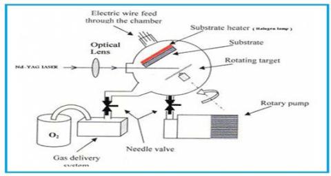
Pulsed laser deposition system as shown in (Figure 1) which consisted of a chamber which evacuated with a pressure of (0.001 mbar) and a constant substrate temperature 100 C0. Nd:YAG laser with wavelengths (0.532 μm , 1.064 μm) and laser energies (600 mJ , 900 mJ) and repetition rate (1 Hz) was used to deposited the ZnTe thin film on a glass substrate with constant pulses (30 pulse).
Figure 1. Schematic diagram of pulsed laser deposition system
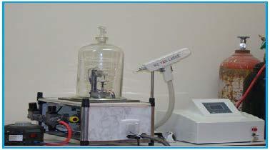
The measured distance between the centre of a lens and its focus was about (10 cm) and the distance between the material target which rotate at regular speed and the substrate material which connected with heater was about of (3 cm). The system setup of the PLD it was implemented in the laboratory can be shown in (Figure 2).
Figure 2. Experimental setup of PLD
After deposition process the diffractometer system (shimadzu - XRD 6000- Japan) with wavelength 15418Å and CuKα radiation using to identify the structural characterizations of the fabricated films. Morphological characterization of the ZnTe films was studied by using an Atomic Forces Microscopy technique (AFM). The optical properties such as transmission, reflection and energy band gap were measured using (UV-Visible 1800) spectrometer in the range (400-1000) nm.
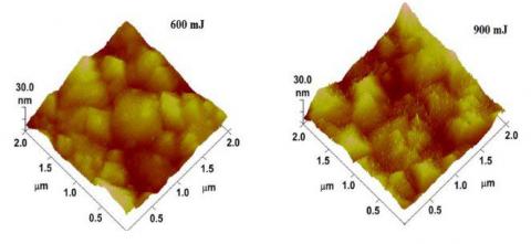
The AFM images of the fabricated films at wavelength0.532 μm for laser energies 600 mJ and 900 mJ can be shown in (Figure3 ) .From this figure, the films consists of a small crystallites with irregular shapes but the cumulation of the many crystal groups can be noticed that there is insufficient propgation of the crystal size of the atoms.
Figure 3. AFM pattern of the films at wavelength 0.532 μm using multi-laser energies
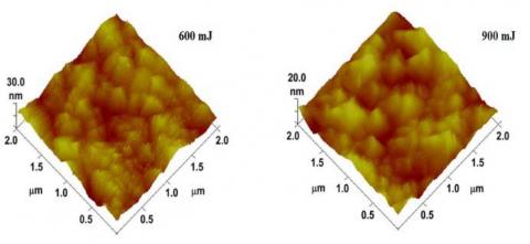
Figure 4 shows the AFM images of ZnTe thin films at wavelength 1.064 μm for energies 600 mJ and 900 mJ . From this figure the fabricated films has a grain size will be enlarges greatly with an increasing the amount of the laser energies from 600 mJ to 900 mJ and the grain shape becomes hazy due to the fast decomposition of the films on the substrates materials. The AFM characterization is in good agreement with [1] and [2] results.
Figure 4. AFM pattern of the films at wavelength 1.064 μm using multi-laser energies
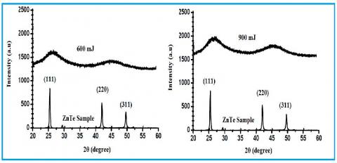
Figure 5 describe the X-Ray Diffraction (XRD) pattern of multi laser energies (600 mJ and 900 mJ) of ZnTe thin films at constant laser wavelength 0.532 μm. It can be seen that from XRD pattern of the thin films that it have a polycrystalline and cubic shapes and there are a three remarkable peaks (111) (220) and (311) and the distinguished peak was (111) this results was agree with studies [2],[3] and [9]. The Full Width at Half Maximum (FWHM) and the crystal size of the distinguished peak decreasing with increases of the laser energies because of the dropped of the defect which resulting of the shrink of the grain boundary of the crystal.
Figure 5. The X-ray diffraction patterns of ZnTe thin films at wavelength 0.532 μm.
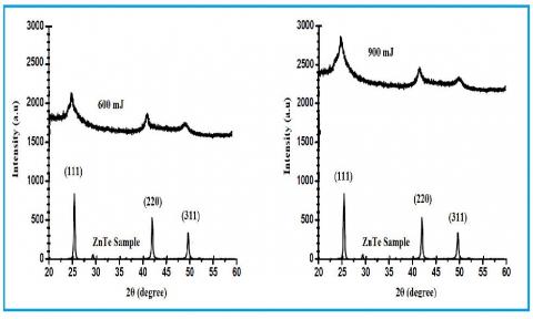
Figure 6 shows the XRD pattern of different laser energies (600 mJ and 900 mJ) of ZnTe thin films at constant laser wavelength 1.064 μm. It is observed that when the laser energy increased the large crystallite size has been decreased due to the fast growths of the crystal and by the reasons of the decreasing in grains boundary of it.
Figure 6. The X-ray diffraction patterns of ZnTe thin films at wavelength 1.064 μm
Scherer's equation can be utilize to compute the crystalline size (CS) of ZnTe fabricated films:
$\mathrm{CS}=\frac{0.94 \lambda}{\beta \cos \theta}$
Where λ is wavelength of the radiation beam, β is Full width at half maximum (FWHM) of the main peaks and θ is the angle of diffraction. Tables-1 and 2 shows the XRD parameters for ZnTe films at laser wavelength 0.532 μm and 1.064 μm with laser energies 600 mJ and 900 mJ.
Table 1. XRD parameters for ZnTe films at laser wavelength 0.532 μm
|
Laser Energy (m J) |
2θ(deg) |
dhkl(Å) |
β(deg) |
CS (nm) |
|
600 |
25.283 |
35.169 |
0.412 |
20.66 |
|
900 |
25.242 |
35.237 |
0.435 |
19.56 |
Table 2. XRD parameters for ZnTe films at laser wavelength 1.064 μm
|
Laser Energy (m J) |
2θ(deg) |
dhkl(Å) |
β(deg) |
CS (nm) |
|
600 |
25.294 |
35.198 |
0.422 |
20.17 |
|
900 |
25.261 |
35.341 |
0.447 |
19.04 |
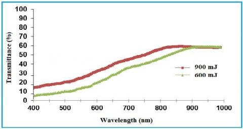
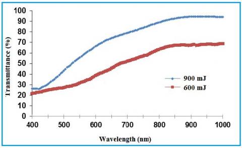
Figures 7 and 8 show the transmission spectrum of ZnTe thin films on glass slides which be fabricated by PLD at wavelength 0.532 μm and 1064nm respectively for multi laser energies. It is shown that the maximum value of the transmission is 60% for Zinc telluride thin films in the wavelength 0.532 μm while the value can reach to 90 % for Zinc telluride thin films in the wavelength 1.064 μm because of increasing in the densities of the films and due to high transparent which agree with the other studies [9].
Figure 7. Transmission of ZnTe films at wavelength 0.532 μm for multi laser energies
Figure 8. Transmission of ZnTe films at wavelength 1.064 μm for multi laser energies
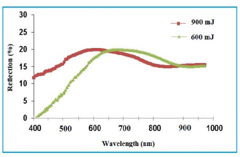
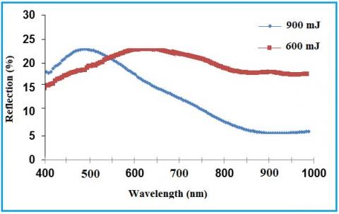
Figures 9 and 10 show the reflection spectrum of ZnTe thin films at wavelengths 0.532 μm and 1064nm respectively for the two laser energies (600 and 900) mJ . It can be observed that the reflection spectrum of all fabricated films were increasing quickly in the visible region and then decreased with the increasing of wavelength from (800 to 1000) nm with the increasing in laser energies.
Figure 9. Reflection versus wavelength of ZnTe films at wavelength 0.532 μm for various laser energies
Figure 10. Reflection versus wavelength of ZnTe films at wavelength 1.064 μm for various laser energies
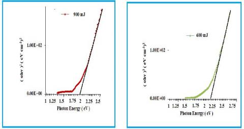
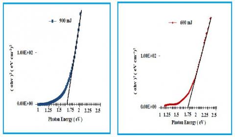
The amount of the optical energy of the prepared films was computed using the relation [7]:
$\alpha h v=\beta\left(h v-E_{g}\right)^{x}$
Where β is a Tauc constant, α is the coefficient of absorption, hv denote the incident light frequency, Eg is the direct band gap and x =1/2 yields linear dependence, which describe the linear transition depended on the nature of the material and the kinds of the transition. The energy band gap Eg can be obtaining from the interception of the axis of photon energy after extrapolated of the straight line of the curve of (αhν)2 versus (hv) plotting.
Figure 11 and Figure12 shows the amount of energy gap of ZnTe films at wavelengths 0.532 μm and 1.064 μm respectively for various laser energies.It can be observed that the energy gap of the films in the case of 0.532 μm laser wavelength reduced from [2.2 eV to 1.88eV] when the laser energy growth from 600 mJ to 900 mJ , while it is reduced from [1.75 eV to 1.62 eV] for the case of 1.064 μm laser wavelength when the laser energy growth from 600 mJ to 900 mJ this is because many levels of energies resulted in many imbrication in the energy of valence band and conduction band in the energy band gap of the prepared films. This imbrication in the bands due to the reduction of the energies of the several band gaps which can be observed in the lower band gap for increased laser energy is growth [10].
In addition to the above mentioned there are two reasons for the decrease in the energy band gap when the laser energy increases firstly; the increasing of laser-induced defects, which consequently narrows the energy band gap of the fabricated thin films. Secondly ; increase in the grain size of the films and this increase causes a decrease in the energy band gap.
Figure 11. Band gap energy value of ZnTe films at wavelength 0.532 μm for various laser energies
Figure 12. Band gap energy value of ZnTe films at wavelength 1.064 μm for various laser energies
Polycrystalline and cubic structure ZnTe thin films werefabricated using pulsed laser deposition technique with different laser energies and wavelengths. The grain size of the fabricated Zinc telluride thin films enlarges greatly with an increases of the laser energies from 600 mJ to 900 mJ with 0.532 μm laser wavelength while becomes hazy with 1.064 μm laser wavelength due to the fast decomposition of the films on the substrates materials. The maximum value of the transmission is 60% for Zinc telluride thin films in the wavelength 0.532 μm while the value is greater than 90 % for Zinc telluride thin films in the wavelength 1.064 μm due to increasing in the densities of the films and because of the high transparent which making this material to be used in photovoltaic devices as solar cells and detectors. The energy band gaps of the films were decreased when laser energy increased from 600 mJ to 900 mJ for both laser wavelengths 532nm and 1.064 μm.
[1] Hossain, M.S.; Islam, R. (2010). Structural, elementalcompositions and optical properties of ZnTe:V thinfilms. Chalcogenide Letters Vol. 7.
[2] Tanaka, T.; Matsuno, Y.J.; Kume, Y.; Nishio, M.;Guo, Q.X.; and Ogawa, H.(2004). Characterization ofAl doped ZnTe Layer Fabricated by Al ThermalDiffusion. Phys. Status Solidi B, 1, 1026.
[3] Bozzini, B.; Baker, M.A.; Cavallotti, P.L.; Cerri, E.;and Lenardi, C. (2000). Electro deposition of ZnTe forphotovoltaic cells. Thin Solid Films, 388, 361,2.
[4] Kazmerski, L.L. (1980). Polycrystalline andAmorphous Thin Films and Devices. Academic Press,New York.
[5] Ishizaki, T.; Ohtomo, T.; and Fuwa, A. (2004) Journalof Physics D: Applied Physics, 37, p. 255, 5.
[6] Aqili, A.K.S.; Ali, Z.; and Maqsood, A. (2000).Optical and structural properties of two-sourcedevaporated ZnTe thin films. Applied Surface Science,167, 1.
[7] Gunshor, R.L.; Koladziejski, L.A.; Otsuka, N.; andDutta, S. (1986). Surface Science. 174, 522.
[8] Bellakhder, H.; Outzourhit, A.; and Ameziane, E.L.(2001). Study of ZnTe thin films deposited by r.f.sputtering. Thin Solid Films, 382, 30.
[9] Ochoa-Estrella, F. J.; Vera-Marquina, A.; Mejia, I.;Leal-Cruz, A.L.; Pintor-Monroy, M.I.; and Quevedo-López, M. (2018). Structural, optical, and electricalproperties of ZnTe:Cu thin films by PLD. Journal ofMaterials Science: Materials in Electronics.
[10] Tawari, P.; Wu, X.; Foltyn, S.; Lee, M.L; andCampbell, J. (1994). Applied Physics Letters, 64 .
[11] Narayan, J.; Biunno, N.; Singh, R.; Holland, O.; andAuchiello, O. (1987). Applied Physics Letters, 51 -1845.
[12] Saenger, K. (1993) Proc. Adv. Mater. 2
[13] Graham K.H,. (1994). Pulsed laser deposition. MRSBulletin No. 2, Vol. XVII.
[14] Aydinli, A.; Compaann, A. (1993). AdvancedMaterials for Optics and Optoelectronics 2, 69-86.