Parimalasundar Ezhilvannan | Suresh Krishnan*
© 2020 IIETA. This article is published by IIETA and is licensed under the CC BY 4.0 license (http://creativecommons.org/licenses/by/4.0/).
OPEN ACCESS
This paper is dealing about Switched Capacitor Multi-Level Inverter (SCMLI) circuit which is controlled by triangular multicarrier Sinewave Pulse Width Modulation (SPWM) technique. The proposed SCMLI is powered from asymmetric DC source configuration to obtain multi-level output voltage by applying switching pulse to the main circuit from control circuit for switching operation. Fourteen switches and four capacitors are employing to do the proposed inversion operation in an effective way. Switching capacitors can perform boost operation to enhance voltage from the source level to the required level. Input DC from the asymmetric sources is converted to AC voltage for the application of consumers. This proposed conversion system is applicable for mainly in industrial and renewable energy-based energy conversion system because it can carry high output voltages. This proposed method gives about more efficiency. Also reduces switching losses in lower value, low conduction losses and capacitor ripple losses. The simulation model is analyzed in MATLAB/SIMULINK platform and the same validated in hardware results. The developed SCMLI structure is witness over other topologies for the power inversion process in the multi-level.
switched capacitor multi-level inverter, boost conversion, triangular multi-carrier sine wave pulse width modulation
At present, the inverters are playing a vital role in industrialized and in household applications [1]. Multilevel inverters are becoming workable DC-to-AC converting of power used for altered applications, like electrical drives, RECS applications, electric utilities, and filters [2]. For multiple application purposes a new SCMLI is developed [3]. For reliable working of inverters PWM techniques are preferable [4]. Another main drawback of conventional MLI is that they require extra supplementary circuit to maintain voltage as balanced at capacitors; this circuit amplifies its dimension, price and difficultness of converter [5]. Comparing with normal two-level inverters, the Multilevel Inverters shows many advantages, like producing synthesized output voltage, higher power production ability, low losses with high efficiency, less voltage strain across switching devices [6] those contains IGBTs, MOSFETs, power diodes, DC sources and capacitors [7]. In general, three usual Multi Level Inverter topologies are present, namely, Flying Capacitor (FC) Cascaded H-bridge (CHB) and diode clamped (DC) [8]. The latest Multi level inverter arrangement by way of more no. of steps linked by way of a small amount of power switching devices suggested [9]. The latest switched capacitor-diode structure is presented [10]. These sources can be the main for synthesized outputs [11]. It needs more capacitors in addition to as diodes on the way to generate heights levels of voltage at outputs [12]. On the way to defeat these problem supplementary circuits and composite controlling strategy has presented. The resonant switched capacitor converter is developed in this paper [13], which minimizes the capacitor voltage unbalance issues, drawbacks in amplify system as bulky, pricey and difficulty lacking the remaining advantage of self-voltage boost ability.
On the way to attain self-voltage boost capacity and ease the unbalanced capacitor voltage issue exclusive of taking supplementary circuit, SCMLI is presented in this paper. Here, capacitors are used to be as alternative DC voltage sources. The SCMLI can produce multiple levels of voltage output with minimum number of power switches and sources. In count, SCMLI also enhance its source voltage up to required level of load voltage with alternating switching of those capacitors [14]. Another main benefit of SCMLI is obtaining of capacitor voltage balance with the help of switching sequence tactic. The remaining part of this paper is structured in the following pattern.
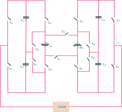
In this developed method, the capacitors of Ci1 with Ci1' can charge up to input voltage, while the capacitors of Ci2 & Ci2' can charge up to 4 times of input voltage with suitable triggering patterns. This indicates that the developed topology able to change the state of capacitors from charge and discharge simultaneously, that helpful to maintain voltage of capacitor at desired levels with lesser amount of voltage ripples. Figure 1 shows the developed SCMLI constructional details, which consists of 2 asymmetric DC voltage sources (Vi & 4Vi), 14 unidirectional switching devices either IGBTs or MOSFETs, and 4 Switching capacitor devices. The entire arrangement makes 21 stages of output voltage levels with the load terminals.
Figure 1. Developed SCMLI
2.1 Making a voltage level at zero
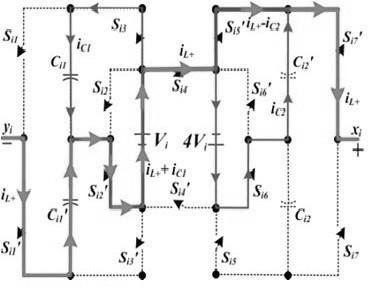
The output voltage at zero level was generated with turning ON the switches in the sequence of Si1', Si3', Si4', Si5, and Si7, the output voltage is appeared as zero in between load terminals. In this proposed topology, the capacitors Ci1' & Ci2 are arranged in charging condition by making a switch are turned ON in the pattern of Si2 and Si6' in that order but capacitors which is connected to the circuit Ci1& Ci2' are operated in the position of non-conduction mode, as shown in Figure 2.
Figure 2. Equivalent circuit of zero level voltage
2.2 Making a voltage level at ±2Vi
The switching sequences are operated in the pattern of switches Si1'to Si7' are switched ON, capacitor Ci1' is associated with input voltage. Therefore, the voltage in between capacitor Ci1' is auditioned with input voltage and capacitor Ci1' are operated in discharge mode, likewise it is shown inside Figure 3. Then load terminal output voltage nearly equivalent to 2 times of given input voltage. In this switching sequence, capacitors are operated in charging condition by means of making turn on of switches Si3 and Si6, respectively. In the same way, two times of negative input DC voltage will be implemented in between output terminals by connecting input source voltage with a capacitor Ci1.
Figure 3. Equivalent circuit of +2 voltage level
2.3 Making a voltage level at ±8Vi and ±10Vi
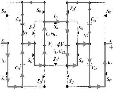
At the instant of +8Vi voltage level through connected load is provided by addition of supply voltage 4Vi with the capacitor voltage Ci2 and therefore, the capacitor is operated in discharging manner. Figure 4 shows the equivalent circuit of + 8Vi voltage level for proposed topology.
This mode of operation is achieved by turning on switches in the sequence of Si1, Si3, Si4, Si6, & Si7. In this mode of operation, the capacitors Ci1& Ci2' are used in charging condition by using turned ON of power switches Si2' & Si5' correspondingly. The Figure 5 represents the equivalent circuit for +10V level. When switching patterns are operated in the sequence of Si1'to Si5' are switched ON, while the two capacitors are connected serially with supply voltage. Whereas the charging capacitors are paralleled with input voltage of input voltage and 4Vi, correspondingly therefore, in this mode, the output load voltage is summing up with supply voltages, those are almost equal to the voltage level of +10Vi. In the same way, −10Vi is created by making turned ON the opposite switching pattern. Similarly, the remaining voltage levels also having various switching patterns. According to that only the SCMLI will operate and produce 21 level output voltage across the load.
Figure 4. Equivalent circuit of +8 voltage level
Figure 5. Equivalent circuit for +10 voltage level
These Pulse Width Modulation (PWM) techniques developed on the way to decrease the THD value of that load terminal voltage. Every variation on sinusoidal wave output load voltage are cause harmonic at load and this harmonic produce EMI, losses and pulsating torque occurs in electrical drives. However, the rising of switching frequency in PWM causes reduction of lower order harmonics by affecting the carrier switching frequency. The reference has maximum magnitude Ar and as well as frequency fr. The operating principle of multi carrier SPWM is that comparing of triangular carrier signal with sinusoidal reference wave. When carrier signal is more compared to reference then relevant switch is ON and when reference signal is more compared to carrier then relevant switch is OFF. Generally, MLIs, the amplitude value of modulating index is Ma and modulating frequency ratio Mf are shown in Eqns. (1) and (2).
$M_{a}=\frac{A_{r}}{(m-1) A_{c}}$ (1)
$M_{f}=\frac{f_{c}}{f_{r}}$ (2)
Here Ar and Ac are amplitude of reference and carrier wave in that order. Found fr and fc are frequencies of reference and as well as carrier wave correspondingly. Here modulation index value is taken as 0.98 for SCMLI for 14 power switches with different carrier signals.
3.1 Triangular multicarrier SPWM
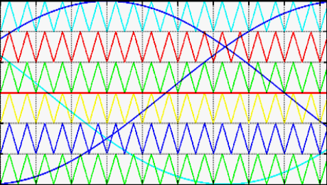
The multicarrier modulation technique is used for multilevel inverter and multilevel inverters completed with the usage of some triangular waves as a carrier signal and single sine wave as a reference wave for each and every phase and carrier implemented Sub-Harmonic PWM (SH-PWM) that followed m no. of level inverter, m-1 no. of carriers of similar frequency fc, identical magnitude Ac are liable such bands engage contiguously, which shows by usage of regular triangular carrier waves produce fewer harmonic distortions where output side of inverter. Now IPD technique is used. This IPD technique has better results than the other techniques. Figures 6 and 7 show the TMC SPWM technique of PD and IPD for the modulation index value of 0.8 and 1 respectively.
Figure 6. PD of TMC SPWM with modulation index value as 1
Figure 7. IPD of TMC SPWM with modulation index value as 0.8
4.1 Efficiency
The losses in the developed SCMLI structure is mostly intense on three main power losses, specifically losses during switching (Psw), losses during conduction (Pcon), and losses with capacitor ripples (Pripple). Then overall power loss (Ploss) of SCMLI is written as following:
$P_{\text {loss}}=P_{\text {sw}}+P_{\text {con}}+P_{\text {ripple}}$ (3)
The overall efficiency (η) of the developed inverter is given by the following Eq. (4):
$\eta=\frac{P_{O u t}}{P_{O u t}+P_{L o s s}}$ (4)
4.2 Switching losses
The most common losses of power semiconductor switch take place whereas the switch is operated in transition condition. Whenever the switching pattern is distorted in the position ON state to OFF state and vice versa, once the linear estimation among the switch voltage and the switch current throughout the transition period toff and ton is measured, the total energy losses are happened in the ith order power semiconductor switch is written as following expression:
$E i, o n=\int_{0}^{t_{o n}} V_{s w i}\left(1-\frac{t}{t_{o n}}\right) I_{i}\left(\frac{t}{t_{o n}}\right) d t=\frac{1}{6} V_{s w i} I_{i} t_{o n}$ (5)
$E i, o f f=\int_{0}^{t_{o f f}} I_{i}\left(1-\frac{t}{t_{o f f}}\right) V_{s w i}\left(\frac{t}{t_{o f f}}\right) d t=\frac{1}{6} V_{s w i} I_{i} t_{o f f}$ (6)
where, Ii and Ii' are represented the switching current parameters, behind ON state and ahead of OFF states. To identify the power energy switching losses from the fundamental time period of the ith order switch position, the amount of ON state conditions and OFF state transitions over a period can be evaluated. Hence, total energy power losses for one cycle period for the ith order switch position is expressed by the following equation:
$E_{i, s w}=\left(N_{O N, i} * E_{i, o n}\right)+\left(N_{o f f, i} * E_{i, o f f}\right)$ (7)
The total power switching losses of the ith order switch over a cycle are illustrated by the equation,
$\begin{array}{l}
P_{i, s w}=\frac{\left(N_{O N, i} * E_{i, o n}\right)+\left(N_{o f f, i} * E_{i, o f f}\right)}{T} \\
=\frac{1}{6 T} V_{s w i} I_{i}\left(N_{O N, i} t_{o n}\right)+\left(N_{o f f, i} * t_{o f f}\right)
\end{array}$ (8)
The overall switching losses in terms of power value can be proposed SCMLI inverter is calculated as following:
$\begin{array}{c}
P_{s w}=\sum_{i=1}^{14} P_{i, s w} \\
=\sum_{i=1}^{14}\left(N_{O N, i} * P_{i, o n}\right)+\left(N_{o f f, i} * P_{i, o f f}\right)
\end{array}$ (9)
4.3 Conduction losses
The total conduction losses in this developed inverter arrangement is measured by the each and every element’s internal resistance is considered for evaluation. From this investigation of the equivalent circuit the average power loss in conduction period in positive and as well as negative half cycles are same. The average power losses of conduction period for one full cycle are evaluated. During first positive voltage level, the total period is considered about the duration of (t2−t1) s in T (one full cycle). Therefore, the average loss of power during conduction for both first levels of load voltage given as following,
$P_{\text {ave1}}=\frac{2\left(t_{2}-t_{1}\right)}{T}\left(p_{1}+p_{1-}\right)$ (10)
The average power loss of the conduction period for remaining voltage levels are to be calculated based on Eq. (8). Thus, the average conduction losses for a cycle is expressed as following:
$P_{c o n}=\sum_{j=1}^{10} P_{a v e j}$ (11)
where, j=1, 2, 3,.…, 1.
4.4 Capacitor ripple losses
These are arisen because of voltage variation among that capacitor and its relevant feeding source. Considering capacitor Ck is associated with discharging operation on behalf of a greatest time period (tj+1−tj), subsequently highest voltage ripple of that consequent Ck is given in Eq. (12):
$\Delta v_{c k}=\frac{1}{c k} \int_{t i}^{t i+1} i_{c k}(t) d t$ (12)
iCk(t) is capacitor’s current during dis-charging. These currents are naturally similar to output terminal currents. Then capacitor ripple losses per one full cycle of capacitor Ck evaluated with following equation:
$P_{\text {ripck}}=\frac{1}{2 T} C_{k}\left(\Delta v_{c k}\right)^{2}$ (13)
The overall ripple losses for each and every capacitor are named as Ci1, Ci1', Ci2 & Ci2' for a full cycle is determined by following Eq. (13). Then entire capacitor ripple losses for one full cycle are given as following:
$P_{\text {ripple}}=P_{\text {ripcil}}+P_{\text {ripcil}^{\prime}}+P_{\text {ripcil}}+P_{\text {ripci2}^{\prime}}$ (14)
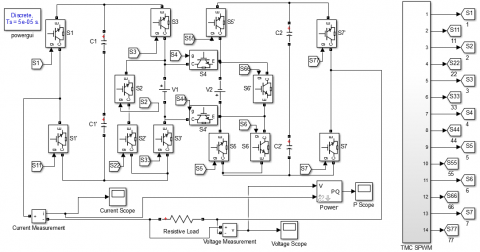
Figure 8. SIMULINK model
The Switched Capacitor Multilevel Inverter (SCMLI) model with triangular multi carrier SPWM is simulated in MATLAB software to demonstrate achievability of SPWM technique, which is shown in Figure 8. This proposed method gives about 96.02% of efficiency. Also reduces switching losses in lower value as 0.527 W, conduction losses as 4.69 W and capacitor ripple losses 0.0799 W.
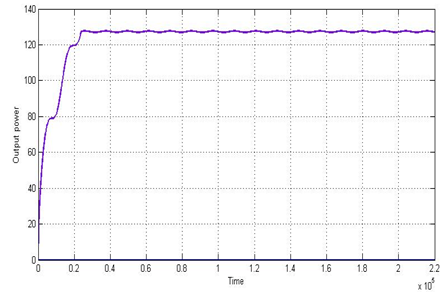
This simulation model considered IGBTs as power switches devices and the simulation results of SCMLI are obtained, when 50ohms resistive load is connected. Figure 8 shows simulated model of developed SCMLI and that designed and simulated using MATLAB/SIMULINK software. In this case, the amplitudes of the DC input power supplies are considered as 100 V & 400 V. By connecting an input DC voltage sources, the developed topology be able to create a high output voltage of 1000 V. The load across the SCMLI is 50ohms corresponding to that the output current of SCMLI is 45.4 A. The output power of developed SCMLI is obtained 127.66 W. Therefore, all the capacitors are set as 560μF when the primary switching method is implemented; switching losses are noticeably a smaller amount. From the calculation switching losses are obtained as 0.527 W, capacitors ripple losses as 0.0799 W and Conduction losses as 4.69 W. Then overall losses in developed SCMLI are 5.296 W. By the observation capacitor ripple loss and switching losses are smaller than conduction losses. With the output power and losses, the efficiency can be calculated using Eq. (2). This developed SCMLI produces output voltage about 1000V and it is shown in Figure 9 and Figure 10 using with & without filter. The output 21-level voltage waveform at load terminals to be shown in the Figure 11 as load current, which is 45.4A and output power as 127.66kW as shown in Figure 12. Table 1 gives obvious detail about input and output parameters of proposed system.
Figure 9. Voltage at load terminals without filter
Figure 10. Voltage at load terminals without filter
Figure 11. Load current waveform
Figure 12. Output power waveform
Table 1. Input and output parameters of SCMLI
|
Parameters |
Values |
|
Input Voltages – Asymmetric Voltage |
100 V, 400 V |
|
Output Voltage |
1000 V |
|
Output Current |
45.4 A |
|
Output Power |
127.66 kW |
|
THD of output voltage without filter |
8.34% |
|
Peak fundamental load voltage without filter |
858.5 V |
|
THD of output voltage with filter |
0.61% |
|
Peak fundamental load voltage with filter |
1002 V |
|
THD of output Current |
14.71% |
|
Switching losses |
0.527 W |
|
Conduction losses |
4.69 W |
|
Capacitor ripple losses |
0.0799 W |
|
Overall Efficiency |
96.02% |
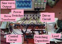
Figure 13. Hardware implementation
Figure 13 illustrates about the 21 level SCMLI hardware implantation. It consists of IGBT power switches, driver circuit, switching capacitor, drives transformer, resistive load and DSO. When DC input voltage is given by asymmetric DC voltage sources through 21 level SCMLI circuit, which converts sinusoidal voltage from filtering circuit. Figure 14 shows the FFT analysis of filtered output voltage, the THD value is reduced as 0.61%. While connecting a without filter circuit, it gives about 8.34% THD.
Figure 14. FFT analysis of a filtered output voltage
The Asymmetric DC Source configured SCMLI structure is developed and 21 output voltage levels across the load is carried out. Therefore, developed topology shows the potential to boosting of its source voltage and moreover, which provides considerably lesser losses than remaining topologies. It exhibits the efficiency of 96.02% and also compared with some topologies in several aspects like cost factor, no. of switching devices, no. of capacitors and etc. The proposed MLI is also applicable for high-voltage applications like industries as well as domestic purposes and RECS. Hence, it clearly justifies the developed SCMLI topology with Triangular Multi Carrier SPWM technique gives highly efficient than other topologies. It also has wide range of high voltage applications such as compensating devices in transmission, driving of electrical drives in industries and etc. Further this topology can be expended in different modulation technique to reduce power losses and improve overall efficiency.
[1] Roy, T., Bhattacharjee, B., Sadhu, P.K., Dasgupta, A., Mohapatra, S. (2018). Step-up switched capacitor multilevel inverter with a cascaded structure in asymmetric DC source configuration. Journal of Power Electronics, 18(4): 1051-1066. https://doi.org/10.6113/JPE.2018.18.4.1051
[2] Samanbakhsh, R., Taheri, R. (2016). Reduction of power electronic components in multilevel converters using new switched capacitor-diode structure. IEEE Transaction on Industrial Electronics, 63(11): 7204-7214. https://doi.org/10.1109/TIE.2016.2569059
[3] Gupta, K.K., Jain, S. (2016). Multilevel inverter topologies with reduced device count: A review. IEEE Transaction on Power Electronics, 31(1): 135-151. https://doi.org/10.1109/TPEL.2015.2405012
[4] Hinago, Y., Koizumi, H. (2010). A single-phase multilevel inverter using switched series/parallel DC voltage sources. IEEE Transaction on Industrial Electronics, 57(8): 2643-2650. https://doi.org/10.1109/TIE.2009.2030204
[5] Sano, K., Fujita, H. (2008). Voltage-balancing circuit based on a resonant switched-capacitor converter for multilevel inverters. IEEE Transactions on Industry Applications, 44(6): 1768-1776. https://doi.org/10.1109/TIA.2008.2006291
[6] Babaei, E. (2008). A cascade multilevel converter topology with reduced number of switches. IEEE Transaction on Power Electronics, 23(6): 2657-2664. https://doi.org/10.1109/TPEL.2008.2005192
[7] Rodriguez, J., Wu, B., Bernet, S., Pontt, J., Kouro, S. (2007). Multilevel voltage source converter topologies for industrial medium voltage drives. IEEE Transaction on Industrial Electronics, 54(6): 2930-2945. https://doi.org/10.1109/TIE.2007.907044
[8] Ceglia, G., Guzman, V., Sanchez, C., Ibanez, F., Walter, J., Gimenez, M.I. (2006). A new simplified multilevel inverter topology for DC-AC conversion. IEEE Transaction on Power Electronics, 21(5): 1311-1319. https://doi.org/10.1109/TPEL.2006.880303
[9] Rodriguez, J., Lai, J.S., Peng, F.Z. (2002). Multilevel inverters: A survey of topologies, controls, and applications. IEEE Transaction on Power Electronics, 49(4): 724-738. https://doi.org/10.1109/TIE.2002.801052
[10] Mak, O.C., Ioinovici, A. (1998). Switched-capacitor inverter with high power density and enhanced regulation capability. IEEE Transactions on Circuits and Systems I: Fundamental Theory and Applications, 45(4): 336-347. https://doi.org/10.1109/81.669056
[11] Chandrasekaran, G., Periyasamy, S., Rajamanickam, K.P. (2020). Minimization of test time in system-on-chip using artificial intelligence based test scheduling techniques. Neural Computing and Applications, 32(9): 5303-5312. https://doi.org/10.1007/s00521-019-04039-6
[12] Chandrasekaran, G., Periyasamy, S., Karthikeyan, P.R. (2019). Test scheduling for system on chip using modified firefly and modified ABC algorithms. SN Applied Sciences, 1(9): 1079. https://doi.org/10.1007/s42452-019-1116-x
[13] Chandrasekaran, G., Kumarasamy, V., Chinraj, G. (2019). Test scheduling of core based system-on-chip using modified ant colony optimization. Journal Européen des Systèmes Automatisés, 52(6): 599-605. https://doi.org/10.18280/jesa.520607
[14] Parimalasundar, E., Suthanthira Vanitha, N. (2015). Identification of open-switch and short-switch failure of multilevel inverters through DWT and ANN approach using LabVIEW. Journal of Electrical Engineering and Technology, 10(6): 2277-2287. http://dx.doi.org/10.5370/JEET.2015.10.6.2277