Fouzi Haddad* | Mustapha Hatti | Khadidja Rahmoun | Katir Ziouche
© 2022 IIETA. This article is published by IIETA and is licensed under the CC BY 4.0 license (http://creativecommons.org/licenses/by/4.0/).
OPEN ACCESS
There are many effective technologies that have been developed in the field of renewable energy. In this context, this study covers a selective coating used in the photo-thermal conversion on macro-scale devices. The objective of this work is to optimize a silicon-based paint layer for solar application in the low temperature range (T<80℃) where the optimization thickness is found 21 µm. In order to apply the optimization layer (21 µm) in the solar devices that work in the medium temperature range (80℃<T<200℃), we propose to deposit a thin film of indium oxide using an ultrasonic spray chemical vapor deposition USCVD process to obtain finally a bilayer structure (silicon-based paint Thickness-Insensitive Selective Solar TISS / In2O3). The obtained bilayer structure was tested and characterized using spectroscopy of UV-VIS and IR, the last one was used in two modes: specular and diffuse reflection. The structural properties were investigated using the X-rays diffraction (XRD) and the morphological character was analyzed using Scanning Electron Microscope (SEM). In addition, the global results denote that the deposition of In2O3 layer improves the reflection capacity of the optimization layer (21 µm) from 8 to 11 in the NIR range.
photo-thermal conversion, solar paints, solar absorber, solar water heater, spectral selectivity, selective surfaces, thin layers
The energy transition has become a big challenge to any government because of the dramatic climate change that occurred during the few last decades. The energy crisis in 1973 has promoted the renewable energies as an alternative to fossil ones [1]. Furthermore, this interest has become more pronounced with the emergence of laws and charters bound to protect the environment due to the KYOTO protocol since 1997. After that, an international agreement on climate change has been signed in Paris in April 2016. Since solar energy is the most widespread source of renewable energy, a special attention is given to this source. Typically, solar energy can be converted to a photon-electron or photo-thermal energy [2]. When solar energy is converted to thermal energy, the use of selective surfaces is mandatory in order to compete with the other way of conversion which is electrical [3]. There are several techniques to prepare selective surfaces: intrinsic material, interferential filter, absorber-reflector implements, diffusion in volume effect, texture effect, and selective paints [4, 5]. The first attempt in the development of selective paints were reported by Gunde et al. [6]. It has been the subject of research into less expensive alternative materials to chromium, which used as a coating for solar thermal absorbers [6]. Basically, two types of paints were developed, one is sensitive to thickness (TSSS: Thickness-Sensitive Selective Solar) and the other is insensitive to thickness (TISS: Thickness-Insensitive Selective Solar) [7]. Thickness–insensitive paint coating was developed with urethane, acrylic, and silicone binders. This type of coating combines the selective coatings currently developed and aluminum flake to provide a low emitting substrate, by varying the ratio of paint to flake, where the selective properties: α=0.90 and ε=0.31 were achieved [8]. After these results, the interest in such works has been increased to obtain more effective selective paints. In this context, there are several investigations that examined the effect of Pigment Volume Concentration (PVC) on the rendment of the photo-thermal conversion [9-11].
In this work, we purpose a slightly different approach, from a PVC; to optimize the thick of our samples, we realized different thicknesses of the micrometric order using the spin coating method. In addition, we report in details, for the first time, an experimental investigation, where the main goal is to increase the absorption of solar radiation as possible, at the same time limiting the loss of radioactive heat from the absorber surface and this feature is released through deposition of In2O3 layer, where In2O3 layer exhibit an attractive reflectance property in IR game.
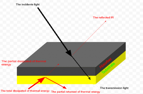
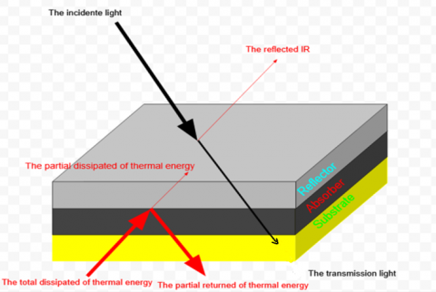
When a beam of light falls on a sample, that has a substrate coated with an absorbent paint that contains a dispersed pigment inside that paint. Reflection, transmission and absorption can occur. If the paint is optically deep enough, the light transmitted is negligible [12]. There are two types of reflection: specular reflection and diffuse reflection. For smooth surfaces the specular reflection is significant, while the diffuse reflection occurs in rough surfaces where the incident radiation on the surface will be reflected again by the grain boundaries of the particles (scattered pigments). The most important parameter in diffuse reflection is the particle size. If the particle size decreases the number of reflections at grain joints increases. As a result, the depth of penetration of the incident solar radiation decreases, resulting in a decrease in absorption and an increase in reflectance [13]. In our study, a selective paint for a solar collector absorber of low and medium temperatures that ensures both a good absorbance of visible solar radiation and a good reflection for infrared radiation that is investigated. Infrared reflective pigments were used in the manufacturing of these paints such as pure metals like Al, Ag and Cu, and silicon powder. These pigments will be dispersed in a silicon-based paint to apply it on the substrate of the absorber in order to make it selective to solar radiation [14]. Solar radiation balance of a solar absorber, having its rear and side faces perfectly insulated and exposed to solar radiations, reaches an equilibrium temperature such that the power received is equal to the power lost. The conversion yield is given by [15]:
$\eta_{c}=\alpha\left[1-\frac{\varepsilon}{\alpha} \frac{\sigma\left(T^{4}-T_{a}^{4}\right)}{H}\right]$ (1)
Considering Eq. (1), the yield can be increased by increasing the a/e ratio.
In general, in the literature, the absorption coefficient is taken such as the incidence angle θ is equal to 0 (normal to the surface), then we have [16]:
$\alpha=\frac{\int_{0.3}^{2.5} \alpha_{\lambda} I_{s o l}(\lambda) d \lambda}{\int_{0.3}^{2.5} I_{s o l}(\lambda) d \lambda}$ (2)
The global emissivity coefficient is given for an incidence angle equal to 0 by:
$\varepsilon=\frac{\int_{2.5}^{27} \varepsilon_{\lambda}(T) I_{p}(\lambda) d \lambda}{\int_{2.5}^{27} I_{p}(\lambda) d \lambda}$ (3)
The reflection coefficient R can be expressed as function of α and ε considering the Kirchhoff’s law, for specific wavelength l, as follow [12]:
$\alpha_{\lambda}=\varepsilon_{\lambda}=1-R_{\lambda}$ (4)
3.1 Substrate preparation
Among the wide varieties of techniques for depositing selective layers, we chose a spin coated process that is well mastered and less expensive, this machine exists in the IEMN laboratory. In this paper, we used substrate already prepared from a silicon wafer with a thin gold layer of 200 nm deposited onto it by evaporation technique (with PLASSYS MEB 550 S), as shown in Figure 1 (that can be considered like a perfect mirror).
The choice of the gold substrate is conditioned by its good reflectivity allowing it to be a super reference material for rigorous spectroscopic characterization on the one hand. On the other hand, the adhesion of the resin-based liquid solution on the substrate must be sufficiently strong. In addition, the chemical composition of the substrate must not lead to contamination of the deposited thin film by diffusion of chemical species during annealing. The silicon/gold wafer was formed as substrate squares with about 2.5 cm; they were rinsed with ethanol for 10 min and then dried under a stream of nitrogen.
Figure 1. Silicon/gold wafer prepared from a silicon wafer with a thin gold layer of 200 nm deposited onto it by evaporation technique
3.2 Deposit process
The silicon based paint was prepared in the laboratory of National Paint Company (Lakhdaria, Algeria). To deposit this paint we used spin coating technique where the centrifugation process involves spreading a drop of the silicon based paint (gelled) onto a rotating substrate. This technique is generally carried out in four main steps: 1. depositing the solution on the substrate, 2. Spin up (accelerated rotation), 3. Spin off (uniform rotation), 4. Evaporation (uniform speed). The uniform rotational speeds and the rotational time of the substrate are summarized in the table.
The thicknesses of the four substrates were measured with a profilometer with a sensitivity of few nanometers; the results obtained are shown in Table 1.
Relative to the sample number 4, the operation was repeated 4 times under the same conditions. All samples were annealed at a temperature of 80°C for 10 min, and the obtained result is clarified in Figure 2.
Figure 2. Schematic of the deposition silicon based paint on gold substrate (low temperature solar absorber applications)
Table 1. Experimental factors of spin coating process
|
|
Sample 1 |
Sample 2 |
Sample 3 |
Sample 4 |
|
Conditions of the 1st stage of deposition |
V1=500 rpm Rise=2 s Time=60 s |
V1=500 rpm Rise=2 s Time=60 s |
V1=500 rpm Rise=2 s Time=60 s |
V1=500 rpm Rise=2 s Time=60 s |
|
Conditions for the 2nd deposition stage |
V1=5000 rpm Rise=4 s Time=60 s |
V1=3500 rpm Rise=4 s Time=60 s |
V1= 2000 rpm Rise=4 s Time=60 s |
V1=2000 rpm Rise=4 s Time=60 s |
|
Thickness |
10 µm |
14 µm |
21 µm |
42 µm |
Table 2. Experimental conditions of ultrasonic Spray CVD process
|
Deposition time (min) |
Solution flow rate (ml/h) |
Temperature (°c) |
Distance spray nozzle–substrate (cm) |
Morality (mole/h) |
|
4 |
40 |
250 |
5 |
0.1 |
Figure 3. Schematic of the deposition of bilayer structure In2O3/ silicon base paint on gold substrate (medium temperature solar absorber applications)
For solar applications in the medium temperature range, we deposited nanostructured thin layers of indium oxide on our samples using an USCVD process (see Figure 3). Indium oxide thin films were prepared by spraying a solution containing a 0.1M of indium chloride InCl3 (with purity of 99.999% provided by sigma Aldrich) in absolute volume of ethanol (C2H5OOH) as a solvent (provided by sigma Aldrich). Furthermore, Table 2 summarizes the experimental conditions.
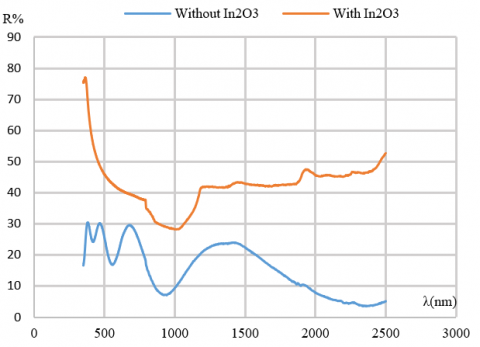
Figure 4 shows the reflectance variation for a silicon substrate (piece of wafer) and the same substrate is coated with a 300 nm layer of In203. This justifies our choice of ln203 as a good reflector in the NIR band.
Figure 4. Reflectance of a silicon substrate (peace of wafer) and the same substrate coated with 300 nm of In203 layer
3.3 Characterization
There are several techniques of characterization were used to investigate properties of the obtained samples such as:
All the samples were characterized by spectrometer of the brand CARY 500 DE VARIAN equipped with an integrating sphere; the spectrum range extends from 175 nm up to 3300 nm (UV- VIS - NIR), in a first step. To characterize a behavior of these samples in the MIR domain they were passed through a brand spectrometer ELMER PARKIN 2000 (FTIR) in the spectrum range 1 µm up to 27 µm. All spectroscopic characterization operations were in reflection mode.
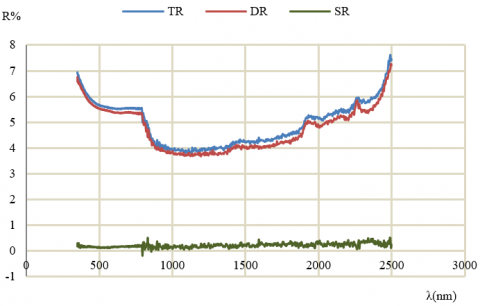
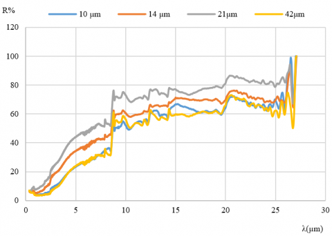
The Figure 5 shows practically zero variation in the specular reflectance for all the thicknesses of silicon based paint deposited over the entire UV-VIS-NIR spectrum. Also, there is a low diffuse reflectance in the UV-VIS range with an appreciable increase in the NIR as a function of the deposited layer’s thickness. In addition, the maximum value of the diffuse reflectance is reached at a thickness of 21 μm, after this value the increase in thickness only decreases the diffuse reflection in the near infrared (NIR) region, this reduction is due to the promotion of multiple reflections inside the resin layer. The explanation for this increase comes down to the concentration of the silicone pigment inside the layer. In conclusion, 21 µm is found to be the optimum thickness of this resin.
The diffuse reflection increases as a function of the thickness in the NIR band which proves the role of the dispersed pigments in the NIR band inside the silicon based paint and it reaches the maximum at a thickness 21 µm then it decreases as mentioned in Figure 6 (a). The physical explanation for this decrease is due to multiple reflections. The absorption and thermal emissivity factors were calculated from the curves Figure 6 (b) and the equations witch link these as a function of reflectance. The obtained results are given in Table 3.
(a) 10 mm
(b) 14 mm
(c) 21 mm
(d) 42 mm
Figure 5. Total reflectance (TR), diffuse reflectance (DR)and specular reflectance (SR) of samples as a function of thickness of a layer of paint on a gold substrate
(a)
(b)
Figure 6. Reflectance as a function of wavelength for different paint thicknesses on a gold substrate, a (350-2500) nm and b (2.5-27) µm
Table 3. The calculated thermal emissivity factors
|
Thickness (µm) |
α |
ε |
α/ε |
|
10 |
0.85 |
0.23 |
3.70 |
|
14 |
0.82 |
0.20 |
4.1 |
|
21 |
0.80 |
0.15 |
5.33 |
|
42 |
0.83 |
0.21 |
3.95 |
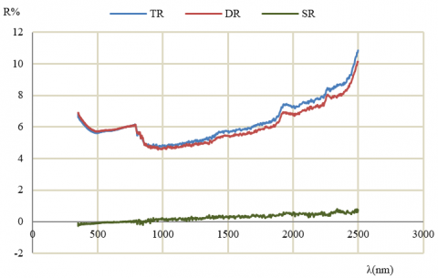
The deposition of In2O3 layer with thickness of 300 nm on the silicon based paint (21 µm) / Gold substrate shows a significant increase in reflectance in the NIR band with a slight decrease in absorption in the VIS band. This increase is about 8% after calculation based on the data obtained in Figure 7 a, and b. These figures show the aptitude of In2O3 to reflect the infrared IR.
The XRD pattern of bilayer is shown in Figure 8. We note that the majority of diffraction peaks are correspond to the aluminum with cubic system and Fm3m space group and constant cell is 4.0494 (Å) as reported in card number (00-004-0787), aluminum is used in this paint as a pigment. Furthermore, there are two peaks of the orthorhombic SiO2 phase (card 00-001-0378), these peaks located at 25.27° and 27.12° relative to the (050) and (015) plans, respectively. The insert figure highlights the relatively weak peaks of cubic In2O3 phase, the first peak located at 30.35° is due to the plan (222) and the second peak cited at 35.77° denotes the (400) plan (card 00-006-0416), which confirm the presence of indium oxide phase. Moreover, this result goes in harmony with objective of this investigation.
We present a series of 2D scanning electron microscope images, showing the surfaces of the two deposits. Image (a) and (b) show the first deposit of the silicon-based paint on a gold substrate and pictures (c) and (d) illustrate the deposit of the In203 layer on the first deposit.
Figure 7. The Reflectance of 300 nm layer of In203 deposited on silicon based paint / Gold substrate
Figure 8. XRD spectrum of silicon-based paint/In2O3 bilayer
In Figure 9 (a) and (b) we can see the uniformity of distribution of Aluminum pigments within the silicon based paint and also give us an idea of the size of these pigments which varies between 1 and 5 microns which has produced an apparent increase in reflectance in NIR.
In Figure 9 (c), contrasts are shown allowing a homogeneous surface view of In2O3 except for some cracks due to the high temperature of the deposition process. The presence of clusters of beads in the In2O3 layer proves its good reflectance of radiation in the NIR band as shown in Figure 9 (d).
(a)
(b)
(c)
(d)
Figure 9. SEM image shows the surfaces of the two deposits. Image (a) and (b) display the first deposit of the silicon-based paint on a gold substrate. Image (c) and (d) illustrate In203 layer on the first deposit
Selective surfaces are coated surfaces where it exhibits a maximum absorbance for solar radiation and minimum thermal emissivity for thermal radiation. The objective of this study is to offer a selective surface at an acceptable cost for solar thermal applications for medium temperatures between 80°C -200°C. To release this objective, we suggest a new approach, where we started from synthezing a conventional bilayer TISS using spin-coating technique with thicknesses of the order: 10 to 45 µm. The spectroscopic characterizations of the silicon-based resin showed zero specular reflection for all thicknesses. However, the layer that has thicknesses of 21 µm appears a critical value of specular reflection. The obtained samples from first phase can be applied in the low temperature range (T<60°C). In addition, the USCVD technique was applied to deposit thin layer of In2O3 to obtain TISS / In2O3 that has the optimum thickness of 21 microns which gives maximum reflection in the NIR. The deposition of In2O3 improves the reflection capacity from 8 to 11 in the NIR range, which makes final product “TISS / In2O3” a good candidate to use it in the photo-thermal conversion on macro-scale devices that work in the medium temperatures range (100°C-250°C)
|
I |
direct normal irradiance, W.m-² |
|
|
H |
incident power, W.m-² |
|
|
T |
temperature, K |
|
|
R |
reflectance |
|
|
Greek symbols |
||
|
$\alpha$ |
Absorption coefficient |
|
|
ε |
thermal emissivity coefficient |
|
|
θ |
Incidence angle, rad |
|
|
η |
yield |
|
|
λ |
Wave length, m |
|
|
σ |
Stephan Boltzman constant, w.m-2.k-4 |
|
|
Subscripts |
||
|
a |
ambient |
|
|
p |
plank black body |
|
|
sol |
solar |
|
[1] Aissaoui1, F., Benmachiche, A.H., Brima, A., Belloufi, Y., Belkhiri, M. (2017). Numerical study on thermal performance of a solar air collector with fins and baffles attached over the absorber plate. International Journal of Heat and Technology, 35(2): 0392-8764. https://doi.org/10.18280/ijht.350209
[2] Daranfed, W., Guermat, N., Mirouh, K. (2020). Experimental study of precursor concentration the Co3O4 thin films used as solar absorbers. International Journal of Heat and Technology, 44(20): 121-126. https://doi.org/10.18280/acsm.440207
[3] Ardente, F., Beccali, G., Cellura, M., Brano, V.L. (2005). Life cycle assessment of a solar thermal collector: Sensitivity analysis, energy and environmental balances. Renewable Energy, 30: 109-130. http://dx.doi.org/10.1016/j.renene.2004.05.006
[4] Pérez, I.H. (2016). Multilayer solar selective coatings for high temperature solar applications: From concept to design. Ph.D. Department of inorganic chemistry university of Seville, Spain.
[5] Chiua, J.S., Younga, W.B. (2018). Theoretical approach to simulate efficient selective solar absorbers with micro or nano structured arrays. Materials Research, 21(3): e20171026. http://dx.doi.org/10.1590/1980-5373-MR-2017-1026
[6] Gunde, M.K., Orel, Z.C. (2000). Absorption and scattering of light by pigment particles in solar-absorbing paints. Applied Optics, 39(4): 622-628. https://doi.org/10.1364/AO.39.000622
[7] Alshamaileh, E. (2010). Testing of new solar coating for solar water heating applications. Solar Energy, 84(240): 1637-1643. https://doi.org/10.1016/j.solener.2010.06.003
[8] Mckelvey, W.D., Zimmer, P.B., Lin, R.J. (1979). Solar selective paint coating development final report, Honeywell Inc. Systems and Research Center and Avionics Division Minneapolis, Minnesota. USA.DOE/CS/34287-T1. https://www.osti.gov/biblio/5140021.
[9] Malshe, V.C., Bendiganavale, A.K. (2008). Infrared reflective inorganic pigments. Recent Patents on Chemical Engineering Journal, 1(1): 67-79. https://doi.org/10.1016/j.solmat.2003.06.001
[10] Gunde, M.K., Lozar, J.K., Orel, Z.C. (1996). Optimum thickness determination to maximize the spectral selectivity of black pigmented coatings for solar collectors. Thin Solid Films Journal, 277: 185-191. https://doi.org/10.1016/0040-6090(95)08023-6
[11] Gunde, M.K., Orel, Z.C., Hutchins, M.G. (2003). The influence of paint dispersion parameters on the spectral selectivity of black-pigmented coatings. Solar Energy Materials and Solar Cells Journal, 80: 239-245. https://doi.org/10.1016/j.solmat.2003.06.001
[12] Orel, B., Spreizer, H., Perse, L.S., Fir, M., Vuk, A.S., Merlini, D, Voldan, M., Kohl M. (2007). Silicone-based thickness insensitive spectrally selective (TISS) paints as selective paint coatings for coloured solar absorbers (part 1). Solar Energy Materials and Solar Cells Journal, 91: 93-107. https://doi.org/10.1016/j.solmat.2006.07.013
[13] Duffie, J.A., Beckman, W.A. (2005). Solar Engineering of Thermal Processes. 3rd Ed, John Wiley and Sons, New York, USA.
[14] Fang, V., Kenedy, J.V., Futter, J., Manning, J. (2013). A review of infrared reflectance properties of metal oxide nanostructures. GNS Science Report.
[15] Haddad, F., Chikouche, A., Laour, A. (2011). Simulation of the opti-physical parameters of selectives surfaces of absorber by the FDTD method applied to solar water heater. Energy Procedia, 6: 413-421. https://doi.org/10.1016/j.egypro.2011.05.048
[16] Roro, K.T., Tile, N., Yalisi, B., De Gama, M., Wittes, T., Roberts, T., Forbes, A. (2011). Selective solar absorber coating research at the CSIR (South Africa). Solar thermal applications (STH). World renewable energy congress 2011-Sweden 8-13 may Linkoping, Sweden. http://hdl.handle.net/10204/5310.