Challa Padma* | Palapati Jagadamba | Patil Ramana Reddy
© 2022 IIETA. This article is published by IIETA and is licensed under the CC BY 4.0 license (http://creativecommons.org/licenses/by/4.0/).
OPEN ACCESS
Presently Fourth generation and other wireless systems are focused area for the research and development in the communication field. Fast Fourier Transform (FFT) & Inverse FFT (IFFT) are required for Orthogonal frequency division multiplexing in the integral part of modulation/demodulation modules that occupies more area and power. This paper presents low power and area efficient Cached memory for Fast Fourier Transform (FFT) processor using floating point arithmetic for OFDM application. To store computational permutations each butterfly unit needs one memory. So if considering higher radix of FFT processor, memory requirement increases, it yields to more power consumption and more density occupancy. In this proposed cached 64 point radix 2^6 SDF architecture for reducing the arithmetic hardware complexity of complex multipliers and complex adders present in butterfly structure to obtain low power and less memory requirement. The proposed system is synthesized by using CADENCE RTL COMPLIER and is implemented in ENCOUNTER RTL TO GDSII SYSTEM” using 90nm CMOS technology with a supply voltage of 1V. Synthesis results shows that the proposed design is efficient in terms of gate count, area and power consumption.
Vedic multiplier, single path delay feedback (SDF), Kogge Stone Adder with mux, orthogonal frequency division multiplexing, cache memory
In OFDM systems, modulation and demodulation operations are carried out by using “Inverse Fast Fourier Transformation (IFFT) and Fast Fourier Transformation (FFT)”. In digital signal processing system these 2 are main blocks in an OFDM system. There are various types of FFT architectures used in OFDM systems to reduce the complexity computation. A small radix has simple butterfly structure, but numbers of twiddle factors are high if the size of FFT is large. Higher radix has less number of twiddle factors but butterfly structure is complex and speed of the FFT processor is also reduced. To obtain less number of twiddle factors and simple butterfly structure is possible through radix 2^K architectures are most widely used in present FFT processor implementation. The speed of the FFT processor is purely based on storage of twiddle factors, which is possible through cache memory. In conventional FFT architectures data and identical twiddle factor are stored in processor memory itself. If the number of points of FFT increased the size of the memory is also increased and simultaneously the speed of the FFT processor is reduced. In this research we concentrate on memory utilization for that here proposed modified cached FFT architecture using radix 2^6 single path delay feedback (SDF).
The Fast Fourier transform (FFT) is essential component in OFDM communication systems. During the last3 decades, several FFT architectures have been introduced, first completely [1] executed in 1999, the cached-FFT algorithm are used to construct custom FFT processors: A 512-point [2] 2D FFT chip, and [3] a programmable 64-2048 point FFT chip. They can be categorizing into 3 types- the parallel, pipeline and the memory architecture. The parallel and pipeline architectures consist huge butterfly processing elements to get good performance but occupies [4, 5] wide area when compared to memory architecture. The advantage of shared memory architecture employs only 1 butterfly processing elements area efficiency [6]. The trade-off between speed and hardware overhead is the main criterion for architecture selection. The difficulty of implementing FFT/IFFT is reduced due to VLSI advanced technologies. A special data calibration technique is accomplished by including empty records among data blocks. Due to the calibration, the samples processed in one FFT butterfly have different [7] memory addresses that reduces memory conflicts. Implementation of reconfigurable FFT processor with [8] complex multipliers containing 3 multiplications formatted on Radix 2, Radix 4 & Radix 8, algorithms consume more power. Existing approaches uses FFT/ IFFT processor, that offers adequate throughput values, but the cost is high due to Fu and Ampadu [9] increased hardware complexity. With cached memory FFT processor produces wide efficiency of a MIMO system, but reduction in throughput [10]. 64 and 128 point FFT/IFFT processor is implemented [11, 12] to meet IEEE 802.11n which contribute various throughput values for simultaneous data sequences. Due to increase in more number of points the complexity and cost of the system increases. FFT processor design based on pipeline will achieves larger data throughput by adding several “processing elements (PE)” and data paths was considered [13, 14], that results in large power consumption. In Long-length [15] FFT processor consists of higher radix-23 FFT algorithm and Memory-based architecture is implemented without considering data throughput has a large issue. Single-memory, dual-memory, array type and pipelined architecture is discussed [16] for implementations of FFT processors with different structures. Typical Existing FFT algorithms are proposed to reduce the number of adders and multipliers. But, ignored the memory functions usually. Hidden memory functions consume half of the power in the total FFT calculations [17]. The reconfigurable FFT/inverse FFT (IFFT) processor with single-chip is presented [18-20], gives a result to dedicated ASICs and software programmable DSPs. Energy-efficiency can be determined by containing “Application Specific Instruction Set Processors (ASIPs)” [21, 22] and it contains large area. The design flow depends on the Architecture Description Language (ADL) LISA is explained [23] and a framework for automated ASIP implementation is explained [24]. Allow power and area efficient 16-bit word-width 64-point radix-2^2 and radix-2^3 pipelined FFT architectures for an OFDM based IEEE 802.11a Wireless Local Area Network (WLAN) baseband is presented [25]. The designs are developed from “radix-2^K algorithm and used Single-Path Delay Feedback (SDF) [26, 27] architecture for hardware implementation”. The authors are mainly focused to overcome the complex multipliers and read-only memory (ROM) are used for internal storage of twiddle factor coefficients, proposed 64-point FFT consists a “Canonical Signed Digit (CSD) complex constant multiplier using adders, multiplexers and shifters” presented [28]. However, the above discussed results are still not enough in day to day needs like transmission speed and area. This paper discusses the aforementioned problems by decreasing the effective area and power with increase in throughput.
This paper is arranged as follows. In Section 2, we present a brief introduction of memory requirements. Section 3 discusses related cache memory overview. In section 4, discuss about the binary floating point Vedic multiplier using KSA (Mux) and section 5 deals with implementation of FFT. Section 6 discusses about the results and finally conclusion and future work are dealt in section 7.
More stringent is speed draw backs; with the memory access time. For an in-place N-point radix-r FFT contains a one memory bank, “2NlogrN” read or write RAM operations are required. In the present case, for a radix-2 existing FFT this results in a memory access time of approximately five nano seconds, which is quite complex to achieve. Memory usage versus speed is one of the major trade-off seen in algorithm implementation. The FFT is a one of the main core computational component in portable signal processing applications. However, a few applications can afford due to a more memory space for implementing FFTs. While memory utilization is an important for hardware implementation, memory accesses is also an account for a significant part in computation time. “This is attributed to cache misses, swapping and other paging effects”. These effects are wide prominent when calculating higher order FFTs (typically over 4K points). These observations are considered us to include memory utilization is a one of the yardsticks in judging the performance of the several FFT algorithms.
The cached-memory architecture has two major advantages are listed below.
1 High Speed—smaller memories are faster than large memories
2 High Energy Efficiency— smaller memories require lower energy
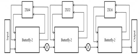
While using cached-memory architecture, achieved the major gains as speed and energy efficiency. In this data pre-fetching is possible, due to the proposed design is almost like that of single memory architecture except the cache between the FFT processor and processor memory. Figure 1 shows the overall block diagram of proposed work. It is designed that data caches increase the effective bandwidth to a memory— because the memory access pattern exhibits enough locality. The “FFT algorithm is deterministic, cache tags are unnecessary, and proper cache operation is achieved through a fixed, predetermined, cache address mapping”. Since the flow of knowledge of data is data independent, data can also be pre-fetched from processor memory before they’re needed.
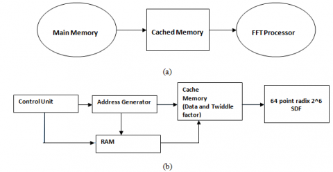
Figure 1. Block diagram of modified 64 point cached FFT architecture
In convention FFT architecture data and identical twiddle factors are stored in processor memory itself. If the number points of a FFT is increased, the size of the memory is also increased, and simultaneously the speed of the processor is reduced. To overcome this problem, data and identical twiddle factors are stored in cache memory. Other than the data and identical twiddle factors, address generating circuit and access control unit are stored in the processor memory. The size of the cache memory is very less compared with processor memory and the speed of the cache memory is very fast compared with main memory. Proposed modified Cached FFT architecture consists of two main blocks, namely Processor memory and cached memory. Processor memory consists of three major parts namely address generator, RAM, and control unit. Conventionally data is stored in processor memory (Main memory).
Address generating circuit provides address to the processor memory and cache memory. The Address Generation Unit (AGU) controls the generation of addresses for reading and writing the memory contents to and from the RAM and Cache Memory. The address generator finds a grouping of the memory accesses such some of the complete FFT are often calculated using less than N words of memory. The Address Generator Unit provides signals that control writes to memory as well as which memory bank is read. All data busses provide complex data transfer (double bit widths to accommodate both real and imaginary values). Each data has 32 bit width since data is a floating point representation. The read from one RAM block, and is transfers to the cache memory for speedy operation with FFT processor unit. The result is written back to RAM memory through cache memory.
The control logic unit performs FFT and IFFT. Three major functions are performed by the Control Logic Unit (CLU) which is given below:
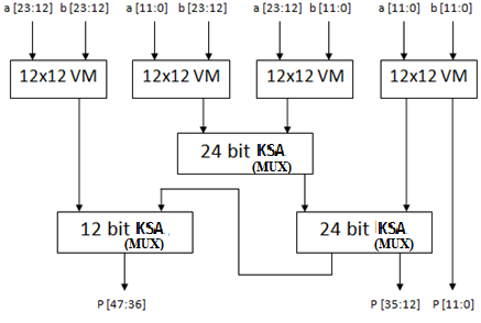
In single precision binary floating point architecture the mantissa part is computed by using 24X24 Vedic multiplier based on Urdhva-Tiryakbhyam sutra is efficient in multiplication algorithm as compared to conventional process as shown in Figure 2. Urdhva-Tiryakbhyam means vertically and crosswise sutra.
Figure 2. Block diagram of proposed 24X24 Vedic multiplier
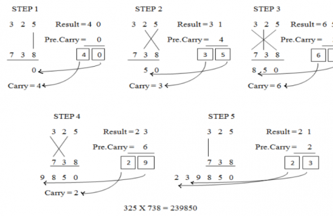
Figure 3. Multiplication of two decimal numbers by Urdhva-Tiryakbhyam
To illustrate this multiplication scheme, let us consider the multiplication of two decimal numbers (325 * 738). Line diagram for the multiplication is shown in Figure 3. The digits on the both sides of the line are multiplied and added with the carry from the previous step. This generates one of the bits of the result and a carry. This carry is added in the next step and hence the process goes on. If more than one line is there in one step, all the results are added to the previous carry. In each step, least significant bit acts as the result bit and all other bits act as carry for the next step. Initially the carry is taken to be zero.
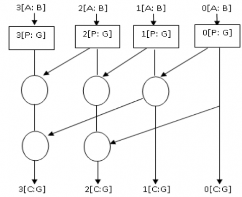
Figure 4. Basic block diagram of Kogge Stone Adder
Kogge stone adder is one of the fastest adders as shown in Figure 4, in this the addition operation is carried out in 3 steps, such as pre-processing, carry generation and post processing unit based on Eqns. (1)-(4).
$\mathrm{P}=\mathrm{A}_{i} \,\, \mathrm{X}-\mathrm{OR}\,\, \mathrm{B}_{i}$ (1)
$\mathrm{G}=\mathrm{A}$ AND B (2)
$C_{i}=G_{i}$ (3)
$S_{i}=P_{i} \,\, X-O R \,\, C_{i+1}$ (4)
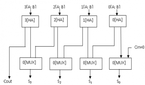
Figure 5. Proposed KSA by using MUX
In Kogge stone adder X-OR can be replaced by Mux as shown in Figure 5, which gives true and complement value at a time.
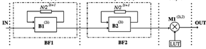
The single path delay feedback basic radix-2 and radix-2^2 architectures are shown in Figures 6 and 7. These architectures are mainly used to reduce arithmetic hardware complexity. In this proposed radix 2^6 SDF architecture requires 6 complex multipliers, 8 constant multipliers and 2 complex adders, these architectures reduce the overall twiddle factors required to compare radix 2^3, radix 2^4 and radix 2^5, butterfly structure multiplication is carried out by using Vedic multiplier using Urdhva-Tiryakbhyam. Further optimize the memory the proposed FFT processor is implemented on cached FFT architecture. The processor memory and cache memory are mainly utilized to decrease the power consumption since they operate at different frequencies.
Figure 6. Basic 64 point radix 2 SDF architecture
Figure 7. Radix 2^2 SDF architecture
Floating-point arithmetic is an efficient technique for the implementation in a variety of Digital Signal Processing (DSP) applications; because without worrying about numerical issues it allows the designer and user to focusmore on the algorithms and architecture. The FFT is one of the main popular transform algorithms in digital communication applications, and is mainly used to calculate the Discrete Fourier transform (DFT), fastly and accurately. The major advantage of Floating Point over fixed-point arithmetic is the large dynamic range it introduces; but at the expense of more cost. “Applying floating-point (FP) arithmetic to FFT architectures, specifically butterfly units, has become more popular recently” presented in. The Floating Point operation on multiplication and addition algorithms are explained in detail are presented in.
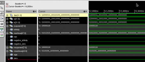
The simulation for FP addition/ subtraction is shown in Figure 8.
64 point FFT design is used with radix-2^6 SDF algorithm. The input data for the 64 point FFT is transferred to Cache memory and twiddle factor is obtained from the ROM (memory unit).
Figure 8. Floating point 32 bit addition/subtraction simulation results
Figure 9. Simulation result of floating point multiplication
The floating point multiplier is coded with HDL and the simulation is shown in Figure 9.
The following tables give the memory utilization area, power and throughput for 64 point FFT. Table 1 shows the power and area consumption of the “proposed 64 point FFT processor”. The Table 2 provides the performance of the proposed 64 point FFT using floating point 32 bit. From this the proposed FFT processor is better than the available implementation.
Table 1. Area and power consumption of 64-point cached FFT
|
Parameter/Type |
Utilization by the proposed design |
|
Memory size (words) |
128 (32 bit floating point 64 for real and 64 imaginary data |
|
Area gate count (mm2) |
79.81 |
|
Power consumption (mw) |
3.24 |
|
Frequency (MHz) |
120 |
Table 2. Performance comparisons of different pipeline FFT processors
|
Author |
Technology (nm) |
FFT Size |
Frequency MHz |
Area (mm2) |
Power (mw) |
|
Sahoo [26] |
90 |
16-128 |
- |
- |
3.82 |
|
Shih [27] |
90 |
4-2048 |
111.11 |
14.59 |
24.2 |
|
Tsai [28] |
90 |
64 |
394 |
0.102 |
36 |
|
Proposed |
90 |
64 |
120 |
79.81 |
3.24 |
The proposed system is synthesized by using CADENCE RTL COMPLIER and is implemented in ENCOUNTER RTL TO GDSII SYSTEM” using 90nm CMOS technology. Figure 10 shows chip layout for the floating point FFT using 64 point.
Figure 10. Chip layout of 64-point FFT processor
In this paper, area efficient low power FFT processor using floating point 32 bit complex input for OFDM systems is proposed. Here we adopted cached memory FFT architecture to reduce the overall memory power consumption. Using floating point multiplier and adder algorithm to design FFT processor core “which integrates 65,385 transistors in area 79.81mm2 with 90nm technology”. The processor can able to execute a 64 point floating point 32 bit complex data with operating frequency of 120 MHz finally; the proposed design of FFT with cache memory can meet IEEE 802.11a standards. Our future work is mainly focused on Reconfigurable FFT/IFFT processor for 5th generation systems.
[1] Baas, B.M. (1999). An approach to low-power, high-performance fast fourier transform processor design. Ph.D. Thesis, Stanford University, Stanford, CA, USA.
[2] Miyamoto, N., Karnan, L., Maruo, K., Kotani, K., Ohmi, T. (2003). A small-area high-performance 512-point 2-dimensional FFT single-chip processor. in European Solid-State Circuits Conference, Estoril, Portugal, pp. 603-606. https://doi.org/10.1109/ESSCIRC.2003.1257207
[3] Kuo, J.C., Wen, C.H., Wu, A.Y. (2003). Implementation of a programmable 64–2048-point FFT/IFFT processor for OFDM-based communication systems. 2003 IEEE International Symposium on Circuits and Systems (ISCAS), Bangkok, Thailand. https://doi.org/10.1109/ISCAS.2003.1205908
[4] He, S., Torkelson, M. (1998). Designing pipeline FFT processor for OFDM (de)modulation. 1998 URSI International Symposium on Signals, Systems, and Electronics. Conference Proceedings (Cat. No.98EX167), Pisa, Italy. https://doi.org/10.1109/ISSSE.1998.738077
[5] Lin, Y.W., Liu, H.Y., Lee, C.Y. (2005). A 1-GS/s FFT/IFFT processor for UWB applications. IEEE J. Solid-State Circuits, 40(8): 1726-1735. https://doi.org/10.1109/JSSC.2005.852007
[6] Wey, C.L., Tang, W.C., Lin, S.Y. (2007). Efficient memory-based FFT architectures for digital video broadcasting (DVB-T/H). 2007 International Symposium on VLSI Design, Automation and Test (VLSI-DAT), Hsinchu, Taiwan. https://doi.org/10.1109/VDAT.2007.373250
[7] Panda, P.R., Nakamura, H., Dutt, N.D., Nicolau, A. (1997). A data alignment technique for improving cache performance. Proceedings International Conference on Computer Design VLSI in Computers and Processors, Austin, TX, USA. https://doi.org/10.1109/ICCD.1997.628925
[8] Lin, Y.T., Tsai, P.Y., Chiueh, T.D. (2005). Low-power variable-length fast Fourier transform processor. I IEE Proceedings - Computers and Digital Techniques, 152(4): 499-506. https://doi.org/10.1049/ip-cdt:20041224
[9] Fu, B., Ampadu, P. (2009). An area efficient FFT/IFFT processor for MIMO-OFDM WLAN 802.11n. Journal of Signal Processing Systems, 56(1): 59-68. https://doi.org/10.1007/s11265-008-0264-9
[10] Chang, Y., Park, S.C. (2004). An enhanced memory assignment scheme for memory-based FFT processor. IEICE Transactions on Fundamentals of Electronics Communications and Computer Sciences, E87A(11): 3020-3024.
[11] Reisis, D., Vlassopoulos, N. (2008). Address generation techniques for conflict free parallel memory addressing in FFT architectures. IEEE Trans. Circuits Syst. I, Reg. Papers, 55(11): 3438-3447. https://doi.org/10.1109/ICECS.2006.379653
[12] Radhouane, R., Liu, P., Modlin, C. (2000). Minimizing the memory requirement for continuous flow FFT implementation Continuous flow mixed mode FFT (CFMM-FFT). 2000 IEEE International Symposium on Circuits and Systems (ISCAS), Geneva, Switzerland. https://doi.org/10.1109/ISCAS.2000.857040
[13] Lin, Y.W., Liu, H.Y., Lee, C.Y. (2005). A 1-GS/s FFT/IFFT processor for UWB applications. IEEE J. Solid-State Circuits, 40(8): 1726-1735. https://doi.org/10.1109/JSSC.2005.852007
[14] Lin, Y.W., Lee, C.Y. (2007). Design of an FFT/IFFT processor for MIMO OFDM systems. IEEE Trans. Circuits Syst. I, Reg. Papers, 54(4): 807-815. https://doi.org/10.1109/TCSI.2006.888664
[15] Lin, Y.W., Liu, H.Y., Lee, C.Y. (2004). A dynamic scaling FFT processor for DVB-T applications. IEEE J. Solid-State Circuits, 39(11): 2005-2013. https://doi.org/10.1109/JSSC.2004.835815
[16] Bass, B.M. (1999). A low-power high-performance, 64-point FFT processor. IEEE J of Solid-state Circuit., 34(3): 380-387. https://doi.org/10.1109/4.748190
[17] Li, W., Wanhammar, L. (1999). A pipeline FFT processor. 1999 IEEE Workshop on Signal Processing Systems. SiPS 99. Design and Implementation (Cat. No.99TH8461), Taipei, Taiwan, pp. 654-662. https://doi.org/10.1109/SIPS.1999.822372
[18] Bidet, E., Castelain, D. (1995). A fast single-chip implementation of 8192 complex point FFT. IEEE Journal of Solid-State Circuits, 30(3): 300- 305. https://doi.org/10.1109/4.364445
[19] Hui, C.C.W., Ding, T. (1996). A new FFT architecture and chip design for motion compensation based on phase correlation. Preceding of International Conference, Application Specific Systems Architectures and Processors, Chicago, IL, USA, pp. 83-02. https://doi.org/10.1109/ASAP.1996.542804
[20] Jia, L.H., Gao, Y., Isoaho, J., Tenhunen, H. (1999). A new VLSI-oriented fft algorithm and implementation. Proceedings Eleventh Annual IEEE International ASIC Conference (Cat. No.98TH8372), Rochester, NY, USA, pp. 337-341. https://doi.org/10.1109/ASIC.1998.723029
[21] Nicola, M., Masera, G., Zamboni, M., Ishebabi, H., Kammler, D., Ascheid, G., Meyr, H. (2005). FFT processor: A case study in ASIP development. IST MobilecSummit, Dresden, Germany.
[22] Heo, K.L., Cho, S.M., Lee, J.H., Sunwoo, M.H. (2003). Application specific DSP architecture for fast fourier transform. Proceedings IEEE International Conference on Application-Specific Systems, Architectures, and Processors, The Hague, Netherlands, pp. 369-377. https://doi.org/10.1109/ASAP.2003.1212860
[23] Hoffmann, A., Schliebusch, O., Nohl, A., Braun, G., Meyr, H. (2001). A methodology for the design of application specific instruction set processors (ASIP) using the machine description language LISA. IEEE/ACM International Conference on Computer Aided Design. ICCAD 2001. IEEE/ACM Digest of Technical Papers (Cat. No.01CH37281), San Jose, CA, USA. https://doi.org/10.1109/ICCAD.2001.968726
[24] Schliebusch, O., Chattopadhyay, A., Kammler, D., Ascheid, G., Leupers, R., Meyr, H., Kogel, T. (n.d.). (2005). A framework for automated and optimized ASIP implementation supporting multiple hardware description languages. Proceedings of the ASP-DAC 2005. Asia and South Pacific Design Automation Conference, Shanghai, China. https://doi.org/10.1109/aspdac.2005.1466174
[25] Ganjikunta, G.K., Sahoo, S.K. (2017). An area-efficient and low-power 64-point pipeline Fast Fourier Transform for OFDM applications. Integration, 57: 125-131. https://doi.org/10.1016/j.vlsi.2016.12.002
[26] Kumar, G.G., Sahoo, S.K. (2020). Area and power-efficient variable-length fast Fourier transform for MR-OFDM physical layer of IEEE 802.15.4-g. IET Computers & Digital Techniques, 14(5): 193–200. https://doi.org/10.1049/iet-cdt.2018.5260
[27] Shih, X.Y., Chou, H.R. (2017). Reconfigurable VLSI design of changeable hybrid-radix FFT hardware architecture with 2D-FIFO storing structure for 3GPP LTE systems. ICT Express, 4(3): 144-148. https://doi.org/10.1016/j.icte.2017.11.007
[28] Tsai, P.Y., Chen, C.W., Huang, M.Y. (2011). Automatic IP generation of FFT/IFFT processors with word-length optimization for MIMO-OFDM systems. EURASIP Journal on Advances in Signal Processing, 2011: 136319. https://doi.org/10.1155/2011/136319