Mourad Bella* | Mehdi Ghoumazi
© 2022 IIETA. This article is published by IIETA and is licensed under the CC BY 4.0 license (http://creativecommons.org/licenses/by/4.0/).
OPEN ACCESS
Today's electronics scenario finds itself with the advancement in the field of foremost important component MOSFET. Though one-step ahead of MOSFET, power MOS transistor such as VDMOS has recently begun to rival bipolar devices in power handling capability. In this paper, the results of simulation of VDMOS transistor have been presented. Additionally, the transfer characteristics of the VDMOS transistor are simulated. The drain current (Ids) as a function of the gate voltage and of the drain voltage was simulated for different work function values as well as for several oxide thickness and gate lengths, respectively. The results obtained show that when the work function and the oxide thickness as well as the gate length increase, the threshold voltage also increases. The VDMOS transistor is virtually fabricated using ATHENA software and simulation is done with help of ATLAS software and all graphs are plotted using Tonyplot in Silvaco.
VDMOS transistor, threshold voltage, work function, software Silvaco-TCAD
The microelectronics of today, like that of tomorrow, will be one of the crucial engines in the construction of the new information and communication society of the 21st century. Because it consists in the miniaturized realization of increasingly complex electronic functions on a single support (silicon in general). At first, the objective of microelectronics was to reduce the weight and volume of devices, but these two criteria have become secondary in the face of improving reliability and the integration density and speed of circuits. It has been largely dominated for years by CMOS integrated circuit technology [1-4]. CMOS technology is a planar technology intended for the development of very high-scale integration systems. VLSI (Very large scale integration). Thanks to the properties of complementary MOS transistors (rated CMOS for Complementary Metal Oxide Silicon), this technology is based on n-MOSFET and p-MOSFET transistors [5, 6].
The constant progress of technological processes concerning microelectronics currently allows enormous advances to be made in the field of integration. In the same system, control components operating under a few volts (CMOS) and so-called power switches that can switch tens of volts and conduct currents of several amperes (LDMOS, IGBT or VDMOS). This type of integration is called “Smart Power Integrated circuit”, which can be translated as “intelligent” power integrated circuit [7-10]. In power electronics, bipolar transistors [11] and Thyristors [12] were the first command power devices that can be used in several power applications, but these devices are not suitable for high frequency switching applications. On the other hand, the evolution of technologies in the field of integrated circuits has allowed the development of power MOSFET transistors capable of operating at high frequency, such as VDMOS transistors [13], LDMOS [14].
The VDMOS transistor is a power transistor fabricated using the MOS double diffusion process. The source and the gate are located on the surface of the chip while the drain is located at the back of the chip. This transistor can amplify electric energy and quickly interrupt the flow of electric current at high speeds, while itself consuming less amount of energy. The VDMOS makes it possible to ensure, thanks to its vertical structure, a passage of strong currents by the parallel connection of a very large number of elementary cells (source-gate). This slide also has the advantage of a high switching speed linked to the absence of storage of minority carriers. And it has a high input impedance and therefore ease of control by the isolated gate. On the other hand, the voltage drop is relatively high in the on state. This is due to the absence of a strong injection plasma zone in the N zone [15-17]. So the VDMOS transistor became Stronger in different applications, such as in high frequency devices, drive power, multiplex bus system and motor drive [18, 19].
Figure 1. VDMOS transistor
In this paper is a presented characteristic of VDMOS transistor of electrical parameters like drain current, gate voltage employing the ATHENA fabrication simulator to fabricate while ATLAS simulator to characterize the device electrically [20]. In ATLAS, the transfer characteristic was generated by fixing the drain voltage (Vds) at a fixed value, e.g., 5V and 15V, and then ramping the gate voltage from 0V to 10V with the step of 0.2V using a sequence of SOLVE statement of the program. In addition, the impact of work function, oxide thickness and gate length on drain current are presented.
The VDMOS transistor used in this study were fabricated on P-type (100) wafer, which ensures a better quality of gate oxide. We will describe the process of this manufacture by the following steps: The first step consists in the oxidation of the substrate to have a layer of silicon oxide SiO2 (range between 0.5 and 2 nm), from which a temperature is applied in an interval, which goes from 800 to 1000℃ for 35min in order to define the oxide of gate.-The second step consists in depositing a layer of polysilicon with a thickness of 500nm by adding by diffusion a layer of passivation with a thickness of 50nm of silicon oxide (SiO2). -Then, the third step is based on the deposition of nitrided silicon by the PECVD method with a layer thickness of 500nm, followed by dry etching of silicon nitride.-The next step is to dope uniformly by the ion implantation method, the etch part using boron with a dose of 5*1013 /cm3 and an energy of 100 Kev to have the body P, after in fact a thermal annealing, then we move on to the diffusion of boron impurities to have a doping depth of 2 μm leaving our pattern under a temperature of 1100℃ for 60 min.
After that, we do a dry oxidation to have a layer of silicon oxide, under a temperature of 800℃ up to 1050℃ with the use of 6.2*107 of O2 for 5 to 20 minutes. Moreover, at the end, we make a diffusion using phosphorus impurities under a temperature of 800 to 900 ℃ for 10 to 20 minutes.
Photo lithogravure-1: This operation consists of depositing a photosensitive resin in a thin and uniform film with a thickness of 0.2 μm followed by a step of etching the resin of the unprotected region. The last technological step consists in depositing a thickness of 0.75μm of aluminum.
Photo lithogravure-2: This step consists of depositing a resin on aluminum followed by an etching of the unwanted regions to have contact with the source.
The final result of the fabrication process is shown in Figure 2.
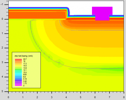
Figure 2. Simulated net doping of power VDMOS using Silvaco tool
The net doping profile of the VDMOS structure is shown on Figure 3.
Figure 3. Simulated net doping profile
3.1 I_V characteristics
The software Silvaco-Atlas was used to construct and simulate the structure and characteristics electrical of the VDMOS structure (Figure 1).
In Figure 4, Ids-Vgs transfer characteristic is shown on a linear scale for VDMOS transistor. On Figure 4 in linear region extracting threshold voltage the value is 3.34 V at Vds=10V. Threshold voltage of the device is an important parameter, which decides the device performance. The threshold voltage expression in case of VDMOS transistor can be expressed by Marcault et al. [21-23]:
$V_t=\frac{t_{o x} \sqrt{4 \varepsilon_{s i} k T \ln \left(n_{A P} / n_i\right)}}{\varepsilon_{o x}}+2 \emptyset_m$ (1)
where, $\emptyset_m=\frac{k T}{q} \ln \left(\frac{n_{A P}}{n_i}\right)$, semiconductor work function, tox is the gate oxide thickness, εsi and εox are, respectively, silicon and oxide permitivities, nAP is the doping concentration and ni is the intrinsic concentration.
The drain current can be calculated in saturation region by Surbhi Sharma Vani and Shivani [24]:
$I_{d s}=\mu_n \frac{w}{L}\left(V_{g s}-V_t\right) C_{o x} V_{c h}-\frac{1}{2} V_{c h}^2$ (2)
And for the high drain voltage, can be expressed by [10]:
$I_{d s}=\frac{1}{2} \mu_n \frac{w}{L} C_{o x}\left(V_{g s}-V_t\right)^2$ (3)
where, μn is the electron channel mobility (cm2/(V.s)); L is the channel length (µm); w is the channel width (µm); Cox is the capacitance of gate oxide (µF); Vch is the voltage drop along the channel inversion (V).
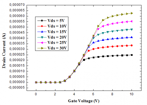
Figure 5 shows the transfer characteristic of the VDMOS transistor, for different drain voltages such as Vds=5V up to Vds=30V.
In Figure 5, it is observed that as the gate voltage increases above the threshold voltage, the conductance increases. As a result, a larger current will flow when the gate voltage is higher than the threshold voltage and the drain voltage is increased.
Figure 4. Transfer characteristic at Vds=10V
Figure 5. Transfer characteristic for different drain voltage
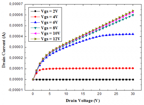
The drain current as a function of the drain voltage for different gate voltages is shown in Figure 6. The effect of the gate voltage on the output characteristics (Ids-Vds) was also observed.
Figure 6. Output characteristic for different gate voltages
The results obtained clearly show a good saturation region of the device at higher gate bias, and the drain current is larger for gate voltages increase.
3.2 Work function effect
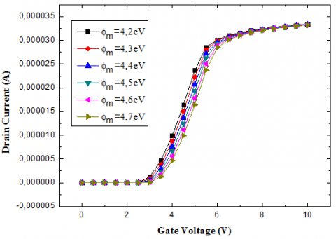
It is very useful to consider the impact of output work on device current and performance.
In Figure 7, we present the effect of output work for different gate voltages. We notice that the lower the output work, the greater the drain current.
Since the work function of the metal is low, this causes the number of carriers, which cross the metal-semiconductor barrier to become greater. And we notice the more the low output work the threshold voltage decreases (Figure 8).
Figure 7. Influence of the gate work function on the drain current for different gate voltage
Figure 8. Threshold voltage versus gate work function
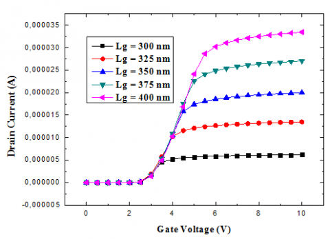
3.3 Gate length effect
The drain current in dependence on the bias voltages, canal length has been carefully investigated. Figure 9 represent Ids (Vgs) characteristics for different channel lengths. It can observe that when channel length decrease, drain current increase.
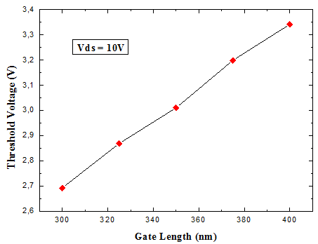
In addition, we can observe too, influence the channel length on threshold voltage represented on Figure 10.
Figure 9. Influence of the channel length on the drain current
Figure 10. Threshold voltage versus gate length
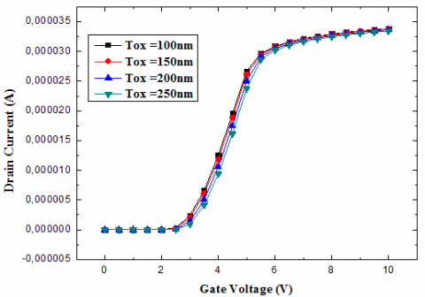
3.4 Oxide thickness effect
Figure 11 presents the drain current versus the gate voltage for different oxide thickness for the VDMOS transistor. It can be seen that when the oxide thickness increases the drain current decease. This is because electric field responsible for drain current increase with increases in gate voltage and decrease with oxide thickness. Also, Figure 12 presents the threshold voltage versus oxide thickness. We can observe the increase of threshold voltage when the oxide thickness increases thus means that there is a linear relationship between the two parameters studied.
(a)
(b)
Figure 11. Influence of the oxide thickness on the drain current lineair (a) and log scale (b)
Figure 12. Threshold voltage versus oxide thickness
In this paper, results of the simulate I_V characteristics of VDMOS transistor using Silvaco-TCAD are presented. According to these simulation results, it is found that when channel length decrease, drain current increase; as well as lead to a decrease of the threshold voltage dramatically. In order to have an acceptable threshold voltage we study the influence of the gate function and conclude for optimize the threshold voltage, the solution is to choose a gate metal with a high value of work function.
[1] Fouad, H. (2020). Performance optimization of energy harvesting solutions for 0.18 um CMOS circuits in embedded electronics design. Cogent Engineering, 7(1): 1772947. https://doi.org/10.1080/23311916.2020.1772947
[2] Bespalov, V.A., Dyuzhev, N.A., Kireev, V.Y. (2022). possibilities and limitations of CMOS technology for the production of various microelectronic systems and devices. Nanobiotechnology Reports, 17(1): 24-38. https://doi.org/10.1134/S2635167622010037
[3] Dhar, S., Pattanaik, M., Rajaram, P. (2011). Advancement in nanoscale CMOS device design en route to ultra-low-power applications. VLSI Design, 1–19. https://doi.org/10.1155/2011/178516
[4] Yu, F., Gao, L., Li, L., Cai, S., Wang, W., Wang, C. (2018). Survey of key technologies on millimeter-wave CMOS integrated circuits. In IOP Conference Series: Materials Science and Engineering, p. 012011. https://doi.org/10.1088/1757-899X/351/1/012011
[5] Leyris, C., Martinez, F., Hoffmann, A., Valenza, M., Vildeuil, J.C. (2007). N-MOSFET oxide trap characterization induced by nitridation process using RTS noise analysis. Microelectronics Reliability, 47(1): 41-45. https://doi.org/10.1016/j.microrel.2006.02.010
[6] Chaturvedi, M., Dimitrijev, S., Haasmann, D., Moghadam, H.A., Pande, P., Jadli, U. (2022). Quantified density of performance-degrading near-interface traps in SiC MOSFETs. Scientific Reports, 12(1): 1-9. https://doi.org/10.1038/s41598-022-08014-5
[7] Srivastav, A.K. (2016). Mechanism of power dissipation capability of power MOSFET devices: Comparative study between LDMOS and VDMOS transistors. International Journal of Science and Research, 5(6): 653-656. https://doi.org/10.21275/v5i6.NOV164166
[8] Ramarao, B.V., Mishra, J.K., Pande, M., Singh, P., Kumar, G., Mukherjee, J. (2013). Comparison study of LDMOS and VDMOS technologies for RF power amplifiers. AIP Conference Proceedings, 1512(1): 492-493. https://doi.org/10.1063/1.4791126
[9] Yusof, H.H.M., Murti, W.B., Soin, N. (2011). Design consideration of N-drift region doping concentration in high voltage VDMOS transistor. International Journal of Scientific Research Engineering and Technology, 3(4): 816-819.
[10] Yang, Y., Tang, Z., Zhang, Z., Liu, Y., Wang, Z., Tan, K., Feng, Z. (2011). A novel structure in reducing the on-resistance of a VDMOS. Journal of Semiconductors, 32(2): 024005. https://doi.org/10.1088/1674-4926/32/2/024005
[11] Li, J., Chen, X., Xiao, Y., et al. (2019). A tunable floating-base bipolar transistor based on a 2D material homojunction realized using a solid ionic dielectric material. Nanoscale, 11(46): 22531-22538. https://doi.org/10.1039/C9NR07597F
[12] Arshad, M., Jamil, E., Shuja, A., Qayyum, F., Hassan, G. (2022). Modelling and simulation of design variants for the development of 4H-SiC thyristors. Silicon, 1-13. https://doi.org/10.1007/s12633-022-01766-9
[13] Li, Q., Bao, T., Li, H., Sun, T., Zuo, Y. (2020). Uniform shallow trenches termination design for high-voltage VDMOS transistor. Electronics Letters, 56(2): 104-105. https://doi.org/10.1049/el.2019.2982
[14] Theeuwen, S.J.C.H., Qureshi, J.H. (2012). LDMOS technology for RF power amplifiers. IEEE Transactions on Microwave Theory and Techniques, 60(6): 1755-1763. https://doi.org/10.1109/TMTT.2012.2193141
[15] Xu, H.E., Trescases, O.P., Sun, I.S., et al. (2007). Design of a rugged 60 V VDMOS transistor. IET Circuits, Devices & Systems, 1(5): 327-331. https://doi.org/10.1049/iet-cds:20070008
[16] Williams, R.K., Darwish, M.N., Blanchard, R.A., Siemieniec, R., Rutter, P., Kawaguchi, Y. (2017). The trench power MOSFET: Part I—History, technology, and prospects. IEEE Transactions on Electron Devices, 64(3): 674-691. https://doi.org/10.1109/TED.2017.2653239
[17] Chauhan, Y.S., Anghel, C., Krummenacher, F., et al. (2006). A compact DC and AC model for circuit simulation of high voltage VDMOS transistor. In 7th International Symposium on Quality Electronic Design (ISQED'06), p. 6.
[18] Farhadi, R., Farhadi, B. (2014). Optimization of vertical double-diffused metal-oxide semiconductor (VDMOS) power transistor structure for use in high frequencies and medical devices. Electronic physician, 6(2): 816. https://doi.org/10.14661/2014.816-819
[19] Abdullah, H., Jurait, J., Lennie, A., Nopiah, Z.M., Ahmad, I. (2009). Simulation of fabrication process VDMOSFET transistor using Silvaco software. European Journal of Scientific Research, 29(4): 461-470.
[20] Bhuyan, M.H., Islam, M.T. (2022). Study of an n-MOSFET by designing at 100 nm and simulating using SILVACO ATLAS simulator. Journal of VLSI and Signal Processing, 12(1): 07-15.
[21] Marcault, E., Bourennane, A., Tounsi, P., Breil, M., Dorkel, J.M. (2014). VDMOS electrical parameters potentially usable as mechanical state indicators for power VDMOS assemblies. IET Circuits, Devices & Systems, 8(3): 188-196. https://doi.org/10.1049/iet-cds.2013.0231
[22] Marcault, E., Bourennane, A., Tounsi, P., Breil, M., Dorkel, J.M. (2014). VDMOS electrical parameters potentially usable as mechanical state indicators for power VDMOS assemblies. IET Circuits, Devices & Systems, 8(3): 188-196. https://doi.org/10.1049/iet-cds.2013.0231
[23] Baliga, B.J. (1998). Chapter power devices of modern semiconductor device physics. pp. 209-211.
[24] Surbhi Sharma Vani, G., Shivani, S. (2016). A review on VDMOS as a power MOSFET. Journal of Electronics and Communication Engineering, 119-124. https://doi.org/10.9790/2834-15010119124