Mahamdasraf A. Mulla* | Vishal J. Dobariya | Rajan V. Vamja | Arindam Sircar
© 2021 IIETA. This article is published by IIETA and is licensed under the CC BY 4.0 license (http://creativecommons.org/licenses/by/4.0/).
OPEN ACCESS
The bidirectional dc-dc converter with high voltage gain and high efficiency plays an important role in the designing of battery charging systems. In this paper, design and development of a battery charging system utilizing coupled inductor based high gain dc-dc converter is presented. The converter uses a clamp capacitor network to recover the leakage energy of a coupled inductor. The converter has inherent soft-switching capability during turn ON, which ensures high efficiency at high switching frequency. Design equations to derive value of different passive components are given and a step-wise exclusive design to construct coupled inductor is presented. A 50 kHz, 500 W laboratory prototype has been designed, which can increase the voltage with 10 gain (boost operation) in one direction and can reduce the voltage at (1/10) gain (buck operation) in other direction. The CCCV battery charging algorithm is implemented using generic ARM Cortex-M4 microcontroller. Extensive experiments have been performed and the experimental results are presented in buck, boost, and battery charging operations.
battery charging, bidirectional DC-DC converter, high voltage gain, coupled inductor
Due to the intermittent nature of renewable sources, secondary storage device like batteries have become indispensable in many applications. Batteries are an essential part of many power electronic applications like AC-DC microgrids, elevators, electric vehicles, etc. [1, 2]. A major technical challenge arises in interfacing batteries with system voltages due to the difference in the level of voltage ratings between them. Design of power electronic converters with required high step-up or step-down gain becomes an important aspect [3, 4]. Therefore, the interfacing circuits in such applications require a DC-DC converter with bidirectional power flow and high voltage conversion ratio. Batteries have limited charge-discharge life period [5, 6]. It is therefore required to charge them with constant-current (CC) or constant-voltage (CV) by knowing the state of charge of the batteries. The control of power electronic converters for photovoltaic applications is another task. Some control strategies using Artificial Neural Networks and Fuzzy logic control have been studied by Fapi et al. [7], Jayaraju and Rao [8]. The performance analysis of different controllers for hybrid energy systems has been shown by Katuril and Gorantla [9, 10].
The efficiency of conventional BDC reduces drastically when operated with high duty cycle to achieved HV conversion ratios [11]. This is because of practical circuit drops like device drops, drop due to equivalent series resistance (ESR) of inductor, capacitor etc. The efficiency of such BDC declines with low or higher duty cycle, thereby limiting its conversion ratio [12]. The application of such BDC is limited in battery charging as it cannot achieve HV conversion ratios efficiently. Several BDCs are proposed to achieve energy efficient HV conversion. They are based on high frequency transformer, coupled inductor, switching capacitor, switching inductor, voltage lift technique, voltage multiplier technique etc. [13-16].
In high-frequency transformer based BDC topologies, the turns ratio of the transformer provides the HV conversion [17]. The topologies based on dual active bridge are evolved as higher voltage gain bidirectional DC-DC converter configurations. These topologies involve a large number of switches resulting in high switching loss, which can be reduced by using soft-switching schemes presented by Yang and Do [18]. However, this leads to complex configurations and control. It is also required to protect the switches against HV spikes resulting from the leakage inductance of the isolation transformer. Snubber circuits are utilized to limit these voltage spikes. A snubber capacitor stores the leakage energy during the turn OFF time of switch. This energy is dissipated in the snubber resistor or retrieved by recycling it. Recycling energy requires an active clamping circuit having additional switches and an extra transformer, which makes the BDC bulky and complex [19]. Non-isolated BDC topologies derived from flyback and forward converters have been researched but their implementation is limited to low-power applications [20, 21]. BDCs based on a switched capacitor have also been researched by Amjadi and Williamson [22]. These arrangements required large number of switches and capacitors for HV conversion, which makes the circuit complicated. The voltage multiplier-based topology needs several cells with high rating, which results in high voltage stresses on the components. Switched inductor and voltage lift technique is not suitable for high power application as it requires a large number of passive components.
In another approach, for HV conversion using BDC, coupled inductor-based topologies are proposed by Hsieh et al. [23]. These converters have less circuit components as compared to the prior transformer and switched capacitor-based topologies. Bipolar core excitation is also possible in these converters, which make them suitable for high-power and high efficiency applications. However, in these arrangements as well, the presence of leakage energy necessitates the use of a clamp capacitor network for the safe operation of switches. High voltage gain of such configurations can be increased with an intermediate capacitor at the secondary of the coupled inductor. Many topologies of coupled inductor based BDC with clamped capacitor have been studied to minimize the numbers of circuit components. Out of them, the BDC proposed by Shreelakshmi et al. [24] has fewest components, i.e., a coupled inductor, a clamp and an intermediate capacitor, and four power electronics switches. In this topology, the efficiency is improved by recovering the leakage energy in the clamp capacitor. All switches achieve an inherent soft-switching during turn ON, which reduces switching losses and increases efficiency.
In summary, high gain dc-dc converters are essential for interfacing low voltage source with high voltage dc link in the distributed generation environment [25]. The key objective of the presented study are as follows:
1) To develop a charging circuit to charge the lead acid and/or lithium-ion batteries. Accordingly, the constant current (CC) and constant voltage (CV) charging methods are implemented.
2) The real time implementation of the coupled inductor based, soft switched, high gain BDC for battery charging application is presented. The complete design steps of the selected converter are demonstrated.
3) The high voltage gain is achieved through the use of a coupled inductor and an intermediate capacitor. The topology ensures ZVS during turn-on for all active switches over the entire battery charging range, which enhances the efficiency.
4) The control circuit of the converter is realized using generic low-cost ARM Cortex-M4 microcontroller STM32F407VG from ST Microelectronics.
5) The converter is designed at 50 kHz high switching frequency, which makes the size of the converter compact. Also, the use of general-purpose microcontroller makes the converter cost effective.
The implemented high gain BDC consists of a coupled inductor, four switches, a clamp and an intermediate capacitor. The leakage energy is recovered using the clamp capacitor, which improves efficiency. The coupled inductor and intermediate capacitor are utilized to achieve the high voltage gain. At the secondary of the coupled inductor, the intermediate capacitor is charged in series and discharged in parallel during buck operation. The operation is vice versa during the boost mode. The converter has soft switching capability for all switches.
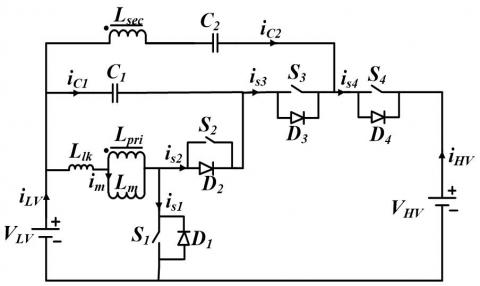
The circuit schematic of the implemented BDC for the battery charging application is shown in Figure 1. The circuit consists of two capacitors and one coupled inductor. C1, C2 are a clamp capacitor and an intermediate capacitor, respectively. There are four switches (S1-S4) along with anti-parallel body diodes (D1-D4). L1 and L2 are the inductances of the low voltage (LV) and high voltage (HV) windings of the coupled inductor, respectively.
In the presented DC-DC converter, the leakage energy in the coupled inductor is recovered using the clamp capacitor C1. Due to the recycling of this leakage energy, the losses are less and efficiency is higher in the BDC. The voltage spikes across the switches are also reduced and the converter becomes more reliable. C2 is used for an intermediate energy storage which helps to increase the voltage conversion ratio. Due to the higher voltage conversion ratio and the ZVS capability of the switches, the presented BDC is a suitable choice for battery charging application. The operation of the presented BDC is explained for boost and buck modes in subsequent sections.
Figure 1. Circuit configuration of implemented high gain bidirectional DC-DC converter
2.1 Boost mode of operation
(a)
(b)
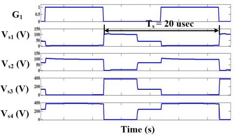
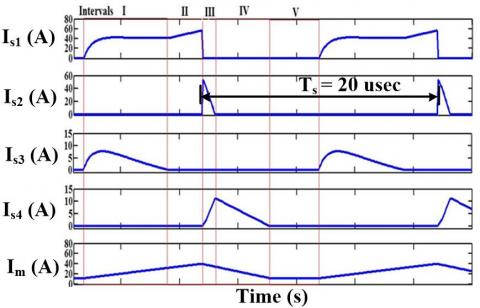
Figure 2. Steady-state waveforms in boost mode: (a) gate pulses and voltage across switches; and (b) current through different switches
Figure 3. Steady-state waveform of input-output parameters of presented BDC during boost mode: VLV, VHV, ILV, and IHV
The boost mode of operation is divided into five intervals as shown in Figure 2 and Figure 3. Figure 2 shows the steady-state waveforms of the current through and the voltage across all switches. Figure 3 shows the steady-state waveforms of the current through and the voltage across the inductor. During interval I, switch S1 is turned ON. The current flows from the battery to the coupled inductor. Energy is stored in the magnetizing inductance of the coupled inductor and the capacitor C2 through the secondary winding of the coupled inductor and the capacitor C1. The body diode D3 is forward biased due to the induced voltage in the coupled inductor. In Interval II, current through D3 becomes zero. The current through S1 increases linearly. This interval ends when S1 is turned OFF.
During interval III, D2 is forward biased due to the energy stored in the leakage inductance and the charge of the clamp capacitor C1. Additionally, during this interval the stored coupled inductor energy is transferred to the load through the inductor L2, the capacitor C2, and the diode D4. The interval ends when the current flowing in D2 becomes zero. During interval IV, D2 turns OFF and D4 continues to conduct. This interval ends when the current through D4 becomes zero. In interval V, none of the switches are in conduction.
Interval V ends when S1 is turned ON. From the steady-state analysis, the voltage gain equation for boost mode can be written as:
$\frac{V_{H V}}{V_{L V}}=\frac{n+1}{1-D}$ (1)
where, VHV, VLV are the high voltage and low voltage side voltages, respectively. n is turns ratio of the coupled inductor. D is the duty cycle of switch S1.
2.2 Buck mode of operation
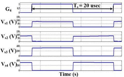
The buck mode of operation is divided into six different intervals as shown in Figure 4. The voltage and current waveforms of all the switches are observed in Figure 4 whereas the voltage and the current waveforms of the coupled inductor are shown in Figure 5. In interval I, S2 is turned ON, and current flows from C1 to the primary winding of the coupled inductor. In this interval, the body diode of S4 starts to conduct when S4 is triggered. ZVS is observed during turn ON of S4 as shown in Figure 4(b). In interval II, only switch S4 conducts and energy is stored in the coupled inductor through the secondary winding. This interval is similar to the turn ON mode of the conventional buck converter. This interval ends when S4 is turned OFF.
(a)
(b)
Figure 4. Steady-state waveforms in buck mode: (a) gate pulses and voltage across switches; and (b) current through different switches
Figure 5. Steady-state waveform of input-output parameters of presented BDC during buck mode: VLV, VHV, ILV, and IHV
During interval III, all switches remain OFF, and the body diodes of S3 and S1 conduct. This interval ends when S3 is turned ON. Since D3 is already in conduction, ZVS is observed during turn ON of switch S3. Interval IV starts with the turning ON of switch S3. Energy is transferred from C2 to C1 through the secondary winding of coupled inductor.
The interval V begins when the current through D1 becomes zero. Current through S3 continues during interval V. This interval ends when S3 is turned OFF. Due to turning OFF of S3, the current through secondary of the coupled inductor forces the body diode of switch S4 to turn ON. Interval VI starts with the turning ON of diode D4. This interval ends when S4 is triggered. From the steady-state analysis, the voltage gain equation for buck mode can be written as:
$\frac{V_{L V}}{V_{H V}}=\frac{D}{1+n}$ (2)
where, D is the duty cycle of switch S4.
The design of the various circuit components of presented high gain DC-DC converter is explained in the next section.
In this section, the design of various circuit components is described. The presented BDC is designed for the ratings given in Table 1. The coupled inductor is designed such that it allows for 10 % current ripple in currents. Additionally, all the capacitors have been designed to limit voltage ripple to 0.1 % of rated voltage.
Table 1. Ratings considered for design of different components of BDC
|
Parameters |
Values |
|
Power |
500 W |
|
VHV |
400 V |
|
VLV |
40 V |
|
fsw |
50 kHz |
|
Voltage Ripple |
0.1 % |
|
Current Ripple |
10 |
3.1 Design of coupled inductor
The design of coupled inductor is essential for the BDC. For CCM operation, turns ratio n and duty cycle D is obtained using Eq. (1) and Eq. (2) for boost mode and buck mode, respectively.
For DCM operation, voltage gain of the presented BDC in boost mode is expressed as:
$\frac{V_{H V}}{V_{L V}}=\frac{1+n}{2}+\frac{\sqrt{(1+n)^{2}+\frac{2 D^{2} T_{S} R_{L V}}{L_{1}}}}{2}$ (3)
where, RLV is the low voltage side load resistance. Ts is the switching period. L1 is the primary side inductance value of the coupled inductor.
The critical inductance of primary winding of coupled inductor L1crit is obtained by equating Eq. (1) and Eq. (3). This is expressed as:
$\frac{L_{1 c r i t}}{T_{S} R_{H V}}=\frac{(1-D)^{2} D}{2(1+n)^{2}}$ (4)
where, RHV is the HV side load resistance. L1 is the primary side inductance value of the coupled inductor.
The critical inductance of secondary winding L is obtained using the following equation:
$L_{2 c r i t}=n^{2} L_{1 c r i t}$ (5)
where, L1crit is the primary side critical inductance.
The practical values of inductors (L1 and L2) are selected as approximately 3 times the critical values for CCM operation. Accordingly, it is calculated to be 45 µH and 720 µH for L1 and L2, respectively.
3.2 Design of capacitors
Designs of different capacitors are given in following subsections.
3.2.1 Design of the capacitor CHV
During interval I of boost mode, CHV supplies the load current and its value is calculated as:
$C_{H V}=\frac{I_{H V} D}{f_{s w}(0.001) V_{H V}}$ (6)
where, IHV is the high voltage side source current. fsw denotes the switching frequency.
By considering the coupled inductor current ripple, the value of capacitor CHV is selected as:
$C_{H V}=\frac{\left(\frac{n+1}{1-D}-1\right) V_{L V}}{8 L_{m} f_{s w}^{2}(0.001) V_{H V}}$ (7)
where, Lm is the magnetizing inductance of coupled inductor.
To minimize voltage ripple, higher value amongst Eq. (6) and Eq. (7) is selected.
3.2.2 Design of the capacitor CLV
The capacitor CLV is utilized to filter out inductor current ripple. Based on the ripple current magnitude, the minimum value of the capacitance is calculated as:
$C_{L V}=\frac{1-\left(\frac{D}{1+n}\right) V_{L V}}{8 L_{m} f_{s w}^{2}(0.001) V_{L V}}$ (8)
The capacitor CLV also supplies current during the buck operation. Hence, it is evaluated as:
$C_{H V}=\frac{I_{L V} D(0.05)}{f_{s w}(0.001) V_{L V}}$ (9)
where, ILV is the low voltage side source current.
3.2.3 Design of Capacitor C2
This capacitor is charged in parallel with secondary winding during boost operation and is discharged in series with the secondary of the coupled inductor to obtain high conversion ratio. In buck mode, the opposite operation occurs.
$V_{C 2}=\frac{D(1-n)+n}{1-D} V_{L V}$ (10)
From Eq. (10), the average voltage across the capacitor can be obtained. For the ripple voltage of 0.1 %, The value of capacitor C2is calculated as:
$C_{2}=\frac{I_{L V} D}{n f_{s w}(0.001) V_{C 2}}$ (11)
3.2.4 Design of the capacitor C1
From Eq. (12), the average value of voltage across C1 is obtained for buck and boost operation as:
$V_{C 1}=\frac{D V_{H V}}{1+n}$ (12)
In interval II for boost operation, and in interval IV of buck operation, the capacitor C1 is charged and value is calculated as:
$C_{1}=\frac{I_{L V} D(0.05)}{f_{s w}(0.001) V_{C 1}}$ (13)
The calculated values for CHV, CLV, C2 and C1 are 330 µF, 200 µF, 50 µF and 10 µF, respectively.
3.3 Design of switches
The switches are designed to carry RMS current when they are ON and withstand the average drain to source voltage across the switch when they are OFF. The RMS values of switches is observed during simulation study. The basic design equations are mentioned below.
The RMS value of current through the switch S1 is calculated as:
$I_{S 1 r m s}=\frac{n V_{L V} T_{S} D \sqrt{D}}{L_{m} \sqrt{3}}$ (14)
The voltage across the switch S1 is calculated as:
$V_{S 1}=\frac{1}{l-D} V_{L V}$ (15)
The RMS value of current through the switch S2 is calculated as:
$I_{S 2 r m s}=\frac{0.05^{1.5} V_{C 1} T_{S} D \sqrt{D}}{L_{l k} \sqrt{3}}$ (16)
The voltage across the switch S2 is calculated as:
$V_{S 2}=\frac{1}{1-D} V_{L V}$ (17)
The RMS value of current through the switch S3 is calculated as:
$I_{S 3 r m s}=\frac{V_{L V} T_{S} D \sqrt{D}}{L_{m} \sqrt{3}}$ (18)
The voltage across the switch S3 is calculated as:
$V_{S 3}=2 n V_{L V}$ (19)
The RMS value of current through the switch S4 is calculated as:
$I_{S 4 r m s}=\frac{V_{L V} T_{S} D \sqrt{D}(1-D)}{(n+1) L_{1} \sqrt{3}}$ (20)
The voltage across the switch S4 is calculated as:
$V_{S 4}=\frac{n}{1-D} V_{L V}$ (21)
The rating of the switches for the BDC is shown in Table 2.
3.4 Construction of coupled inductor
This section presents the construction of the coupled inductor using the values of L1and L2 as determined in Section 3.1.
3.4.1 Area product
The amount of energy stored in a coupled inductor is calculated as:
$E_{L}=\frac{1}{2} L_{1} I_{m}^{2}$ (22)
where, Im is the maximum magnetizing current through the coupled inductor.
The current in the primary winding during CCM operation increases linearly during the turn ON time and decreases linearly during the turn OFF time. Hence, the average current through the equation is given by:
$I_{m}=I_{\text {L1avg }}+\frac{1}{2} \Delta I_{L 1}$ (23)
where, IL1avg is the average current through inductor and DIL1 is the ripple current through the inductor.
Using Eq. (22), the Area Product of the magnetic core is calculated by the following equation:
$A_{P}=A_{w} A_{C}=\frac{2 E_{L}}{K_{w} K_{c} J B_{m}}$ (24)
where, Aw, Ac, Kw, Kc, Bm and J are the window area of the core, the cross-sectional area of the core, the window space factor, the crest factor, the maximum flux density and the current density in the windings, respectively.
From Eq. (24), the minimum required Area Product for the core is calculated as 11253 mm4.
3.4.2 Selection of core and permeance calculation
The core to be selected should have an area product greater than the one calculated in Eq. (24). The permeance of the core is expressed as:
$\Lambda=\frac{\mu_{0} \mu_{r} A_{C}}{l_{m}+\mu_{r} l_{g}}$ (25)
where, Λ, µr, lm, lg are the permeance, the relative permeability, the magnetic path length and the air gap length, respectively.
Using Eq. (25), the calculated values of permeance of core is 442 nH /turns2.
3.4.3 Calculation of number of turns
The number of turns can be expressed in terms of permeance and inductance as:
$N=\sqrt{\frac{L}{\Lambda}}$ (26)
where, N is the number of turns of the inductor.
The number of turns for primary and secondary windings are calculated as 10 and 40, respectively.
3.4.4 Wire gauge selection
Selection of wire gauge is dependent on the current density of the material and current flowing through to it. The cross- section area of the wire is given as:
$a=\frac{I_{r m s}}{J}$ (27)
where, a is the cross-sectional area of the wire, Irms is the RMS current flowing through the wire and J is the current density.
For the designed BDC, the current density of both primary and secondary windings is equal. The practical value of a is approximated to the nearest value in the SWG table. The calculated value for a1 and a2 are 4.166 mm2 and 0.4166 mm2, respectively. Accordingly, the selected wire gauges are the SWG 13 and SWG 22.
3.4.5 Check for window area available
To accommodate the number of turns calculated using Eq. (26) with the wire gauge selected using Eq. (27), enough space should be available in the window to accommodate the turns. It is confirmed using the following inequality:
$A_{w} K_{w}>a_{1} N_{1}+a_{2} N_{2}$ (28)
All calculated parameters of circuit components are shown in Table 2. By considering the derived value of components for presented BDC, the experimental setup is constructed. The operation of the circuit is verified in boost and buck modes. Moreover, the CCCV battery charging operation is experimented using the designed BDC. The experimental results are discussed in the next section.
Table 2. Calculated value of different components
|
Component |
Values |
|
Coupled Inductor: |
|
|
Duty Ratio (D) |
0.5 |
|
Turns Ratio (n) |
4 |
|
Primary Turns (N1) |
10 |
|
Secondary Turns (N2) |
40 |
|
Primary Inductance (L1) |
45 |
|
Secondary Inductance (L2) |
720 |
|
Window Space Factor (Kw) |
0.3 |
|
Crest Factor (Kc) |
1.05 |
|
Current Density (J) |
3 x 10^6 |
|
Maximum Flux Density (Bm) |
0.8 |
|
Area Product required (Ap) |
11253 |
|
Outer Diameter (Dout) |
52 |
|
Inner Diameter (Din) |
28 |
|
Magnetic Path Length (lm) |
126 |
|
Air Gap Length (lg) |
0 |
|
Cross-Section Area of Core (Ac) |
180 |
|
Window Area of Core (Aw) |
615 |
|
Relative permeability (μr) |
245 |
|
Permeance of core (Λ) |
442 |
|
Cross Section Area of primary winding |
SWG 13 |
|
Cross Section Area of secondary winding |
SWG 22 |
|
Capacitors |
|
|
Input Capacitance (CHV) |
330 μF, 450 V |
|
Output Capacitance (CLV) |
200 μF, 160 V |
|
Clamp Capacitor (C1) |
10 μF, 250 V |
|
Intermediate Capacitor (C2) |
50 μF, 160 V |
|
Switches |
|
|
S1 |
100 V, 15 A |
|
S2 |
100 V, 15 A |
|
S3 |
500 V, 5 A |
|
S4 |
500 V, 5 A |
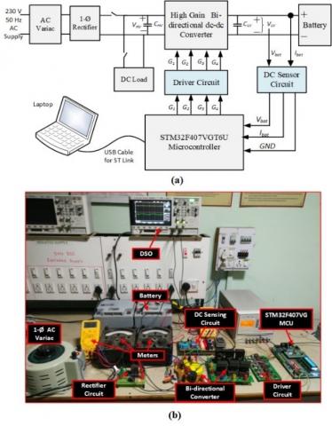
The experimental setup is constructed according to the block diagram shown in Figure 6(a). At the LV side, a lead-acid battery rated 12 V 42 Ah is connected whereas at the HV side, DC load of 320 W and rectified DC voltage source are connected using contactor switches. The BDC consists of SiC MOSFETs (C3M0120090D) as the switches. Hall effect-based DC sensor cards (Nitech make) sense the battery voltage (Vbat) and current (Ibat). These sensed signals are given to the microcontroller, which generates 50 kHz PWM pulses (G1-G4) according to the implemented control system. These pulses are processed though the driver card consisting of a TLP250 optocoupler, which provides optical isolation between the power circuit and control circuit. These isolated pulses drive the SiC switches of the designed BDC. The photograph of the experimental prototype is shown in Figure 6(b).
Figure 6. Experimental setup of high gain bidirectional DC-DC converter: (a) block diagram; and (b) photograph of the prototype
The control is implemented using a general-purpose ARM Cortex-M4 32-bit microcontroller, STM32F407VG. Selected control operates at 168 MHz, and it has required on-chip 12- bit analog to digital converter (ADC) and dedicated high- speed PWM timers. All the voltage and current values are measured utilizing two analog voltmeters and two digital voltmeters. During the experimentation, current and voltage waveforms are captured using a digital storage oscilloscope.
The experiment results are discussed next in three parts. The first and second part presents the performance of the designed BDC in boost mode and buck mode, respectively. These separate experiments are performed to verify the gain and switch voltage stress during the buck and boost mode of the operation. In the third part, the CCCV battery charging scheme is implemented, and results are discussed.
4.1 Experimentation in boost mode of operation
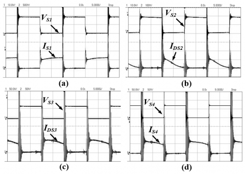
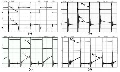
Figure 7. Steady-state waveform of switch voltage and switch current in boost mode: (a) VS1, IS1; (b) VS2, IDS2; (c) VS3, IDS3; and (d) VS4, IS4
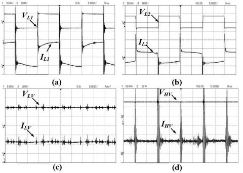
Figure 8. Steady-state waveform of voltage and current in boost mode: (a) primary winding: VL1, IL1; (b) secondary winding: VL2, IL1; (c) low voltage input: VLV, ILV; and (d) high voltage output: VHV, IHV
The experimental results of the boost mode are presented in this section. A 12 V battery is used as a source on the LV side of the BDC. On the HV side, a 320 W rheostat is connected as a load. During boost operation, only switch S1 is operated. Current and voltage waveforms of switch S1 are shown in Figure 7(a). S1 is ON in the interval I and II of boost operation. S1 helps in storing energy from battery to coupled inductor through the primary winding. Figure 7(b) shows the current and voltage waveform of switch S2. Current IDS2 flows through the anti-parallel diode D2 of switch S2. The leakage energy of coupled inductor is transferred to C1 through D2 in interval III of boost operation.
The experimental waveform of the current in diode D3 is shown in Figure 7(c). During intervals I and II, D3 is forward biased, and energy is transferred from C1 to C2. This stored energy is transferred through the diode D4 to the output capacitor and load resistance during intervals III, IV and V as shown in Figure 7(d). The voltage and the current waveforms in the primary winding L1 and secondary winding L2 are shown in Figure 8(a) and Figure 8(b), respectively. The current ratio is found dependent on the external circuit and the amount of energy stored. For the parameters given in Table 3, it is observed that the voltage stress across S1 and S2 is less than 20.0 V while across S3 and S4 is around 80.0 V in boost operation.
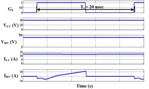
The experimental waveforms of input current and voltage during boost operation are shown in Figure 8(c). During boost mode, input voltage across the battery is 10.8 V and a current of 2.5 A is drawn from the battery. With 50 % duty ratio, the output voltage is observed as 100.2 V and output current is 0.25 A as shown in Figure 8(d). Voltage gain obtained by the BDC is 10 during boost mode of operation.
4.2 Experimentation in buck mode of operation
The experimental results of buck mode are presented in this section. A single-phase AC variac and diode bridge rectifier is used as a source on the HV side of the BDC. On the LV side, a rheostat is connected to perform buck operation in open loop.
Switch S1 is not operated during the buck mode. However, the anti-parallel diode D1 will conduct during intervals III, IV and V. The voltage and the current waveforms of diode D1 is observed in Figure 9(a). Diode D1 transfers energy stored in the leakage inductance and the magnetizing inductance of the coupled inductor. Figure 9(b) shows the voltage and current waveforms of switch S2. When S2 is turned ON, the energy stored in C1 transfers to the primary of the coupled inductor. S2 remains ON during interval I and II.
Figure 9. Steady-state waveform of switch voltage and switch current in buck mode: (a) VS1, IDS1; (b) VS2, IS2; (c) VS3, IS3; and (d) VS4, IS4
Current IS3 through switch S3 and the voltage VS3 across switch S3 are shown in Figure 9(c). S3 is ON during interval IV of the buck operation. Energy transfers from C2 to C1 and L2 through the switch S3. In the buck operation, S4 is the main controlling switch, where the duty cycle of S4 decides the duty cycle of S2 and S3. Switch S4 remains ON during interval I and II of the buck operation. Figure 9(d) shows the experimental waveforms of current through S4 and voltage across S4.
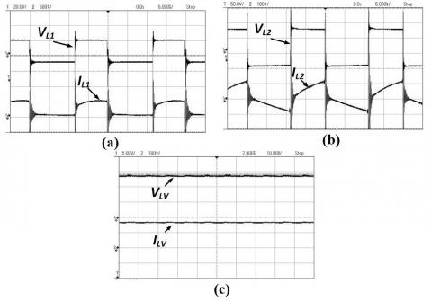
Figure 10. Steady-state waveform of voltage and current in buck mode: (a) primary winding: VL1, IL1; (b) secondary winding: VL2, IL1; (c) low voltage output: VLV, ILV
Figure 10(a) and Figure 10(b) show the voltage and current waveforms of coupled inductor L1 and L2 respectively. The coupled inductor was designed for turns ratio n = 4 which is verified by observing the voltage magnitude across primary and secondary of the coupled inductor. Currents through these windings are not proportioned like voltages because it is dependent on the external circuit and the amount of energy stored. The voltage across load resistance VLV and current through load resistance ILV are shown in Figure 10(c). Load current and voltage both are constant and ripple free.
It is observed that the voltage stress across S1 and S2 is around 30 V while across S3 and S4 is 120 V in buck operation. For the input voltage of 140 V, output of 13.4 V is observed for 50% duty ratio. Hence, an approximate gain of 1/10 is achieved experimentally. The buck mode of operation of the BDC is validated by this experiment.
Table 3. Lead-acid battery charging parameters
|
Parameter |
Value |
|
Input Parameters |
|
|
Supply Voltage |
140 V |
|
Max Input Current |
3 A |
|
Switching Frequency |
50 kHz |
|
Output Parameters |
|
|
Max Battery Voltage |
14.4 V |
|
Max Battery Current |
11.25 A |
4.3 Battery charging application
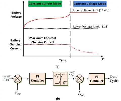
In this section, the BDC is operated to charge a lead-acid battery. The selected pre-set voltage level charging scheme for the six-cell battery is as shown in Figure 11(a). Block diagram of charging voltage regulator is shown in Figure 11(b).
The battery voltage Vbat and the battery current Ibat is sensed using the DC sensor card. Battery voltage is compared with the reference battery voltage. The error is given to a PI controller to generate a reference battery current which is passed through the saturation block to limit it to less than rated charging current. This reference battery current is compared with actual battery current and the error is given to another PI controller.
According to the error, the PI controller adjusts the duty cycle of switching pulse which is generated by the advanced timer (TIM1) of STM32F407VG. The battery charging parameters for lead-acid battery is shown in Table 3.
The programmed values for different phases are given below:
(1) Constant Current Phase: Here, $10 \mathrm{~V} \leq V_{b a t}<14 \mathrm{~V}$ and the constant charging current is 1.5 A.
(2) Constant Voltage Phase: Here, Vbat = 14 V
Figure 11. Lead-acid battery charging: (a) preset voltage level charging scheme for the six-cell battery; (b) block diagram of charging controller
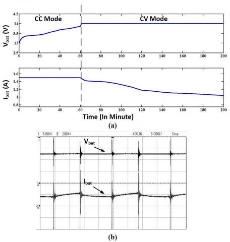
Figure 12. Lead-acid battery charging experiment results:
(a) Graph of experimental results, Vbat vs t and Ibat vs t; and (b) steady-state waveform of Vbat and Ibat.
The experimental results for a 12 V 42 Ah lead-acid battery are shown in Table 4. In this table, input voltage, input current, output voltage, and output current are noted down with respect to time. The output voltage is battery voltage Vbat and the output current is battery charging current Ibat. Initially, due to the battery discharging, battery voltage is less than the pre-set voltage. In this interval, the BDC starts charging through a constant current of 1.5 A. Once the battery voltage reaches the pre-set voltage of 14 V, the BDC starts charging at a constant voltage of 14.4 V and the current starts reducing. The results of Table 4 are plotted and presented in Figure 12(a). The steady-state waveform of charging voltage and current are depicted in Figure 12(b).
The performance of the BDC is observed for boost, buck, and the battery charging operations. Experimentally, the voltage gain is verified as 1/10 in buck mode and 10 in boost mode of operation. During buck mode, the voltage stress on switches S1 and S2 is 30 V and voltage stress on switches S3 and S4 is 120 V. During boost mode, the voltage stress on switches S1 and S2 is 20 V and voltage stress on switches S3 and S4 is 80 V.
The CCCV method is used to charge a 12 V 42 Ah lead-acid battery. During the charging experiment, the lower voltage battery (12 V) is charged effectively from the high voltage of source of 140 V utilizing the designed BDC. This developed charging circuit can also be used with lithium-ion batteries requiring constant current and constant voltage charging. The use of SiC MOSFET and soft switching in the converter makes the losses of the converter least possible. The 50 kHz high switching frequency and SiC MOSFET makes the size of the converter compact. Also, the use of general-purpose microcontroller makes the converter cost effective.
Table 4. Lead-acid battery charging test results
|
Time (Minute) |
Input Voltage (V) |
Input Current (A) |
Output Voltage (V) |
Output Current (A) |
|
0 |
140 |
0.180 |
13.00 |
1.50 |
|
1 |
140 |
0.180 |
13.15 |
1.50 |
|
2 |
140 |
0.180 |
13.20 |
1.50 |
|
3 |
140 |
0.180 |
13.27 |
1.50 |
|
4 |
140 |
0.180 |
13.30 |
1.50 |
|
5 |
140 |
0.180 |
13.34 |
1.50 |
|
8 |
140 |
0.180 |
13.37 |
1.50 |
|
11 |
140 |
0.180 |
13.38 |
1.50 |
|
15 |
140 |
0.180 |
13.40 |
1.50 |
|
25 |
140 |
0.180 |
13.47 |
1.50 |
|
30 |
140 |
0.180 |
13.56 |
1.50 |
|
35 |
140 |
0.180 |
13.62 |
1.50 |
|
40 |
140 |
0.180 |
13.69 |
1.50 |
|
50 |
140 |
0.180 |
13.81 |
1.50 |
|
55 |
140 |
0.180 |
13.87 |
1.50 |
|
60 |
140 |
0.180 |
14.00 |
1.50 |
|
63 |
140 |
0.180 |
14.00 |
1.45 |
|
65 |
140 |
0.180 |
14.00 |
1.43 |
|
67 |
140 |
0.175 |
14.00 |
1.42 |
|
70 |
140 |
0.175 |
14.00 |
1.41 |
|
75 |
140 |
0.180 |
14.00 |
1.40 |
|
80 |
140 |
0.180 |
14.00 |
1.40 |
|
85 |
140 |
0.175 |
14.00 |
1.39 |
|
90 |
140 |
0.175 |
14.00 |
1.37 |
|
95 |
140 |
0.175 |
14.00 |
1.35 |
|
100 |
140 |
0.175 |
14.00 |
1.32 |
|
110 |
140 |
0.170 |
14.00 |
1.26 |
|
130 |
140 |
0.160 |
14.00 |
1.16 |
|
150 |
140 |
0.150 |
14.00 |
1.11 |
|
180 |
140 |
0.135 |
14.00 |
1.07 |
|
300 |
140 |
0.130 |
14.00 |
1.04 |
In this paper, a coupled inductor based BDC having inherent soft-switching capability is presented for the application of battery charging. The complete design of circuit parameters including coupled inductor have been presented. The results have verified the capability of the proposed converter in boost, buck, and battery charging modes. The features have been validated by the experimental results using a laboratory-scale 500 W prototype. This battery charger is expected to work well in high-power applications where the storage elements are required to be integrated to existing power and electrical systems such as the microgrid, standalone renewable energy systems, elevators, etc.
|
a |
Cross-sectional area of conductor, mm2 |
|
Aw |
Window Area of Core, mm2 |
|
Ac |
Cross-sectional area of core, mm2 |
|
BDC |
Bidirectional DC-DC Converter |
|
CCM |
Continuous Current Mode |
|
CCCV |
Constant Current Constant Voltage |
|
D |
Dimensionless duty ratio |
|
DCM |
Discontinuous Current Mode |
|
fsw |
switching frequency, Hz |
|
Ibat |
Battery current, A |
|
J |
Current density, A/mm2 |
|
Lcrit |
Critical value of inductance, H |
|
lg |
Air gap length |
|
lm |
Magnetic path length |
|
Lm |
Magnetizing inductance, H |
|
n |
Dimensionless turns ratio |
|
N1 |
Turns of transformer HV side |
|
N2 |
Turns of transformer LV side |
|
PI |
Proportional Integral |
|
RLV |
Resistance of low voltage side, W |
|
SiC |
Silicon Carbide |
|
RMS |
Root Mean Square |
|
TS |
Switching time period, s |
|
Vbat |
Battery voltage, V |
|
ZVS |
Zero Voltage Switching |
|
Greek symbols |
|
|
Λ |
Permeance |
|
µr |
Relative permeance |
[1] Jabri, I., Bouallegue, A., Ghodbane, F. (2019). Analysis and modelling of wireless battery charger. International Journal of Power Electronics, 10(3): 212-235. https://doi.org/10.1504/IJPELEC.2019.099338
[2] Xiao, W., Ozog, N., Dunford, W.G. (2007). Topology study of photovoltaic interface for maximum power point tracking. IEEE Transactions on Industrial Electronics, 54(3): 1696-1704. https://doi.org/10.1109/TIE.2007.894732
[3] Yadlapalli, R.T., Kotapati, A. (2020). Modelling, design and implementation of quadratic buck converter for low power applications. International Journal of Power Electronics, 11(3): 322-338. https://doi.org/10.1504/IJPELEC.2020.106224
[4] Yang, M.J., Jhou, H.L., Ma, B.Y., Shyu, K.K. (2009). A cost-effective method of electric brake with energy regeneration for electric vehicles. IEEE Transactions on Industrial Electronics, 56(6): 2203-2212. https://doi.org/10.1109/TIE.2009.2015356
[5] Baughman, A.C., Ferdowsi, M. (2008). Double-tiered switched-capacitor battery charge equalization technique. IEEE Transactions on Industrial Electronics, 55(6): 2277-2285. https://doi.org/10.1109/TIE.2008.918401
[6] Benlahbib, B., Bouchafaa, F., Bouarroudj, N., Mekhilef, S. (2019). Fractional order PID controller for DC link voltage regulation in hybrid system including wind turbine-and battery packs-experimental validation. International Journal of Power Electronics, 10(3): 289-313. https://doi.org/10.1504/IJPELEC.2019.099346
[7] Fapi, C.B.N., Wira, P., Kamta, M., Colicchio, B. (2020). Voltage regulation control with adaptive fuzzy logic for a stand-alone photovoltaic system. European Journal of Electrical Engineering, 22(2): 145-152. https://doi.org/10.18280/ejee.220208
[8] Jayaraju, G., Rao, G.S. (2019). A new optimized ANN algorithm based single phase grid connected PV-wind system using single switch high gain DC-DC converter. European Journal of Electrical Engineering, 21(4): 373-381. https://doi.org/10.18280/ejee.210405
[9] Katuril R., Gorantla S. (2018). Comparative analysis of controllers for a smooth switching between battery and ultracapacitor applied to E-vehicle. European Journal of Electrical Engineering, 20(1): 47-75. https://doi.org/10.3166/EJEE.20.47-75
[10] Katuril R., Gorantla S. (2018). Performance analysis of hybrid controller for automatic switching between energy sources of hybrid energy storage system. European Journal of Electrical Engineering, 20(5-6): 617-630. https://doi.org/10.3166/EJEE.20.617-630
[11] Kazimierczuk, M.K. (2015). Pulse-Width Modulated DC-DC Power Converters. John Wiley & Sons.
[12] Ortúzar, M., Moreno, J., Dixon, J. (2007). Ultracapacitor-based auxiliary energy system for an electric vehicle: Implementation and evaluation. IEEE Transactions on Industrial Electronics, 54(4): 2147-2156. https://doi.org/10.1109/TIE.2007.894713
[13] Forouzesh, M., Siwakoti, Y.P., Gorji, S.A., Blaabjerg, F., Lehman, B. (2017). Step-up DC–DC converters: a comprehensive review of voltage-boosting techniques, topologies, and applications. IEEE Transactions on Power Electronics, 32(12): 9143-9178. https://doi.org/10.1109/TPEL.2017.2652318
[14] Liu, H., Hu, H., Wu, H., Xing, Y., Batarseh, I. (2016). Overview of high-step-up coupled-inductor boost converters. IEEE Journal of Emerging and Selected Topics in Power Electronics, 4(2): 689-704. https://doi.org/10.1109/JESTPE.2016.2532930
[15] Sedaghati, F., Haghmaram, R. (2020). A modular DC-DC converter with zero voltage switching capability. International Journal of Power Electronics, 11(1): 56-73. https://doi.org/10.1504/IJPELEC.2020.103950
[16] Tofoli, F.L., de Castro Pereira, D., de Paula, W.J., Júnior, D.D.S.O. (2015). Survey on non-isolated high-voltage step-up dc–dc topologies based on the boost converter. IET Power Electronics, 8(10): 2044-2057. https://doi.org/10.1049/iet-pel.2014.0605
[17] Wu, T.F., Yang, J.G., Kuo, C.L., Wu, Y.C. (2013). Soft-switching bidirectional isolated full-bridge converter with active and passive snubbers. IEEE Transactions on Industrial Electronics, 61(3): 1368-1376. https://doi.org/10.1109/TIE.2013.2262746
[18] Yang, J.W., Do, H.L. (2013). High-efficiency bidirectional DC–DC converter with low circulating current and ZVS characteristic throughout a full range of loads. IEEE Transactions on Industrial Electronics, 61(7): 3248-3256. https://doi.org/10.1109/TIE.2013.2279370
[19] Wu, T.F., Chen, Y.C., Yang, J.G., Kuo, C.L. (2010). Isolated bidirectional full-bridge DC–DC converter with a flyback snubber. IEEE Transactions on Power Electronics, 25(7): 1915-1922. https://doi.org/10.1109/TPEL.2010.2043542
[20] Zhang, F., Yan, Y. (2008). Novel forward–flyback hybrid bidirectional DC–DC converter. IEEE Transactions on Industrial Electronics, 56(5): 1578-1584. https://doi.org/10.1109/TIE.2008.2009561
[21] Houreh, A.B., Ershadi, M.H. (2019). Fuzzy control of the push-pull fly-back three-phase DC-DC converter. Modelling, Measurement and Control A, 92(1): 1-6. https://doi.org/10.18280/mmc_a.920101
[22] Amjadi, Z., Williamson, S.S. (2009). A novel control technique for a switched-capacitor-converter-based hybrid electric vehicle energy storage system. IEEE Transactions on Industrial Electronics, 57(3): 926-934. https://doi.org/10.1109/TIE.2009.2032196
[23] Hsieh, Y.P., Chen, J. F., Yang, L.S., Wu, C.Y., Liu, W.S. (2013). High-conversion-ratio bidirectional DC–DC converter with coupled inductor. IEEE Transactions on Industrial Electronics, 61(1): 210-222. https://doi.org/10.1109/TIE.2013.2244541
[24] Shreelakshmi, M.P., Das, M., Agarwal, V. (2018). Design and development of a novel high voltage gain, high-efficiency bidirectional DC-DC converter for storage interface. IEEE Transactions on Industrial Electronics, 66(6): 4490-4501. https://doi.org/10.1109/TIE.2018.2860539
[25] Garcia-Valle, R., Lopes, J.A.P. (Eds.). (2012). Electric Vehicle Integration into Modern Power Networks. Springer Science & Business Media.