Noubeil Guermat* | Warda Daranfed | Kamel Mirouh
© 2020 IIETA. This article is published by IIETA and is licensed under the CC BY 4.0 license (http://creativecommons.org/licenses/by/4.0/).
OPEN ACCESS
In this work, the ZnO thin films were deposited on substrates heated in a temperature varied between 250 to 400℃ with a step of 50℃. The solution used for this deposition is composed of methanol and Zinc acetate. The XRD analysis confirmed that the deposited ZnO thin layers have a hexagonal wurtzite high quality with a preferential orientation (100) a-axis perpendicular to the substrate. The crystallite size is calculated using the Debye-Scherrer formula, the latter varies between 32-61 nm. Analysis by UV-Visible spectrophotometer is an important characteristic to assess the quality of the deposited layers. The prepared samples showed a high transmission which is higher than 82% in the UV-Vis region and also observed the presence of two phases leading to two different optical band gaps for substrate temperature at 250 and 300℃. The direct optical band gap energy calculated from the transmittance spectra was decreased with augmentation of substrate temperature. The minimum value of Urbach energy of ZnO thin film was achieved with 400℃. The measured contact angles are less than 90° for all the prepared samples confirming the hydrophilic character of all the films. The conductivity was ranged from 0.025 to 1.033 (Ωcm)-1 with increasing Ts.
thin film, zinc oxide, substrate temperature, band gap, spray pyrolysis, XRD, contact angle, electrical conductivity
In the middle of 20th century, thin films experienced significant industrial growth because of their various potential applications. The non-toxicity of zinc oxide (ZnO) and its abundance on the earth make it an ideal candidate in the development of thin films [1-3]. Moreover, zinc oxide is considered a transparent compound semiconductor of II-VI type, with natural n-type conductivity, characterized by a wurtzite type hexagonal structure. The notable properties of ZnO are its direct gap of 3.37 eV at 27℃ which corresponds to a transition in the near ultraviolet (UV) and high exciton binding energy (60 meV) [3-5]. The ZnO thin films are used in the implementation of several components and devices, such as, gas detectors, solar cells, UV photodetectors, the transparent electrodes, the piezoelectric transducers and the waveguides [5-7]. The quality of the thin films must be adapted to the desired application, which is a fundamental requirement. This quality can be obtained either by the deposition conditions, the doping or the production technique. Several techniques are used for the preparation of ZnO layers, such as sol-gel, sputtering and pyrolysis spray [8]. This last has been used by several researchers for the development of films based on ZnO [9]. The interest of the spray method is its speed, ease of implementation and low cost as well as good control of deposition conditions. The aim of this work is the preparation, elaboration and characterization of films based on ZnO for different deposition temperatures. One interpretation of our results is comparable with those found in the literature.
ZnO films were prepared on ordinary glass substrates by spray pyrolysis technique at different substrate temperatures (Figure 1 (a)). Spray pyrolysis is a technique of thin-film deposition based upon the solution deposition. Basically, in spray pyrolysis thin film is deposited by spraying a precursor solution on a heated surface, where the constituents react to form a chemical compound (Figure 1 (b)). So, the choice of the precursor solution, substrate, and flashpoint of the solvent need to be considered. In the first step, we use zinc acetate dehydrate (Zn (CH3COO)2.2H2O) as the source of Zn which we dissolved in methanol (CH3OH) with a volume of 80 ml and a few drops of concentrated acetic acid to prepare our spray solution. A transparent and homogeneous solution of our mixture was obtained by stirring for 1 h and a temperature of 30°C. The possible chemical reaction that takes place on the heated substrate as follows:
$2\left[\mathrm{Zn}\left(\mathrm{CH}_{3} \mathrm{COO}\right)_{2} \cdot 2 \mathrm{H}_{2} \mathrm{O}\right]+2\left[\mathrm{CH}_{3} \mathrm{OH}\right]+2 \mathrm{O}_{2} \rightarrow$
$2 \mathrm{ZnO} \downarrow+4 \mathrm{H}_{2} \mathrm{O} \uparrow+5\left[\mathrm{CH}_{3} \mathrm{COOH}\right] \uparrow$ (1)
In the second, the substrates temperature varied as a condition for producing of ZnO films with a molarity of 0.1 mol/litre and a deposition time was fixed at 10 minutes. The considered temperatures range between 250°C and 400°C with a step of 50℃ for each sample. The properties of films made from zinc oxide is based on the experimental conditions chosen. These conditions are as follows: a solution flow rate is fixed at 2 ml/min, an atomizer-substart distance equal to 17 cm with a diameter nozzle = 0.1 mm. After each deposition, the ordinary glass substrates are left to cool to room temperature, then the various characterizations are made.
Using the XRD apparatus Philips X 'Pert type with Cu Kα radiation (λCuKα = 1.5418Å) to determine the structural properties. A spectrophotometer of the Shimadzu UV - 3101 PC model in the UV - visible range (300–800 nm) was used to determine the optical properties. The electrical properties were measured in dark with a coplanar structure with two evaporated evaporated gold stripes attached to the films surface, we made are mainly current-voltage (I (V)) characteristics. By varying the bias voltage from 0-30 V the current flowing in the sample is measured using a pico-ammeter (Keithley 617) which can measure currents up to 10-12 A. The measurements of the contact angle is carried out in the ambient temperature using an optical system composed of a lamp delivering white light for lighting and projecting the image of the drop deposited on the sample (LEYBOLD type light source (6 V, 30 W)) and a projection lens allowing the enlargement of the image of the drop projected on a translucent screen of dimension (30*30 cm2). In order to avoid any effect of the evaporation of the water liquid, all the measurements of the contact angle are carried out 5 seconds after the deposit of a drop of water with a volume equal to 5 μl on the elaborate films.
Figure 1. (a) Schematic of a spray pyrolysis deposition process and (b) Schematic diagram of synthetic thin films using spray pyrolysis
In Figure 2, we have represented the XRD images of ZnO layers for different substrate temperatures (Ts). For higher temperatures to 300℃ shows the peaks at 2θ = 31.8°, 34.5°, 36.4° and 56.55° corresponding to (100) planes, (002), (101) and (112) respectively. Following the JCPD standard files (JPPDS no. 36-1451), the Xpert powder diffractometer of the Wurtzite ZnO structure [10]. This result follows from the fact that the plane (100) perpendicular to the surface of the observed substrate author of 31° is the plane which requires the lowest formation energy. We can distinguish that the intensity and the refinement of the peak (100) increases with the growth of TS. This orientation (100) has already been observed by other authors [10-12]. In other words, a steep transition in the microstructure of ZnO appears at about 350℃, passing from an amorphous structure to a crystalline structure along the axis a which correspond to the plane (100). The substrate temperature is the main element that provides energy to the deposition process of ZnO layers. When we raise Ts, we therefore provide more energy to the deposit system. This could therefore explain why at low temperature, so when little energy is supplied to the system, one does not get peaks that appear the amorphous structure; then, when more energy is supplied to the system, the ZnO is able to grow according to the (100), (002), (101) and (112) planes which require a little more formation energy.
Figure 2. XRD images of ZnO films deposited at different TS
The analysis of the line (100) of our films made it possible to estimate the crystallite size (D), calculated using the formula of Debye Sherrer [13]:
$D=\frac{0.9 \lambda}{\beta \cos \theta}$ (2)
where, λ is the wavelength of the X-ray beam, θ is the diffraction angle and β is the half-height width of the peak considered in radian.
The variation of crystallite size and FWHM size with substrate temperature are given in Table 1.
From Table 1, the growth of the substrate temperature from 300°C to 400℃ leads to an increase in the crystallite size from 32 nm to 61 nm, respectively. This behavior is in good agreement with the literature [14-17]. This growth in crystallites size as a function of TS is a transformation of the improvement in the crystal structure of the films deposited.
Table 1. Structure parameters of ZnO layers
|
Sample type |
Crystallite size, (nm) |
FWHM |
Max. Transmission, (%) |
Thickness, (nm) |
|
250℃ 300℃ 350℃ 400℃ |
- 32 47 61 |
- 0.347 0.307 0.255 |
65 74 77 82 |
423 401 378 315 |
This result is in coherence with what we reported in XRD (Figure 2). It should be noted that the width at half height (FWHM) presents an inverse variation to that of the crystallite size. The decrease in FHWM values with the growth of TS of the ZnO thin films leads to better crystallinity [17-19].
The transmittance curves as a function of the wavelength of the ZnO thin films for different Ts are shown in Figure 3. We observe the transmittance values of these films in the visible improves with of Ts. It is about 70% for films deposited at low TS and exceeds 80% for temperatures above 350°C, the measured values proved the good transparency of the ZnO film. We also note that the deposited temperature has the effect of reducing the optical window (optical gap) for transmitting to the long wavelength. This value, reported by several authors [10, 14], gives ZnO thin films the transparency character in the visible.
Figure 3. Optical transmission spectra of the layers deposited with different Ts
In other words, the increase in transmittance is probably due to the reduction in the thickness which varies between 423 nm - 315 nm (Table 1). This behavior is similar to the results observed by Zahedi et al. [14] who have observed the same evolution of ZnO-based films deposited for a temperature range between 200°C and 500℃. According to Khalfallah et al. [20], the porosity increases the proportion of transmitted light. Therefore, the values of transmittance and porosity are compatible. In addition, still in the same figure, we also note that the zinc oxide films were composed of two phases for temperatures 250 and 300℃. The crystalline phase presented the main transition and the amorphous phase presented the tail transition [21]. Chou et al. [22] found the same result, ie the presence of two phases of ZnO thin films cooped by Al-Sn. A reduction in the transmittance was also observed for Aluminum-doped amorphous ZnO (α-AZO) [22] and for the coating of glass with ZnO [23]. In addition, the dependence of the photon energy and the optical absorption coefficient (α) for the direct transition is expressed by the following relationship [24, 25]:
$(\alpha h v)=A\left(h v-E_{g}\right)^{1 / 2}$ (3)
where, A is constant, Eg is the optical band gap energy and hν is the photon energy (hʋ (eV) = 12400/λ(nm)). The graphical representation of $(\alpha h v)^{2}$ as a function of the hυ (Figure 4), represents a linear part, whose intersection with the axis of the energies gives the optical gap.
Figure 4. Width of the band gap depending on the substrate temperature
According to the Figure 4, the substrate temperature equal 250 and 300℃ an important factor is that the films show distinct two band gaps. In addition, the values of ZnO coatings are varied in the wide diapason 3.6 – 3.4 eV these values are significantly higher than the band gap of macroscopic zinc oxide (3.37 eV) [1]. These increases explain to the appearance of the amorphous phase. In addition, large band gap values were observed in our thin coatings can be explained by the low crystallinity and the metastability of the material structure. This result is in good agreement with the results of XRD at substrate temperature has been varied in the range 250℃-300℃. So, the increase of the substrate temperature at 350℃ and 400℃ leads to a disappearance of the amorphous phase with the subsistence only of the crystalline phase. In our case, the evolution of the optical gap as a function of the substrate temperature is confined by the variation of the spectrum of the transmittance (Figure 3). Optical gap (Eg) values varied in the diapason 3.26 to 3.21 eV which is close to the Eg value of bulk ZnO [5] and significantly lower than the band gap values of our coatings.
The variation of the band gap of layers made from ZnO as a function of TS is illustrated in Figure 5. According to Figure 5, Eg values obtained from ZnO for the substrate temperatures ranging from 250 to 400℃ decrease. The same behavior has been observed by several authors [14, 26]. The reduction of Eg is probably in the increase of D (Table 1) and the improvement of the crystalline structure. Belkhalfa et al. [26] reported that the values of the optical gap shifted towards the lower energy due to the increase in annealing temperature in air. This decrease of Eg with the temperature is attributed to the increase of the structural homogeneity [26]. In addition, this improvement with Ts is a consequence of the stoichiometry of the film lattice. This suggests that defects and impurities from the interstitial zinc atom disappear when the temperature rises.
It is possible to deduce the disorder from the variation of the absorption coefficients (α). The absorption coefficient is linked to the disorder by the following law [27, 28]:
$\alpha=\alpha_{0} \exp \frac{h v}{E_{U}}$ (4)
where, EU is corresponds to the band tail width which characterizes the disorder and α0 is a constant.
Figure 5. Change of the Eg vs. TS for ZnO thin films
Figure 6. Determination of disorder by extrapolation from the variation of ln(α) vs. hν
The variation of disorder (Urbach energy) as a function of Ts is represented in the Figure 6. To determine the disorder (EU) thin layers of ZnO, tracing ln(α) according to hν. The values obtained from EU at 250, 300, 350 and 400℃ are 0.452, 0.431, 0.338 and 0.303 eV, respectively. We notice a decrease of disorder at the interval with the temperature increase Ts. With the increased temperature, this results in a better organization of the film because the grain size increases and this cause translates into a decrease in the disappearance of the defects and impurities coming from interstitial Zinc atom, that is to say our layers become homogeneous and well crystallized. In addition, Zhang et al. studying ZnO:Fe films elaborated by magnetron sputtering [29] shows that the decrease in Urbach energy leads to an improvement in film quality. So, the decrease in EU as a function of TS confirms the results found by the DRX and the transmittance of our ZnO films produced by the spray pyrolysis technique.
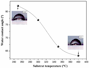
Figure 7 shows the variation of the water contact angles for different deposited temperature. We notice that the contact angle decreases from 82.20° to 63.26° with 250°C to 400°C, respectively. The experimentally measured contact angle values of our films are less than 90° writes the hydrophilicity. The variation of the contact angle as a function TS is probably due to the size of the available pores, to the radius of the pores and/or to their distribution [30-32]. In addition, this behavior could be attributed to the effect of the density of the layers, method of thin films preparation [33] and the size of the crystallite. The small value of water contact angle for 400℃ is due to the high value of the crystallite size (Table 1) and/or to the radius of the pores.
Figure 7. Variation of the water contact angles of ZnO thin films for different deposited temperature
Figure 8 shows the change in the electrical conductivity (σ) of ZnO films vs. TS. It is found that the conductivity increases with the increase of the substrate temperature. The conductivity of ZnO films prepared at 250℃, 300℃, 350℃ and 400℃ substrate temperature are 0.025 (Ω.cm)-1, 0.062 (Ω.cm)-1, 0.425 (Ω.cm)-1 and 1.033 (Ω.cm)-1, respectively. This augmentation in conductivity may be due to the appearance of zinc atoms in the interstitial site or the oxygen vacancies. This phenomenon has been found by other works in the literature [11, 17, 34].
The minimum value of conductivity (σ = 0.025 (Ω.cm)-1) for the film deposited at a substrate temperature of 250°C was mainly caused by the amorphous film structure (Figure 2). It is well known that these defects behave like donors, which induces an increase in the concentration of free carriers mainly electrons. With the increase of the substrate temperature, the film network is reorganized, which is accompanied by the reduction of structural defects. These results are strongly confirmed by the Urbache energy (Figure 6), which indicates that the disorder decreases with the increase of the substrate temperature that is the reorganization of the atoms in the films. Furthermore, the increase of the electrical conductivity with the substrate temperature can be due to the increase of the size crystallites in the films and consequently to the mobility of the carriers. So, the conductivity increases by the growth of the mobility of the electrons [35]. Minami et al. [36] attributed the increase in conductivity with increasing substrate temperature is due to the improvement in film crystallinity. It is interesting to note that the best value of the electrical conductivity obtained in this work (σ = 1.033 (Ω.cm)-1) is high than that obtained by the spray pyrolysis technique (σ = 0.390(Ω.cm)-1) [14] for the TS = 400℃.
Figure 8. Evolution of the electrical conductivity of the ZnO thin films as a function of TS
The study of structural, optical and electrical properties by varying the substrate temperature. DRX analysis indicates that our films have a wurtzite structure, with a preferential orientation (100) for TS = 300℃ to 400℃. In addition, a steep transition in the microstructure of ZnO passing from an amorphous structure to a crystalline structure for a temperature equal to 300℃. D increase with increasing of the substrate temperature. An improvement in the transmittance of 65% to 82% with a decrease of Eg (3.34 to 3.21 eV) depending to TS according to the increase of D. The decrease in EU vs. TS indicating a decrease in defects. The measured contact angles are less than 90° for all the prepared samples confirming the hydrophilic character of all the films. An improvement in electrical conductivity by increasing these values as a function of deposited temperature. According to these results, the layer deposited at 400℃ exhibits better crystalline quality with excellent optical and electrical properties can be used as promising candidates in opto-electronic device applications.
This work is supported by the Research Project University-Formation (PRFU) of Algeria (N°. A10N01UN280120180005) entitled “Study, elaboration and characterization of (CZTS, SnS) absorbers films and (ZnO, SnO2) TCO materials for photovoltaic applications”.
[1] Vittal, R., Ho, K.C. (2017). Zinc oxide based dye-sensitized solar cells: A review. Renewable and Sustainable Energy Reviews, 70: 920-935. https://doi.org/10.1016/j.rser.2016.11.273
[2] Daranfed, W., Guermat, N., Bouchama, I., Mirouh, K., Dilmi, S., Saeed, M.A. (2019). Effect of the deposition times on the properties of ZnO thin films deposited by ultrasonic spray pyrolysis for optoelectronic applications. Journal of Nano- and Electronic Physics, 11(6): 06001-06005. http://doi.org/10.21272/jnep.11(6).06001
[3] Anta, J.A., Guillén, E., Tena-Zaera, R. (2012). ZnO-based dye-sensitized solar cells. Journal of Physical Chemistry C, 116(21): 11413-11425. http://dx.doi.org/10.1021/jp3010025
[4] Galstyan, V., Comini, E., Baratto, C., Faglia, G., Sberveglieri, G. (2015). Nanostructured ZnO chemical gas sensors. Ceramics International, 41(10): 14239-14244. https://doi.org/10.1016/j.ceramint.2015.07.052
[5] Arakelova, E., Khachatryan, A., Kteyan, A., Avjyan, K., Grigoryan, S. (2016). ZnO film deposition by DC magnetron sputtering: Effect of target configuration on the film properties. Thin Solid Films, 612: 407-413. https://doi.org/10.1016/j.tsf.2016.06.030
[6] Znaidi, L. (2010). Sol–gel-deposited ZnO thin films. Materials Science and Engineering B, 174(1-3): 18-30. http://dx.doi.org/10.1016/j.mseb.2010.07.001
[7] Wang, S., Chen, M., Zhao, K., Yu, W., Chen, J., Zhao, S., Wang, J., Fu, G. (2011). Laser-induced lateral voltage in epitaxial Al-doped ZnO thin films on tilted sapphire. Applied Physics A, 103: 1179-1182. https://doi.org/10.1007/s00339-010-6106-1
[8] Kumari, N., Patel, S.R., Gohel, J.V. (2018). Optical and structural properties of ZnO thin films prepared by spray pyrolysis for enhanced efficiency perovskite solar cell application. Optical and Quantum Electronics, 50: 180. https://doi.org/10.1007/s11082-018-1376-5
[9] Benramache, S., Rahal, A., Benhaoua, B. (2014). The effects of solvent nature on spray-deposited ZnO thin film prepared from Zn (CH3COO)2, 2H2O. Optik, 125(2): 663-666. https://doi.org/10.1016/j.ijleo.2013.07.085
[10] Rahal, A., Benramache, S., Benhaoua, B. (2014). Substrate temperature effect on optical property of ZnO thin films. Engineering Journal, 18(2): 81-88. https://doi.org/10.4186/ej.2014.18.2.81
[11] Benramache, S., Benhaoua, B. (2012). Influence of substrate temperature and Cobalt concentration on structural and optical properties of ZnO thin films prepared by Ultrasonic spray technique. Superlattices and Microstructures, 52(4): 807-815. http://dx.doi.org/10.1016/j.spmi.2012.06.005
[12] Ashour, A., Kaid, M.A., El-Sayed, N.Z., Ibrahim, A.A. (2006). Physical properties of ZnO thin films deposited by spray pyrolysis technique. Applied Surface Science, 252(22): 7844-7848. https://doi.org/10.1016/j.apsusc.2005.09.048
[13] Mahmood, A., Ahmed, N., Raza, Q., Khan, T.M., Hassan, M.M., Mahmood, N. (2010). Effect of thermal annealing on the structural and optical properties of ZnO thin films deposited by the reactive e-beam evaporation technique. Physica Scripta, 82(6): 1-8. https://doi.org/10.1088/0031-8949/82/06/065801
[14] Zahedi, F., Dariani, R.S., Rozati, S.M. (2013). Effect of substrate temperature on the properties of ZnO thin films prepared by spray pyrolysis. Materials Science in Semiconductor Processing, 16(2): 245-249. http://dx.doi.org/10.1016/j.mssp.2012.11.005
[15] Zhao, Y., Jiang, Y., Fang, Y. (2007). The influence of substrate temperature on ZnO thin films prepared by PLD technique. Journal of Crystal Growth, 307(2): 278-282. https://doi.org/10.1016/j.jcrysgro.2007.07.025
[16] Li, X.H., Huang, A.P., Zhu, M.K., Xu, S.L., Chen, J., Wang, H., Wang, B., Yan, H. (2003). Influence of substrate temperature on the orientation and optical properties of sputtered ZnO films. Materials Letters, 57(30): 4655-4659. https://doi.org/10.1016/S0167-577X(03)00379-3
[17] Karakose, E., Çolak, H. (2017). Effect of substrate temperature on the structural properties of ZnO nanorods. Energy, 141: 50-55. https://doi.org/10.1016/j.energy.2017.09.080
[18] Kang, S.J., Joung, Y.H. (2007). Influence of substrate temperature on the optical and piezoelectric properties of ZnO thin films deposited by rf magnetron sputtering. Applied Surface Science, 253(17): 7330-7335. https://doi.org/10.1016/j.apsusc.2007.03.020
[19] Volintiru, I., Creatore, M., Linden, J.L., van de Sanden, M.C.M. (2006). Expanding thermal plasma-deposited ZnO films: Substrate temperature influence on films properties: Film growth studies. Superlattices and Microstructures, 39(1-4): 348-357. https://doi.org/10.1016/j.spmi.2005.08.061
[20] Khalfallah, M., Guermat, N., Daranfed, W., Bouarissa, N., Bakhti, H. (2020). Hydrophilic nickel doped porous SnO2 thin films prepared by spray pyrolysis. Physica Scripta, 95(9): 095805. https://doi.org/10.1088/1402-4896/aba8c5
[21] Guendouz, H., Bouaine, A., Brihi, N. (2018). Biphase effect on structural, optical, and electrical properties of Al-Sn codoped ZnO thin films deposited by sol-gel spin-coating technique. Optik, 158: 1342-1348. https://doi.org/10.1016/j.ijleo.2018.01.025
[22] Chou, H., Yang, M.S., Wu, C.P., Tsao, Y.C., Chen, B.J., Liao, T.F., Sun, S.J., Chiou, J.W. (2011). Extended wide band gap amorphous aluminium-doped zinc oxide thinfilms grown at liquid nitrogen temperature. Journal of Physics D: Applied Physics, 44(20): 1-7. https://doi.org/10.1088/0022-3727/44/20/205404
[23] Evstropiev, S.K., Gatchin, Y.A., Evstropyev, K.S., Romanova, E.B. (2016). Spectral properties of ZnO and ZnO-Al2O3 coatings prepared by polymer-salt method. Optical Engineering, 55(4): 1-5. https://doi.org/10.1117/1.OE.55.4.047108
[24] Aoun, Y., Benhaoua, B., Benramache, S., Gasmi, B. (2015). Effect of annealing temperature on structural, optical and electrical properties of zinc oxide (ZnO) thin films deposited by spray pyrolysis technique. Optik, 126(24): 5407-5411. http://dx.doi.org/10.1016/j.ijleo.2015.08.267
[25] Daranfed, W., Guermat, N., Mirouh, M. (2020). Experimental study in the effect of precursors in Co3O4 thin films used as solar absorbers. Annales de Chimie - Science des Matériaux, 44(2): 121-126. https://doi.org/10.18280/acsm.440207
[26] Belkhalfa, H., Ayed, H., Hafdallah, A., Aida, M.S., Tala Ighil, R. (2016). Characterization and studying of ZnO thin films deposited by spray pyrolysis: Effect of annealing temperature. Optik, 127(4): 2336-2340. http://dx.doi.org/10.1016/j.ijleo.2015.11.126
[27] Younggyu, K., Youngbin, P., Jae-Young, L. (2017). Influence of annealing temperature on band gap shift and optical constants of al-doped ZnO thin films deposited on muscovite mica substrates. Journal of Nanoscience and Nanotechnology, 17(8): 5566-5569. https://doi.org/10.1166/jnn.2017.14142
[28] Daranfed, W., Aida, M.S., Attaf, N., Bougdira, J., Rinnert, H. (2012). Cu2ZnSnS4 thin films deposition by ultrasonic spray pyrolysis. Journal of Alloys and Compounds, 542: 22-27. http://dx.doi.org/10.1016/j.jallcom.2012.07.063
[29] Zhang, R., Hummelgard, M., Olin, H. (2014). A facile one-step method for synthesising a parallelogram-shaped single- crystalline ZnO nanosheet. Materials Science and Engineering: B, 184: 1-6. http://dx.doi.org/10.1016/j.mseb.2013.12.009
[30] Guermat, N., Bellel, A., Sahli, S., Segui, Y., Raynaud, P. (2009). Thin plasma-polymerized layers of hexamethyldisiloxane for humidity sensor development. Thin Solid Films, 517(15): 4455-4460. https://doi.org/10.1016/j.tsf.2009.01.084
[31] Guermat, N. (2017). Elaboration and modeling of water molecule sensitive layers deposited from hexamethyldisiloxane. Advanced Structured Materials, 33: 315-324. https://doi.org/10.1007/978-981-10-1602-8_26
[32] Guermat, N., Bellel, A., Sahli, S., Segui, Y., Raynaud, P. (2014). Plasma Polymerization of hexamethyldisiloxane and tetraethoxysilane thin films for humidity sensing application. Defect and Diffusion Forum, 354: 41-47. https://doi.org/10.4028/www.scientific.net/DDF.354.41
[33] Eskandari, A., Sangpour, P., Vaezi, M.R. (2014). Hydrophilic Cu2O nanostructured thin films prepared by facile spin coating method: Investigation of surface energy and roughness. Materials Chemistry and Physics, 147(3): 1204-1209. http://dx.doi.org/10.1016/j.matchemphys.2014.07.008
[34] Zaier, A., Oum El az, F., Lakfif, F., Kabir, A., Boudjadar, S., Aida, M.S. (2009). Effects of the substrate temperature and solution molarity on the structural opto-electric properties of ZnO thin films deposited by spray pyrolysis. Materials Science in Semiconductor Processing, 12(6): 207-211. https://doi.org/10.1016/j.mssp.2009.12.002
[35] Khan, M.I., Bhatti, K.A., Qindeel, R., Bousiakou, L.G., Alonizan, N., Aleem, F. (2016). Investigations of the structural, morphological and electrical properties of multilayer ZnO/TiO2 thin films deposited by sol-gel technique. Results in Physics, 6: 156-160. http://dx.doi.org/10.1016/J.rinp.2016.01.015
[36] Minami, T., Sato, H., Ohashi, K., Tomofuji, T., Takata, S. (1992). Conduction mechanism of highly conductive and transparent zinc oxide thin films prepared by magnetron sputtering. Journal of Crystal Growth, 117(1-4): 370-374. https://doi.org/10.1016/0022-0248(92)90778-H