Experimental Study of Precursor Concentration the Co3O4 Thin Films Used as Solar Absorbers

Warda Daranfed* | Noubeil Guermat | Kamel Mirouh
© 2020 IIETA. This article is published by IIETA and is licensed under the CC BY 4.0 license (http://creativecommons.org/licenses/by/4.0/).
OPEN ACCESS
The objective of this work is to develop Co3O4 films and to investigate the influence of different precursor concentration on the structural, morphological, optical and electrical properties of Co3O4 thin films, in order to improve the optoelectronic properties of these films. Finally, we have developed thin films of Co3O4 at different precursor concentrations (0.05 to 0.15 mol/l) under a substrate temperature set to 400°C and 4 minutes as deposition time. XRD analysis has shown that the deposited layers have a cubic spinel structure with a preferential orientation along the direction (311). The morphological studies have shown that the surface morphology of the films was almost homogeneous and dense. The presence of the peaks associated with the Co and O elements, which were present in the EDS analysis, confirmed the composition of the films. The optical characterization of our film has shown a low transmittance (from 16 to 0.9%) in the visible region and the IR region varies between 40 to 2% over the range of precursor concentration varied between 0.05 and 0.125 mol/l and a high absorbance of the order of 100% for the film deposit of 0.15 mol/l. The obtained gap values are ranged from 1.44 to 1.52 eV and 2.05 to 2 eV for lower and higher energy regions in the range of precursor concentration 0.05–0.125 mol/l. The film prepared at 0.15 mol/l, had a good p-type electrical semiconductor and good absorbance of sunlight.
thin film, Co3O4, precursor concentration, spray pyrolysis, XRD, transmittance
Converting solar energy into electricity is an attractive alternative to fossil fuels. Among some solar absorber materials and semiconductors used for the production of photovoltaic cells, silicon, which is an element abundant despite its indirect gap, is still the most commonly used not only because of its conversion efficiency but also for its non-toxicity. The next generation of photovoltaic systems may consist of thin layers of metal oxide-based absorbent and transparent conductors. The n-type semiconductor oxides, such as; ZnO, ITO, TiO2 as TCOs, are often used [1-3]. The p-type semiconductor oxide is generally limited to Cu2O [4, 5]. Therefore, the development of a photovoltaic cell "all oxide" is very interesting to produce at low cost and large-scale solar cells. The oxides, having the type spinel structure, are among the best candidates to replace Cu2O as a p-type semiconductor for photo absorption application, including photovoltaics. This has been shown in tests performed on the efficiency of new solar cells "all oxide" including materials being studied. The spinel oxides are attractively absorption in the UV-VIS region. Theoretical studies provide a low value of optical band gap (Eg ~ 0.5 eV) corresponding to the transition cation-cation in the octahedral sites with a direction spin-up compared to Cu2O [4]. Recently, the interest has focused on the oxide spinel of the formula Co3O4, which is a p-type semiconductor and light absorbent. It consists of an abundant and chemically stable element and has all the essential characteristics for the photovoltaic application. This oxide has two notable direct transitions in the visible range with a bandgap energy of 1.45 eV et 2.26 eV [6], it has a spinel structure of AB2O4 type; where the Co2+ ions occupy the tetrahedral sites 8a and Co3+ occupy the octahedral sites 16d [7]. Thin films can be prepared by various techniques such as PVD (physical vapor deposition) [8], CVD (chemical vapor deposition) [9]. Among these techniques the spray pyrolysis technique has many advantages such as low cost, easy to manipulate, convenient for large area deposition, uniform film deposition and allows the possibility to obtain a thin layers of Co3O4 with the properties required for different applications such as: solar selective absorbers [10], anodic electrochromic materials in smart window devices [11], negative electrodes in lithium-ion batteries [12] rechargeable batteries, sensing, protective layers or pigment for glasses, ceramics. The objective of this work is to combine, by the spray pyrolysis technique, light-absorbing semiconductor and spinel oxide nanoparticles (Co3O4). Different substitutions will modulate physical characteristics such as energy gap, light absorption and resistivity for different applications, including for photovoltaics.
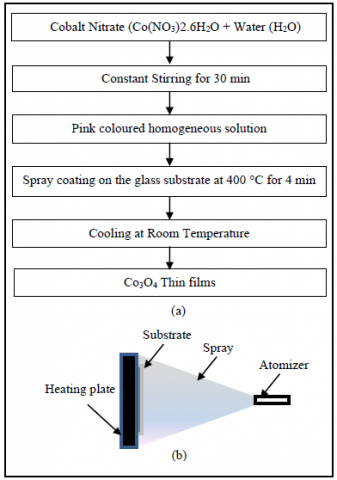
Co3O4 films were prepared on glass substrates using a spray pyrolysis technique (Figure 1). The spray solution changed from 0.05 to 0.15 mol/l, while (Co(NO3)2 6H2O) (cobalt nitrate) diluted in distilled water. The choice of distilled water is due to its abundance and low cost. An addition of a few drops of hydrochloric acid is necessary to ensure maximum dissolution of (Co(NO3)2 6H2O). The mixture solution was stirred at room temperature for 30 min to obtain homogeneous solution, and the deposition time was 4 min. For the prepared sets, the distance between atomizer and substrate is fixed at 22 cm. The carrier gas (compressed air) and solution were fed into a spray nozzle at a pre-adjusted constant atomization pressure and the substrate temperature was held constant at 400°C. The structural properties were determined by XRD using a Philips X’ Pert system with Cu Kα radiation ((λCuKα = 1.5418 Å). the morphology and composition of the film were analyzed using a microscopic scanning SEM equipped with an EDX analysis system. The optical transmission was in the UV–visible range of (300–1000 nm); the measurements were performed using Shimadzu UV–3101 PC spectrophotometer and Hall Effect for electrical properties.
Figure 1. (a) Flow diagram for deposition of Co3O4 thin and (b) films Schematic diagram of spray pyrolysis equipment
3.1 Structural and morphology properties
Figure 2 shows the diffraction patterns of X-ray film Co3O4 as a various precursor concentration. From Figure 1, we notice the presence of peaks (111) (220) (311) (400) (422) (511) and (440) relating to Co3O4 material, located at angles 18.90°, 31.30°, 36.81°, 44.90°, 55.70°, 59.50° and 64.92º respectively. Following the JCPD standard files (JPPDS no.42–1467), the peaks found assigned to the Spinel type Cubic structure. The same result was reported in several studies [13, 14]. We notice that, the most intense peak for our films was at a preferred orientation according to the plan (311). This preferential growth orientation is often observed in other studies [14]. It is clear is that the intensity and the refinement of this peak increase with increasing molar concentration, so we can conclude that the increase in molar concentration improves the crystallinity of the material. The results found are in perfect agreement with the work of Patel et al. [15], where the prepared Co3O4 films have different thicknesses (from 70 nm to 230 nm) on the FTO substrate by sputtering. Hamdani et al. [16], who prepared thin films of Co3O4 by the spray pyrolysis technique found a preferential orientation according to the plan (311) and obtained a single phase for the films of Co3O4, while Avila et al. [13] observed the appearance of some secondary phases corresponding to CoO and Co2O3.
Figure 2. XRD patterns of Co3O4 films for different precursor concentrations
From the diffractograms X-ray, it is possible to deduce the average crystallite size using Scherrer's formula 1 [17]:
${{D}_{(hkl)}}=\frac{K\lambda }{\beta \cos \theta }$ (1)
where, D(hkl) is the mean diameter of the crystallites in a direction normal to the family of planes (hkl), k is the form factor (it is worth 0.9 for isotropic or quasi-isotropic crystallites), θ is the wavelength of the X-ray source, (hkl) is the diffraction angle of the line (hkl), β is the full width at half maximum.
To calculate values (ε) of Co3O4 film along the plane (311) were calculated using the following formula [18]:
$\varepsilon =\frac{\beta \cos \theta }{4}$ (2)
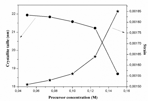
Figure 3 shows the variation of the crystallite size and strain for the Co3O4 films prepared at different precursor concentrations. An inverse relationship between the variation of the crystallite size and the strain can be noticed. Note that the crystallite size values decrease with the increase of the solution molarity. We can interpret the decrease in crystallites size (degradation of crystal quality) by the increase in nucleation centers with the increase in precursor concentration; these results are comparable with those of other authors [19].
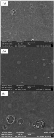
The surfaces of our films were analyzed by scanning electron microscopy (SEM). The SEM images of Co3O4 films deposited by spray pyrolysis with three molarities of 0.05 mol/l, 0.075 mol/l and 0.15 mol/l are shown in Figures 4 (a, b, and c). In all cases, it can be seen that the film surfaces have a uniform and compact appearance with the formation of bubbles on the surface and for the film prepared with low molar concentration, the surface contains pores (Figure 4 b). On the other hand, with the increase in precursor concentration, the pores disappeared and the increase in bubbles for the film deposited with a high molar concentration (Figure 4 c) can be related to the increase in film thicknesses.
Figure 3. The variation of crystallite size and strain as a function of precursor concentration of Co3O4 thin films
Figure 4. SEM images for Co3O4 films deposited with: (a) 0.05 mol/l, (b) 0.075 mol/l and (c) 0.15 mol/l
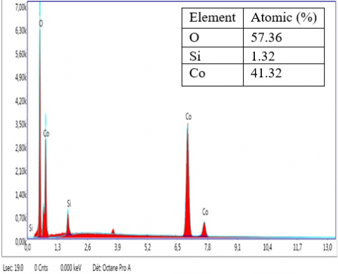
In Figure 5 we have reported the typical EDS spectra for the deposited film Co3O4 with 0.15 mol/l at substrate temperature equal to 400°C. It is evident from spectra, the presence of two Co and O elements constituting the film and the presence of other elements in the spectrum originated from the substrate glass (Si). In addition, the O: Co ratio is equal to 1.34 for the films deposited with 0.15 mol/l, which is equal to the ideal value [20].
Figure 5. Typical EDS spectra for the deposited film Co3O4 with the molar concentration
3.2 Optical properties
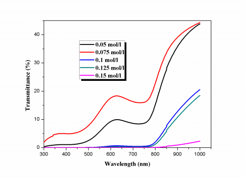
Due to the thickness, the films prepared in low molar concentration varying between 0.05 and 0.075 mol/l have a higher transmittance in the infrared region (IR) and small values of transmittance in the visible region. Indeed, a low molar concentration leads to thinner layers for the same deposition time (in our case 4 minutes). On the other hand, the films prepared with a molar concentration greater than or equal to 0.1 mol/l have a low transmittance in the visible range (T ≤ 0.5 %) (Figure 6) with the presence of two absorption bands in the spectra of transmittance, in which, the first is in the visible region with a wavelength equal to 570 nm and the second in the infrared region with a wavelength of 810 nm (Figure 6) for molar concentration range from 0.05 mol/l to 0.125 mol/l. Films deposited with a higher molar concentration (Molarity ≤ 0.15 mol/l) are completely absorbing radiation in the visible range (400-600 nm). From this result, we can confirm the presence of two direct gaps, which agree with other studies in the literature [21, 22]. On the other hand, for a molar concentration equal to 0.15 mol/l there is a single absorption band located in the infrared region that corresponds to one optical gap.
Figure 6. Transmittance spectra of Co3O4 films for different precursor concentrations
From the transmittance spectra, we deduced the optical gap Eg of our films from the following formula:
${{\left( \alpha h\nu \right)}^{n}}=B\left( h\nu -{{E}_{g}} \right)$ (3)
where, B is a constant, Eg is the bandgap of the semiconductor and n a constant equal to 2 for indirect gap and 0.5 for the direct gap compounds [1]. The band gap energies are then obtained by extrapolating the linear portion of (αhυ)2 versus (hυ) plots to the energy axis at (αhv)2 = 0.
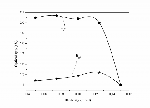
As we can see in Figure 6, the values of the optical gaps Eg1 and Eg2 varying from 1.44 to 1.52 eV and from 2.05 to 2 eV respectively, and these values agree with the literature [22, 23]. The values of the first gap are generally associated with a charge transfer (O-2 → Co+3) while the values of the second gap are associated with the charge transfer (O-2 → Co+2) [24, 25]. We also note the existence of an inverse variation between the two gaps (Figure 7) i.e. the augmentation of Eg1 is accompanied by a reduction of Eg2. This reduction improves the value of the gap to approach the desired value for photovoltaic applications [12].
The absorption coefficient of films shows a tail for sub-bandgap photon energy. This tail called the Urbach tail. The latter, which is closely related to the disorder in the film network, is expressed as [17]:
$\alpha ={{\alpha }_{0}}\exp \frac{h\nu }{{{E}_{0}}}$ (4)
where, α0 is a constant and Ε0 is interpreted as the width of the tails of localized states in the gap region. To evaluate the values of α0 and Ε0, one has to plot the variation of absorption coefficient α in logarithmic scale as a function of photon energy hν.
As it can be seen from the Figure 8, the variation of optical band gap increases from 1.44 to 1.52 eV with the increase of the precursor concentration from 0.05 to 0.125 mol/l and decrease to 1.40 eV for precursor concentration equal to 0.15 mol/l. However, films prepared at precursor concentration of 0.15 mol/l have an optical band gap close to 1.4 eV required for solar cells since it matches well with solar spectrum. This variation can be related to the variation of the disorder in films, a decrease in the disorder is observed, this decrease is due to a slow growth rate, incoming species on the substrate surface have enough time to find a suitable site and to form a more organized material. On the contrary, the increase in the disorder is due to the higher growth rate, which leads to a very disordered network due to the rapid film formation. A reduction in the band tail width is followed by the increase in the optical bandgap. This suggests that the variation of the optical gap is governed by the disorder in the film network.
Figure 7. Variation of the optical gaps of Co3O4 films at different precursor concentration
Figure 8. Variation of the optical band gap and disorder in film network as a function of the molar concentration
3.3 Electrical properties
The film's electrical resistivity was characterized by the mean of Hall Effect measurements in order to determine the resistivity, free carriers’ concentration, and mobility. In Table 1, we have reported the electrical resistivity and free carriers’ concentration of the deposited Co3O4 thin films. It can be seen that; the electrical resistivity follows faithfully the trend of the carriers’ concentration. This indicates clearly that the resistivity is rather controlled by the free carrier concentration. We noticed that the resistivity values are comparable to that given by other authors [12, 26]. The whole prepared films have p type conductivity according to Hall's constant sign. As we can correlate this variation in resistivity with the degree of crystallization which, in our analysis by XRD, is translated by the evolution of the crystallite size. Therefore, there are more grain boundaries that are a limiting factor of μ. On the other hand, the increase in resistivity is due to the increase in the particles of cobalt (Co+3) with molar concentration. This generates a reduction in the holes of the latter, which are responsible for the electrical conduction by hopping. The same result is observed by Cheng et al. [27] have deposited Co3O4 thin films by chemical vapour deposition. The film deposition for the substrate temperature change from 200 to 400 K produces a resistivity increase in the hopping conduction between Co+2 and Co+3 (the conduction of the films was confined to be due to polaronic hopping of holes). We concluded that the conductivity is controlled by the free carrier concentration more than by its mobility. In addition, the spray pyrolysis deposited Co3O4 films have electrical resistivity better than the previous results [28].
Table 1. Electrical resistivity, carriers concentration, and mobility with different precursor concentration of Co3O4
|
Sample, (mol/l) |
Resistivity ρ, (Ω.cm) |
μ (cm2V-1 S-1) |
Free carrier concentration N, (cm)-3 |
Thickness d, (nm) |
|
0.05 0.075 0.1 0.125 0.15 |
1.691 1.091 1.616 6.186 7.450 |
30.03 15.03 26.63 69.70 179.90 |
2.701 ×10¹⁶ 3.808 ×10¹⁸ 1.468 ×10¹⁷ 3.730 ×10¹⁶ 4.761 1015 |
564 450 1163 1780 2300 |
The objective of this study was to investigate the influence of the precursor concentration of the structural, microstructural, optical and electrical thin films of Co3O4 to improve the optoelectronic properties of the latter. The results obtained from the characterization by X-ray diffraction on the deposited films have shown that the films based on Co3O4 are polycrystalline, with a preferential orientation along the plane (311) which corresponds to the direction of the cubic structure the Spinel type. The increase in precursor concentration is accompanied by an increase in the intensity of the diffraction peak (31I). The morphological study of the films by SEM has shown that, for a low precursor concentration, the elaborated film is smooth, homogeneous, dense and contains pores, that disappears with the increase in molar concentration. The optical characterization of our layers has shown a low transmission varies varying from 4% to 17% in the visible region and between 45% and 14% for the IR region for precursor concentration varying between 0.05 mol/l and 0.125 mol/l, and a high absorbance of the order of 100% for precursor concentration of 0.15 mol/l. The obtained gap values vary from 1.462 eV to 1.48 eV and 2.09 eV to 2.03 eV respectively for the precursor concentration changes between 0.05 to 0.125 mol/l and equal 1.4 for molar concentration of 0.15 eV. The electrical resistivity of the prepared films increases with molar concentration from 1.691 to 7.450 (Ω.cm). Finally, and from the results obtained during the characterizations process, it can be concluded that the optimal precursor concentration for technological applications such as the absorbent layer in the solar cells is 0.15 mol/l.
[1] Daranfed, W., Guermat, N., Bouchama, I., Mirouh, K., Dilmi, S., Saeed, M.A. (2019). Effect of the deposition times on the properties of ZnO thin films deposited by ultrasonic spray pyrolysis for optoelectronic applications. Journal of Nano- and Electronic Physics, 11(6): 06001-06005. http://doi.org/10.21272/jnep.11(6).06001
[2] Sholehah, A., Pusparasmi, D.A., Yuliarto, B. (2019). The application of zinc oxide layer as ethylene sensor. International Seminar on Metallurgy and Materials, 541: 01-05. https://doi:10.1088/1757-899X/541/1/012051
[3] Hitosugi, T., Yamada, N., Nakao, S., Hirose, Y., Hasegawa, T. (2010). Properties of TiO2-based transparent conducting oxides. Phys. Status Solidi A, 207(7): 1529–1537. http://doi.org/10.1002/pssa.200983774
[4] Brandt, I.S., Martins, C.A., Zoldan, V.C., Viegas, A.D.C., Dias da Silva, J.H., Pasa, A.A. (2014). Structural and optical properties of Cu2O crystalline electrodeposited films. Thin Solid Films, 562: 144-151. http://doi.org/10.1016/j.tsf.2014.04.013
[5] Chudy, P.S., Sibinski, M., Pawełek, R., Wisz, G., Cieniek, B., Potera, P., Szczepan, P., Adamiak, S., Cholewa, M., Głowa, L. (2019). Characteristics of TiO2, Cu2O, and TiO2/Cu2O thin films for application in PV devices. AIP Advances, 9(5): 055206. https://doi.org/10.1063/1.5093037
[6] Barakat, N.A.M., Khil, M.S., Sheikh, F.A., Kim, H.Y. (2008). Synthesis and optical properties of two cobalt oxides (CoO and Co3O4) nanofibers produced by electrospinning process. The Journal of Physical Chemistry C, (112): 12225-12233. https://doi.org/10.1021/jp8027353
[7] Elenice dos Santos, M., Aparecido Ferreira, R., Noronha Lisboa-Filho, P., Pena, O. (2013). Cation distribution and magnetic characterization of the multiferroic cobalt manganese Co2MnO4 spinel doped with bismuth. Journal of Magnetism and Magnetic Materials, 329: 53-58. http://doi.org/10.1016/j.jmmm.2012.09.070
[8] Guyon, C., Barkallah, A., Rousseau, F., Giffard, K., Morvan, D., Tatoulian, M. (2011). Deposition of cobalt oxide thin films by plasma-enhanced chemical vapour deposition (PECVD) for catalytic applications. Surface & Coatings Technology, 206(7): 1673-1679. https://doi.org/10.1016/j.surfcoat.2011.09.060
[9] Burriel, M., Garciaa, G., Santiso, J., Hansson, A.N., Linderoth, S., Figueras, A. (2005). Co3O4 protective coatings prepared by pulsed injection metal organic chemical vapour deposition. Thin Solid Films, 473(1): 98-103. https://doi.org/10.1016/j.tsf.2004.07.081
[10] Kadam, L.D., Patil, P.S. (2001). Thickness-dependent properties of sprayed cobalt oxide thin films. Materials Chemistry and Physics, 68(1-3): 225-232. https://doi.org/10.1016/S0254-0584(00)00367-9
[11] Wang, L., Song, X.C., Zheng, Y.F. (2012). Electrochromic properties of nanoporous Co3O4 thin films prepared by electrodeposition method. Micro & Nano Letters, 7: 1026-1029. https://doi.org/10.1049/mnl.2012.0609
[12] Louardi, A., Rmili, A., Ouachtari, F., Bouaoud, A., Elidrissi, B., Erguig, H. (2011). Characterization of cobalt oxide thin films prepared by a facile spray pyrolysis technique using perfume atomizer. Journal of Alloys and Compounds, 509(37): 9183-9189. https://doi.org/10.1016/j.jallcom.2011.06.106
[13] Avila, A.G., Barrera, E.C., Huerta, L.A., Muhl, S. (2004). Cobalt oxide films for solar selective surfaces, obtained by spray pyrolisis. Solar Energy Materials & Solar Cells, 82(1-2): 269-278. http://doi.org/10.1016/j.solmat.2004.01.024
[14] Patil, V., Joshi, P., Chougule, M., Sen S. (2012). Synthesis and characterization of Co3O4 thin film. Soft Nanoscience Letters, 2(1): 1-7. https://doi.org/10.4236/snl.2012.21001
[15] Patel, M., Kim, J. (2018). Thickness-dependent photoelectrochemical properties of a semitransparent Co3O4 photocathode. Beilstein Journal of Nanotechnology, 9: 2432-2442. https://doi.org/10.3762/bjnano.9.228
[16] Hamdani, M., Pereira, M., Douch, J., Addi, A.A., Berghoute, Y., Mendonça, M.H. (2004). Physicochemical and electrocatalytic properties of Li-Co3O4 anodes prepared by chemical spray pyrolysis for application in alkaline water electrolysis. Electrochimica acta, 49(9-10): 1555-1563. https://doi.org/10.1016/j.electacta.2003.11.016
[17] Daranfed, W., Aida, M.S., Hafdallah, A., Lekiket, H. (2009). Substrate temperature influence on ZnS thin films prepared by ultrasonic spray. Thin Solid Films, 518(4): 1082-1084. https://doi.org/10.1016/j.tsf.2009.03.227
[18] Daranfed, W., Aida, M.S., Attaf, N., Bougdira, J., Rinnert, H. (2012). Cu2ZnSnS4 thin films deposition by ultrasonic spray pyrolysis. Journal of Alloys and Compounds, 542: 22-27. https://doi.org/10.1016/j.jallcom.2012.07.063
[19] Lakehal, A., Bouaza, A., Benrabah, B., Dalache, C., Benhebal, H. (2018). Characterization of Mn-doped Co3O4 thin films prepared by Sol Gel-Based Dip-coating process. High Temperature Materials and Processes, 38(2019): 1-11. https://doi.org/10.1515/htmp-2017-0185
[20] Dhas, C.R., Venkatesh, R., Kirubakaran, D.D., Merlin, J.P., Subramanian, B., Raj, A.M.E. (2017). Electrochemical sensing of glucose and photocatalytic performance of porous Co3O4 films by nebulizer spray technique. Materials Chemistry and Physics, 186: 561-573. https://doi.org/10.1016/j.matchemphys.2016.11.037
[21] Lekshmy, S.S., Joy, K. (2013). SnO2 thin films doped indium prepared by the sol-gel method: structure, electrical and photoluminescence properties. Journal of Sol-Gel Science and Technology, 67(1): 29-38. https://doi.org/10.1007/s10971-013-3047-0
[22] Barreca, D., Massignan, C., Daolio, S., Fabrizini, M., Piccirillo, C., Armelao, L., Tondello, E. (2001). Composition and microstructure of cobalt oxide thin films obtained from a novel cobalt(II) precursor by chemical vapor deposition. Chemistry of Materials, 13(2): 588–593. https://doi.org/10.1021/cm001041x
[23] Patil, P.S., Kadam, L.D., Lokhande, C.D. (1996). Preparation and characterization of spray pyrolysed cobalt oxide thin films. Thin Solid Films, 272(1): 29-32. https://doi.org/10.1016/0040-6090(95)06907-0
[24] Wang, X., Chen, X.Y., Gao, L.S., Zheng, H.G., Zhang, Z., Qian, Y.T. (2004). One-dimensional arrays of Co3O4 nanoparticles: Synthesis, characterization, and optical and electrochemical properties. The Journal of Physical Chemistry B, 108(42): 16401-16404. https://doi.org/10.1021/jp048016p
[25] Yamamoto, H., Tanaka, S., Hirao, K. (2003). Effects of substrate temperature on nanostructure and band structure of sputtered Co3O4 thin films. Journal of Applied Physics, 93(7): 4158–4162. https://doi.org/10.1063/1.1555681
[26] Kouidri, N., Rahmane, S., Allag, A. (2018). Substrate temperature-dependent properties of sprayed cobalt oxide thin films. Journal of Materials Science: Materials in Electronics, 30: 1153-1160. https://doi.org/10.1007/s10854-018-0384-3
[27] Cheng, C.S., Serizawa, M., Sakata, H., Hirayama, T. (1998). Co3O4 films prepared by chemical vapour deposition. Materials Chemistry and Physics, 53(3): 225-230. https://doi.org/10.1016/S0254-0584(98)00044-3
[28] Victoria, S.G., Raj, A.M.E., Ravidhas, G. (2015). An insight in the structural, morphological, electrical and optical properties of spray pyrolysed Co3O4 thin films. Materials Chemistry and Physics, 162: 852-859. https://doi.org/10.1016/j.matchemphys.2015.07.015