N Bharath Kumar* | Uma Maheswara Rao M | J. Veeranjaneyulu | Balapanur Mouli Chandra | P M Venkatesh
© 2024 The authors. This article is published by IIETA and is licensed under the CC BY 4.0 license (http://creativecommons.org/licenses/by/4.0/).
OPEN ACCESS
As the power quality problems emerge, the cost of fossil fuels rises and, in this case, the system requires a high energy storage device, which is effective, reliable and durable. In this study, a Superconducting Magnetic Energy Storage (SMES) device is utilized, that stores large amount of electrical power in superconducting coil and the energy stored, which is in the form of a DC magnetic field. The output attained from the SMES is AC, which is converted into DC with the aid of a 1-Ф PWM rectifier. To boost the operation, an input inductance is connected at the AC side and to smooth the DC voltage, an output capacitance is connected at the DC side in the PWM rectifier circuit. The PI controller is utilized to regulate the PWM rectifier and the parameters such as proportional constant (Kp) and integral constant (Ki) are tuned with the utilization of particle swarm optimization (PSO) algorithm, which provides best optimal values. The attained value is then fed to the grid through 1-Ф VSI, and the gating pulses for VSI are produced by comparing actual value with reference value that converts the DC into AC voltage. Thus, the grid synchronization and the compensation of reactive power are achieved with the aid of PI controller.
SMES, PSO algorithm, PWM rectifier, grid synchronization, PI controller, single phase VSI
The emissions from greenhouse gas and the pollution from fossil fuel are minimized with the usage of renewable energy, when compared this with the fossil fuel energy; the renewable energy is not stable. As a result of fluctuating renewable energy power, the grid power oscillations occur. To reduce these power oscillations on grid, energy storage is required to stable the output from the renewable energy [1]. There are many energy storage devices are required to reduce the power fluctuations on grid such as battery energy storage systems (BESS), pumped storage hydroelectric systems, and superconducting magnetic energy storage (SMES) systems. With the usage of BESS, it has short life span, reduces the ratings of voltage and current. With the usage of pumped hydroelectric systems, the size of the battery is big and topographic [2]. With the utilization of BESS, the reliability and power quality of the grid are improved, but in grid tied BESS, the conversion efficiency is lower because of losses in the DC-DC converter [3]. Normally, a high temperature superconducting (HTS) inductor is utilized to store and discharge the electric energy to the load, but when analogized this with the BESS, the response for SMES is fast [4]. The power oscillation is an inevitable issue in a microgrid that is powered by wind and PV energy sources, which is rectified with the utilization of SMES [5].
To minimize the coil size and improve the energy density, a high magnetic flux density is commonly utilized in superconducting SMES coil design. Due to continuous charging and discharging of SMES, there is no degradation in its performance [6]. With the utilization of SMES on a smart grid, the battery’s life and charging efficiency increases, which provides real and reactive power with a fast response to compensate the voltage [7]. The PV based microgrid transient faults are eradicated with the aid of SMES [8]. In this study, SMES is utilized which gives AC supply to the PWM rectifier to achieve grid synchronization. With the utilization of diode rectifier, the input current harmonics increases due to their inherent non-linear switching operation, which results serious power system issues [9] and [10]. A multi-pulse rectifier is utilized which is linked with phase-shifting transformer on the output side, through this method the harmonics are reduced, but the system is complex with the usage of large phase- shifting transformer [11]. With the increased number of pulses, the complexity of phase shift transformer increases which is connected in multi-pulse diode bridge rectifier [12]. The above mentioned drawbacks are eradicated with the utilization of PWM rectifier.
Conventionally PI controller is employed, which is simple to implement but it is not robust against the fluctuations in load and voltage of converters. Hence, it is overcome with the utilization of fuzzy logic controller (FLC), which is simple to learn but it takes long time to reach the steady state [13] and [14]. The above mentioned drawbacks are overcome with the aid of optimization technique like genetic algorithm (GA), which is utilized to tune the parameters of PI controllers. With the development of GA, the accuracy of the optimal solution and the convergence speed decreases [15]. In this study, a PSO algorithm is utilized which overcomes the drawbacks of existing algorithm.
In this present study, the SMES used in this system stores the electrical energy and the outcome of SMES is AC, which is fed to the PWM rectifier. A PSO based PI controller is utilized to control the PWM rectifier. To synchronize with the grid, the attained output is then fed to the grid through 1-Ф VSI and so the grid synchronization is achieved. The remaining parts describes the working of proposed control scheme, modelling of SMES, modelling of PWM rectifier, modelling of PSO based PI controller, modelling of 1-Ф VSI and Grid.
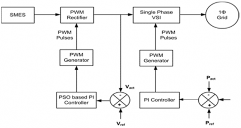
The proposed methodology contains SMES, which is an energy storage device that stores large amount of electric power. The stored energy is fed to the grid through 1Ф PWM rectifier, which is controlled with the aid of PSO based PI controller is illustrated in Figure 1.
The SMES used in this system stores the electric energy, which is in the form of DC magnetic field. The outcome of the SMES is AC, which is fed to the 1Ф PWM rectifier and the output attained from the PWM rectifier is DC voltage. With the utilization of PSO based PI controller, the gating pulses for the PWM rectifier are generated by comparing Vact with Vref values through which the rectifier is controlled. The attained DC voltage is fed to the grid through 1-Ф VSI, which is controlled with the aid of PI controller and the gating pulses for the VSI are generated by comparing Pact with Pref values and so the grid synchronization is achieved.
Figure 1. Proposed Control scheme
3.1 Modelling of SMES
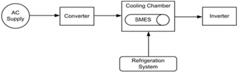
It is a type of energy storage system, which stores energy in a superconducting coil’s magnetic field. The DC flowing through the coil generates a magnetic field, which works at cryogenic temperature. The superconducting coil, ferromagnetic core, driving circuit and coolant are the major elements of SMES system. From these types, the superconducting coil, ferromagnetic core and coolant are utilized to hold or store the electric power and the driving circuit is utilized to inject or remove the electric power from SMES. The schematic structure of SMES is illustrated in Figure 2.
3.1.1 Superconducting coil
Because of coil’s ohmic resistance, the energy stored in an ordinary inductor or in a coil is impossible. The ohmic resistance has been eliminated from the coil, which decreases the conductor’s temperature and the conductor now known as superconductor. The superconductor’s characteristic feature is, it has the ability to carry high current with zero resistive elements. The quantity factor of the superconductor (QSC) determines the strength of the magnetic field and efficiency of the superconductor, which is expressed in Eq. (1). The superconductor’s quantity factor QSC is proportional to $E_m^{2 / 3}$, which depends on the constants r, a and Bm.
$Q_{S C}=5 \times 10^3\left(\frac{E_m^2}{B_m}\right)^{\frac{1}{3}} \times \frac{1}{\left\{\left(\frac{r}{a}-1\right)\left[\frac{r}{a}-\left(\frac{r^2}{a^2}-1\right)^{1 / 2}\right]^2\right\}^{1 / 3}}$ (1)
Figure 2. Schematic structure of SMES
3.1.2 Ferromagnetic core
The SMES’s storing capacity is increased by the ferromagnetic core within the superconducting coil, which stores lot of energy at lower current density. The volume inside and outside of the coil is occupied by the closed core arrangement, which avoids the leakage flux.
The maximum energy Em, stored in the coil is expressed in Eq. (2).
$\mathrm{E}_{\mathrm{m}}=\frac{1}{2} \mathrm{~L} I_m{ }^2 \approx \frac{1}{2} \mathrm{~B}_{\mathrm{s}} I_m \mathrm{NS}$ (2)
From Eq. (2), we know that the energy stored is due to the ferromagnetic core which is directly proportional to the induction of the core and the coil.
3.1.3 Driving circuit
The circuit layout of SMES comprises converter, DC-link capacitances, switches and varistor. The converter provides DC power to charge the SMES, while the charging and discharging states are controlled by the switches. The SMES is charged by turning ON the switches S1 and S4 and turning OFF the switches S2 and S3, whereas the SMES is discharged by turning ON the switches S2 and S3 and turning OFF the switches S1 and S4. On both the sides of input and output, two DC-link capacitances are utilized for rectification. The occurrence of over voltage in SMES is protected by using varistor and the inverter is utilized to supply power to the AC load.
3.1.4 Coolant
Due to the existence of small resistance in the conductor, the energy stored in the conductor is not possible and by lowering the temperature of the conductor, the resistance is detached, which is accomplished with the usage of coolant in SMES device. The SMES are categorized into high temperature superconductors (HTS) and low temperature superconductors (LTS) on the basis of coolant. Using the liquid nitrogen, the HTS is cooled at a temperature of 77°K, while using the liquid helium; the LTS is cooled at a temperature of 4.2°K. When comparing the liquid nitrogen with liquid helium, the liquid nitrogen is less expensive than the liquid helium. As a result, the liquid nitrogen is now utilized as a coolant in general in all industrial SMES, which works at high temperature with a maximum efficiency of cooling.
3.1.5 Mathematical formulation
During the charging conditions, the charging current I(t) at time t, is expressed as,
$\mathrm{I}(\mathrm{t})=\frac{\mathrm{U}}{\mathrm{L}} \mathrm{t}+\mathrm{I}_{\mathrm{o}}$ (3)
The voltage across the superconductor V(t), can be expressed as,
$\mathrm{V}(\mathrm{t})=\mathrm{L} \frac{\mathrm{dI}(\mathrm{t})}{\mathrm{dt}}$ (4)
The energy stored of the superconductor, E(t) at the time t, is expressed as,
$\mathrm{E}(\mathrm{t})=\frac{1}{2} \mathrm{LI}^2(\mathrm{t})$ (5)
During the discharging condition, the power supply P(t) to the load is constant,
$P(\mathrm{t})=\mathrm{U}^{\prime}(\mathrm{t}) \mathrm{I}^{\prime}(\mathrm{t})$ (6)
The current supply, I(t) at the time t, is expressed as,
$\mathrm{I}^{\prime}(\mathrm{t})=\sqrt{\mathrm{I}_{\mathrm{o}}^2-\frac{2}{\mathrm{~L}} \int \mathrm{p}^{\prime}(\mathrm{t}) \mathrm{dt}}$ (7)
The effective energy utilization factor, η which is expressed as,
$\eta=\frac{2 \mathrm{P}^{\prime} \mathrm{t}_{\mathrm{s}}}{\mathrm{LI}_{\mathrm{o}}^2}$ (8)
where, ts is written as,
$\mathrm{t}_{\mathrm{S}}=\frac{\frac{\mathrm{L}}{2}\left(\mathrm{I}_{\mathrm{o}}^2-\left(\mathrm{I}^{\prime}\right)^2\right)}{\mathrm{P}^{\prime}}$ (9)
The SMES supply constant power to the load up to the time ts, which is called as constant power discharging time. The output from the SMES is AC voltage, which is then fed to the PWM rectifier.
3.2 Modelling of single phase PWM rectifier
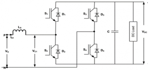
A Single Phase PWM rectifier used in this system contains four switches with an appropriate current carrying capacity, which converts the AC into DC voltage. To boost the operation, an input inductance is connected at the AC side and to smooth the DC voltage, an output capacitance is connected at the DC side in the PWM rectifier circuit. The circuit layout of PWM rectifier is illustrated in Figure 3.
Figure 3. Circuit layout of PWM rectifier
Under the condition of steady-state, assume the voltage supply, V_s as sinusoidal which is expressed as,
$V_s=j \omega L_s I_{s 1}+V_{c 1}$ (10)
where, the source current is denoted as Is1 and the voltage across the converter is denoted as Vc1.
With the help of PWM switching, the voltage across the converter is generated, which is expressed as,
$\mathrm{V}_{\mathrm{c}}=\mathrm{m}_{\mathrm{a}} \mathrm{V}_{\mathrm{dc}}$ (11)
where, the amplitude modulation index,
$\mathrm{m}_{\mathrm{a}}=\frac{\widehat{\mathrm{v}}_{\mathrm{sin}}}{\widehat{\mathrm{v}}_{\mathrm{tri}}}$ (12)
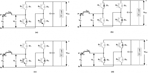
When the switch is turned ON, the inductance stores the energy and when the switch is turned OFF, the inductance discharges the energy to the output, and this is the working of DC boost chopper circuit. When the switch S2 is turned ON in the positive half cycle, the phase voltage is high. In this time, the input inductance stores the energy and the current is returned to the neutral through diode D4. When the switch S2 is turned OFF, the input inductance discharges the energy to the output through the diode D1 and then returned to the neutral through diode D4. The current paths at different switchin modes are illustrated in Figure 4.
Likewise, when the switch S4 is turned ON in the negative half cycle, the neutral voltage is high. In this time, the input inductance stores the energy and the current is returned to the phase through diode D2. When the switch S4 is turned OFF,the input inductance discharges the energy to the output through the diode D3 and then returned to the phase through diode D2. As a result, the energy stored in the inductor maximizes the DC bus voltage in both the positive and negative cycles and this circuit acts like a boost chopper. The working of boost, which is defined as follows, when the switch S2 is ON, the voltage across the capacitor Vc is zero and the corresponding voltage across the inductance, which is represented as,
$V_s=L_s \frac{d i_s}{d t}+V_c$ (13)
$\mathrm{V}_{\mathrm{s}}=\mathrm{L}_{\mathrm{s}} \frac{\mathrm{di}_{\mathrm{s}}}{\mathrm{dt}}=\mathrm{L}_{\mathrm{s}} \frac{\mathrm{I}_2-\mathrm{I}_1}{\mathrm{~T}_{\mathrm{on}}}$ (14)
$\mathrm{I}_2-\mathrm{I}_1=\frac{\mathrm{V}_{\mathrm{s}}}{\mathrm{L}_{\mathrm{s}}} \mathrm{T}_{\mathrm{on}}$ (15)
where the initial current flowing through the inductance before the switch closed is denoted as I1, the final current flowing through the inductance during the closed period is denoted as I2.
Figure 4. Current paths at different switching modes
When the switch S2 is OFF, the voltage across the capacitor Vc= Vdc and the corresponding voltage across the inductance, which is represented as,
$\mathrm{V}_{\mathrm{s}}=\mathrm{L}_{\mathrm{s}} \frac{\mathrm{di}_{\mathrm{s}}}{\mathrm{dt}}+\mathrm{V}_{\mathrm{dc}}$ (16)
$\mathrm{V}_{\mathrm{s}}-\mathrm{V}_{\mathrm{dc}}=\mathrm{L}_{\mathrm{s}} \frac{\mathrm{di}_{\mathrm{s}}}{\mathrm{dt}}=\mathrm{L}_{\mathrm{s}} \frac{\mathrm{I}_1-\mathrm{I}_2}{\mathrm{~T}_{\mathrm{off}}}$ (17)
$I_2-\mathrm{I}_1=\frac{\mathrm{V}_{\mathrm{dc}}-\mathrm{V}_{\mathrm{s}}}{\mathrm{L}_{\mathrm{s}}} \mathrm{T}_{\mathrm{off}}$ (18)
From the equations (15) & (18), it can be written as, VsTon = (Vdc — Vs)Toff
The above equation, can be expressed as,
$V_{d c}=\frac{1}{1-D} V_s$ (19)
where the duty ratio is denoted as $\mathrm{D}=\frac{\mathrm{T}_{\mathrm{on}}}{\mathrm{T}}$, and the range is $0 \leq \mathrm{D}<1$, by adjusting the duty cycle ratio, the voltage across the DC is retained as per the requirement. The attained DC voltage is fed to the grid through 1-Ф VSI.
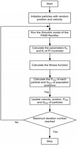
3.3 Modelling of PSO based PI controller
The PSO based PI controller is utilized to tune the PI parameters of Kp and Ki values, through which the 1-Ф PWM rectifier is controlled. This algorithm is motivated by the social performance of bird and fish schooling, which solves continuous nonlinear optimization issues. In this algorithm, the swarm is initiated with a population of random solutions and every particle in the swarm represents a different group of unknown variables that needs to be optimized. Every particle represents a point in the solution space, which adjusts its flying towards a potential area on the basis of own flying experience. When dealing with thea multidimensional issues, the following equations are used to change the velocity and location of every particle in the swarm,
$V_i^{\mathrm{k}+1}=\mathrm{V}_{\mathrm{i}}^{\mathrm{k}}+\mathrm{C}_1 \operatorname{rand}\left(\right.$ pbest $\left._{\mathrm{i}}-\mathrm{S}_{\mathrm{i}}^{\mathrm{k}}\right)+\mathrm{C}_2 \operatorname{rand}\left(\right.$ gbest $\left._{\mathrm{i}}-\mathrm{S}_{\mathrm{i}}^{\mathrm{k}}\right)$ (20)
$X_i^{k+1}=X_i^k+V_i^{k+1}$ (21)
Where the velocity of $i^{\text {th }}$ particle at $(k+1)$ iteration is denoted as $V_i^{k+1}$, the location of $i^{t h}$ particle at $(k+1)$ iteration is denoted as $X_i^{k+1}$, the inertial weight factor is denoted as w, the acceleration constants named cognitive learning rate is denoted as C1, acceleration constants named social learning rate is denoted as C2 , rand denotes the function of random in the range [0,1] , the individual best location of the particle is denoted as pbest and the global best location of the swarm particles is denoted as gbest. The flow chart of PSO based PI controller is illustrated in Figure 5.
Figure 5. Flow chart of PSO based PI controller
The inertial weight factor, $w$ is in charge of dynamically changing the particle velocity and thus balancing the local and global search. The algorithm searches globally at the start and locally at the end of the execution by using a large inertia weight at the start and decreasing it to a small value during the execution of PSO. The inertial weight factor, which is expressed as,
$w=w_{\max }-\frac{\left(w_{\max }-w_{\min }\right). \text { iter }}{\text { iter }_{\max }}$ (22)
where the initial weight is denoted as $w_{\max }$, the final weight is denoted as $w_{\text {min }}$, the current iteration time is denoted as iter and the maximum number of iteration is denoted as iter $_{\max }$. The proposed fitness function for the optimization of PI controller parameters, which is expressed as,
$F(s)=w_{\max }\left(M_p+I S E+I A E\right)+w_{\min }\left(T_R+T_S\right)$ (23)
In terms of Integral squared error (ISE) and Integral Absolute value error (IAE), the performance of the controller is estimated, which is expressed as,
$I S E=\int_0^t e^2 d t$ (24)
$I A E=\int_0^t|e| d t$ (25)
With respect to time, ISE and IAE weight the error and thus decrease the value of error, which is closer to zero. Thus, with the utilization of PSO based PI controller, the 1 — Ф PWM rectifier is controlled.
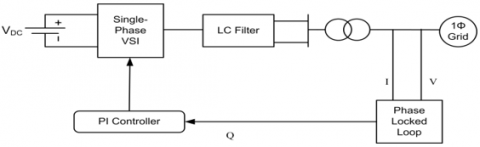
3.4 Single phase VSI and grid
To synchronize with the grid, the DC voltage attained from the 1Ф PWM rectifier is converted into AC voltage with the utilization of 1Ф VSI. The inverter employed in this scheme is full bridge 1Ф VSI that supplies power with good quality to the grid at a suitable voltage, phase angle and frequency. The schematic representation of grid connected inverter is illustrated in Fig. 6.
Figure 6. Schematic representation of grid connected inverter.
The LC filter, which is linked in the output side of 1Ф VSI eliminates the power quality issues like sag, swell etc. while synchronizing the 1Ф VSI to the utility grid, the current harmonics are reduced. The output voltage +Vs is attained by closing the switches S1 and S2 and the output voltage —Vs is attained by closing the switches S3 and S4. The phase locked loop will effectively synchronizes the grid tied inverter, since the reference voltage is locked to the utility of voltage vector phase angle. With the utilization of PI controller, the VSI is controlled by comparing Pact with Pref values and so the gating pulses for VSI are generated through which the grid synchronization and the compensation of reactive power are achieved.
To synchronize the power with the grid, energy storage device is utilized, which is named as SMES that stores large amount of electrical power and the outcome of the SMES is AC voltage. The attained AC voltage is rectified into DC voltage with the aid of 1Ф PWM rectifier, which is then fed to the grid through 1Ф VSI. With the utilization of PSO based PI controller, the PWM rectifier is controlled, which converts DC into AC voltage. With the aid of PI controller, the grid synchronization and compensation of reactive power is achieved. The proposed control scheme is simulated in the MATLAB software.
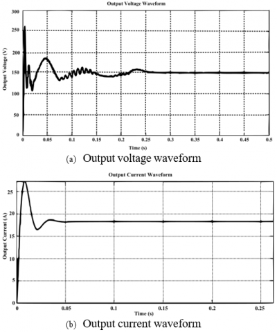
The SMES output voltage and current waveform are illustrated in Figure 7 (a) & (b). The output from the SMES is AC, in voltage waveform it is noted that, after the time 0.25s, the voltage is retained at 150V and in the current waveform it is noted that, after the time 0.05s, the current is retained at 18A.
Figure 7. SMES Output Voltage and Current waveforms
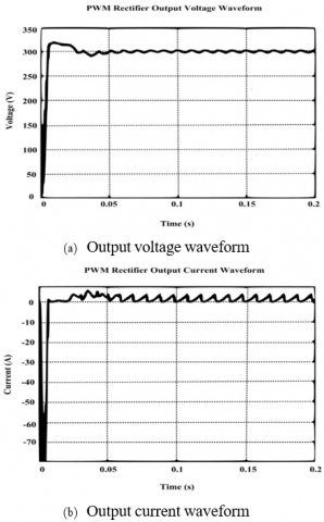
The AC output voltage generated by the SMES is fed into the 1Ф PWM rectifier which inverts the AC voltage source into DC output voltage. The voltage and current waveform of the PWM rectifier is highlighted in Figure 8(a) and (b). Hence it is keenly observed from the waveform that the generated output voltage of PWM rectifier lies between 0V and 320V.
Figure 8. PWM rectifier output voltage and current waveforms
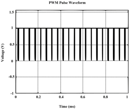
A PSO based PI controller is employed to regulate the performance of the PWM rectifier by analogizing $V_{\text {act }}$ with $V_{r e f}$. Thus, the PWM rectifier generates the appropriate gating pulses which is portrayed in Figure 9.
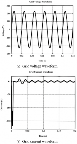
After removing the noise by using filter, the output signal generated by a single phase VSI is given to the grid. Thus the generated voltage and current waveform of the grid is highlighted in Figure 10, which shows that the grid voltage ranges from $-230 \mathrm{~V}$ to $+230 \mathrm{~V}$.
Figure 9. PWM gating pulse waveform
Figure 10. Grid voltage and current waveforms
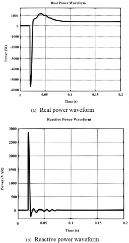
The VSI's output is regulated by the PI controller which sends appropriate sinusoidal signal to the grid by means of PWM generator. As shown in Figure 11, real power rises initially and reaches 500W while the reactive power falls down to zero.
Figure 11. Real and reactive power waveforms
Figure 12 shows that the source current THD of the suggested SMES system is very low and it is noted as 2.89 %.
Figure 12. Source current THD
The comparative analysis of source current THD is illustrated in Figure 13. From this analysis it is noted that, the source current THD for PSO based PI controller is 2.89 %, which is which is comparatively better than Fuzzy and PI controllers.
Figure 13. Comparative analysis of source current THD
In this paper, a PSO based PI controller is utilized to control the PWM rectifier through which the gating pulses are generated. The attained output from PWM rectifier is then fed to the grid through 1Ф VSI, through which the gating pulses for VSI are generated with the aid of PI controller. Also, SMES is instigated in this study that provides fast response, higher efficiency, and stores large amount of electrical power. Due to these benefits, it has the ability to eradicate the power quality issues. The output attained from the SMES is AC voltage, which is rectified into DC voltage with the aid of PWM rectifier. To synchronize with the grid, inverter converts the DC into AC voltage, through which the grid synchronization and the compensation of reactive power are achieved. Also, the source current total harmonic distortion (THD) of the proposed PSO based PI is compared with conventional methods like PI and Fuzzy controller which is less compared to the later methods.
|
PSO |
particle swarm optimization |
|
SMES |
superconducting Magnetic Energy Storage |
|
PWM |
pulse width modulation |
|
FLC |
fuzzy logic controller |
|
VSI |
voltage source inverter |
|
BESS |
battery energy storage systems |
|
HTS |
high temperature superconducting |
|
LTS |
low temperature superconductors |
|
ISE |
integral Squared Error |
|
GA |
genetic algorithm |
|
IAE |
integral Absolute value Error |
|
Q |
quantity factor |
|
PI |
Proportional-integral |
|
B |
Magnetic flux density |
|
N |
Number of turns |
|
I |
Current |
|
L |
inductance |
|
P |
power |
|
T |
time period |
|
D |
duty cycle |
|
M |
modulation index |
|
W |
integral weight factor |
|
C1 |
cognitive learning rate |
|
C2 |
social learning rate |
|
rand |
random function |
|
iter$_{\max }$ |
Maximum number of iterations |
|
Greek symbols |
|
|
Ф |
phase |
|
η |
utilization factor |
|
ω |
angular frequency |
|
Subscripts |
|
|
p |
proportional |
|
m |
maximum |
|
s |
source |
|
a |
amplitude |
|
sc |
superconducting coil |
|
act |
actual |
|
ref |
reference |
[1] SHIM, J.W., Y. CHO, K. SEOG-JOO, M. SANG WON and H. KYEON. Synergistic Control of SMES and Battery Energy Storage for Enabling Dispatchability of Renewable Energy Sources. IEEE Transactions on Applied Superconductivity. 2013, vol. 23, iss. 3, pp. 5701205-5701205. ISSN 1558-2515. DOI: 10.1109/TASC.2013.2241385
[2] MOHD., H. A., B. WU and R. A. DOUGAL. An Overview of SMES Applications in Power and Energy Systems. IEEE Transactions on Sustainable Energy. 2010, vol. 1, iss. 1, pp. 38 – 47. ISSN 1949-3029. DOI: 10.1109/TSTE.2010.2044901.
[3] BIAO, Z., Q. SONG, W. LIU and Y. SUN. A Synthetic Discrete Design Methodology of High-Frequency Isolated Bidirectional DC/DC Converter for Grid- Connected Battery Energy Storage System Using Advanced Components. IEEE Transactions on Industrial Electronics. 2014, vol. 61, iss. 10, pp. 5402 –5410. ISSN 1557-9948. DOI: 10.1109/TIE.2014.2304915.
[4] TAO, L., Y. CHEN, H. Y. GOU, X. Y. CHEN, M. G. TANG and Y. LEI. A DC Voltage Swell Compensator Based on SMES Emulator and Lead-Acid Battery. IEEE Transactions on Applied Superconductivity. 2019, vol. 29, iss. 2, pp. 1-4. ISSN 1558-2515. DOI: 10.1109/TASC.2019.2894017.
[5] ISSARACHAI, N. and S. VACHIRASRICIRIKUL. Design of Optimal SMES Controller Considering SOC and Robustness for Microgrid Stabilization. IEEE Transactions on Applied Superconductivity. 2016, vol. 26, iss. 7, pp. 1 – 5. ISSN 1558-2515. DOI: 10.1109/TASC.2016.2597261.
[6] SAICHI, Y., D. MIYAGI and M. TSUDA. A Suitable Design Method of SMES Coil for Reducing Superconducting Wire Usage Considering Maximum Magnetic Flux Density. IEEE Transactions on Applied Superconductivity. 2014, vol. 24, pp. 1 – 5. ISSN 1558- 2515. DOI: 10.1109/TASC.2013.2290279.
[7] XING, Y. Q., J. X. JIN, Y, L, WANG, B. X. DU and S. C. WANG. An Electric Vehicle Charging System Using an SMES Implanted Smart Grid. IEEE Transactions on Applied Superconductivity. 2016, vol. 26, iss. 7, pp. 1- 4. ISSN 1558-2515. DOI: 10.1109/TASC.2016.2602245.
[8] LEI, CH., H. CHEN, Y. L, G. LI, J. YANG, X. LIU, Y. XU, L. REN and Y. TANG. SMES-Battery Energy Storage System for the Stabilization of a Photovoltaic- Based Microgrid. IEEE Transactions on Applied Superconductivity. 2018, vol. 28, iss. 4, pp. 1- 7. ISSN 1558-2515. DOI: 10.1109/TASC.2018.2799544.
[9] Sewan, C. A three-phase unity-power-factor diode rectifier with active input current shaping. IEEE Transactions on Industrial Electronics. 2005, vol. 52, iss. 6, pp. 1711 – 1714. ISSN 1557-9948. DOI: 10.1109/TIE.2005.858699.
[10] RUXI, W., F. WANG, D. BOROYEVICH, R. BURGOS, R. LAI, P. NING and K. RAJASHEKARA. A High Power Density Single-Phase PWM Rectifier With Active Ripple Energy Storage. IEEE Transactions on Power Electronics, 2011, vol. 26, iss. 5, pp. 1430 – 1443. ISSN 1941-0107. DOI: 10.1109/TPEL.2010.2090670.
[11] QINGXIAO, D., L. GAO, Q. LI, T. LI and F. MENG. Harmonic Reduction Methods at DC Side of Parallel- Connected Multipulse Rectifiers: A Review. IEEE Transactions on Power Electronics. 2021, vol. 36, iss. 3, pp. 2768 – 2782. ISSN 1941-0107. DOI: 10.1109/TPEL.2020.3013407.
[12] FANGANG, M., S. YANG and W. YANG. Modeling for a Multitap Interphase Reactor in a Multipulse Diode Bridge Rectifier. IEEE Transactions on Power Electronics. 2009, vol. 24, iss. 9, pp. 2171 – 2177. ISSN 1941-0107. DOI: 10.1109/TPEL.2009.2022534.
[13] HADI, N. J., A. GOUDARZIAN, R. POURBAGHER and S. Y. DERAKHSHANDEH. PI and PWM Sliding Mode Control of POESLL Converter. IEEE Transactions on Aerospace and Electronic Systems. 2017, vol. 53, iss. 5, pp. 2167 – 2177. ISSN 1557-9603. DOI: 10.1109/TAES.2017.2684998.
[14] SAETIEO, S. and D.A. TORREY. Fuzzy logic control of a space-vector PWM current regulator for three-phase power converters. IEEE Transactions on Power Electronics. 1998, vol. 13, iss. 3, pp. 419 – 426. ISSN 1941-0107. DOI: 10.1109/63.668101.
[15] MAHAMMAD, A. H., J. A. ALI, A. MOHAMED, U. ANISA UNGKU AMIRULDDIN, N. MEI LIN TAN and MD. NASIR UDDIN. Quantum-Behaved Lightning Search Algorithm to Improve Indirect Field-Oriented Fuzzy-PI Control for IM Drive. IEEE Transactions on Industry Applications. 2018, vol. 54, iss. 4, pp. 3793 – 3805. ISSN 1939-9367. DOI: 10.1109/TIA.2018.2821644.