S. Thanikaikarasan* | R. Perumal | E Thanikaivelan | Tansir Ahamad | Saad M Alshehri
© 2023 IIETA. This article is published by IIETA and is licensed under the CC BY 4.0 license (http://creativecommons.org/licenses/by/4.0/).
OPEN ACCESS
Iron chalcogenides attracted researchers in several applications due to its prominent characteristics viz., band gap, crystalline nature and composition along with its chemical and optical properties. The main intention of the present work is to determine the modified features of iron selenide and iron diselenide thin film growth by simple electrodeposition technique. Thin films of iron selenide and iron diselenide are deposited on transparent nature conducting substrates. Structural properties reported that the deposited films found to be polycrystalline in nature. The structural parameters such as crystallite size, strain, dislocation density and stacking fault probability were determined. Microscopic images showed that deposited films have well defined morphology with nearly stoichiometry. The band gap value of the deposited films found to be around $1.21 \mathrm{eV}$.The parameters refractive index, extinction coefficient of the deposited films are estimated.
band gap, electrodeposition, ferroselite, thin films, wurtzite
Chalcogenides of iron attracted many researchers due to its extensive applications in numerous fields [1, 2] viz., photovoltaic [3], semiconductors [4], superconducting and sensing devices [5]. There is an existence of several nonstoichiometric, stoichiometric phases of iron selenide compounds such as $\mathrm{Fe}_3 \mathrm{Se}_4, \mathrm{Fe}_3 \mathrm{Se}_7, \mathrm{FeSe}_2$ and $\mathrm{FeSe}$. The stoichiometric phases of alloys $\mathrm{FeSe}_2$, FeSe are well known semimagnetic semiconductors received much attention in magnetic and spintronic applications [6]. The alloys of FeSe and $\mathrm{FeSe}_2$ found to be crystallized in hexagonal structure and orthorhombic structure. The percentage of elemental Se is in the range between 48 and 56%, determine the properties of magnetic materials such as ferromagnetic, paramagnetic and diamagnetic [6]. Thin films of FeSe and FeSe2 found to be ptype semiconductor with an energy gap value in the range between 1.23 and 1.08 eV which make them interesting for its applications in superconductors, photovoltaic and optoelectronics devices [7, 8]. Thin films of FeSe found to be crystallized in the hexagonal structure (PDF-75-0608, JCPDS ICDD 2003) with lattice constants (a = 3.61 Å; c = 5.87 Å) at lower temperature whereas FeSe2 thin films are crystallized in orthorhombic structure with lattice constants (a = 4.801 Å; b = 5.776 Å; c = 3.585 Å). Several physical and chemical techniques employed to prepare FeSe and FeSe2 thin films such as thermal evaporation, sputtering, chemical bath deposition, spray pyrolysis and so on [9-13]. The technique of electrochemical deposition has been evidenced as a powerful ability to control the crystallization of iron selenide, iron diselenide thin films and it presents a simple, economical, cost effective, less time consuming as well as adjustment of the deposition parameters with composition of electrolytic bath along with its film stoichiometry [14-16].
In the present report, thin films of FeSe and FeSe2 were deposited on transparent nature conducting ITO substrates by simple, low cost electrodeposition technique. Structural properties of the deposited films determined using X-ray diffraction. The characterization techniques viz., scanning electron microscopy, Energy dispersive X-ray analysis and UV-visible-NIR spectroscopy have been carried out to determine the surface morphology, film composition and optical properties of the deposited films.
1.1 Electrodeposition of FeSe and FeSe2 thin films
The source of chemicals $\mathrm{FeSO}_4 7 \mathrm{H}_2 \mathrm{O}, \mathrm{SeO}_2$, dilute $\mathrm{H}_2 \mathrm{SO}_4$ used were of $\mathrm{AR}$ grade reagents (E-Merck). The potentiostatic deposition of $\mathrm{FeSe}$ and $\mathrm{FeSe}_2$ was carried out using Potentiostat/Galvanostat (SP 50, Bio Logic, France) with three electrode cell arrangement consists of ITO substrate, Graphite rod and Saturated Calomel Electrode (SCE) as cathode, anode and reference electrodes, respectively. The working electrode with area of cross section $2 \times 1.5 \mathrm{~cm}^2$ were cleaned in acetone with ultrasonic bath for 15 minutes. Thereafter, they were well cleaned with running distilled water for the duration of 10 minutes. Finally the substrates were subjected to the process of drying in air for 20 minutes. The electrolytic bath consists of $0.02 \mathrm{M}$ $\mathrm{FeSO}_4, 0.002 \mathrm{M} \mathrm{SeO}_2$ for $\mathrm{FeSe}$, whereas $0.02 \mathrm{M} \mathrm{FeSO}_4, 0.02$ $\mathrm{M} \mathrm{SeO}_2$ for $\mathrm{FeSe}_2$, respectively. The films deposited at bath temperature below $50^{\circ} \mathrm{C}$, the current density is found to be lower reduces the release of ions with poor adherence nature to the substrate. If the temperature was increased above $50^{\circ} \mathrm{C}$, the rate of release of ions was found be to be higher produces films with well adherence nature to the substrate. The increase of bath temperature above $80^{\circ} \mathrm{C}$ the value of current density found to be lower resulted peel off nature of film from the substrate. As a result, the bath temperature was maintained in the range between 50 and $80^{\circ} \mathrm{C}$. The $\mathrm{pH}$ value of the electrolytic bath was initially at $4.0 \pm 0.1$, thereafter reduced to $2.5 \pm 0.1$, by the addition of an adjustable amount of dilute $\mathrm{H}_2 \mathrm{SO}_4$ to the electrolytic bath. The optimized value of $\mathrm{pH}$ was maintained in the range between 2.0 and $2.5 \pm 0.1$ to obtain films with good quality. The time of deposition was found to be in the range between 5 and 50 minutes. Also, the deposition potential was fixed in the range between -500 and $-1300 \mathrm{mV}$ versus SCE for the deposited films of FeSe and $\mathrm{FeSe}_2$.
1.2 Characterization
The method of weight difference was used to find out thickness value of the deposited films. The electrochemically grown $\mathrm{FeSe}$ and $\mathrm{FeSe}_2$ thin films were subjected to the characterization of X-ray diffraction using Phillips diffractometer at $40 \mathrm{kV}$ and $300 \mathrm{~mA}$ within the diffraction angle in between 20 and 80 degree have $\mathrm{CuK} \alpha$ target (λ = 1.5406Å). The morphological feature along with composition was analyzed using an Energy dispersive X-ray analysis set up attached with JEOL JSM 840 Scanning electron microscope. The technique of UV-Visible- NIR spectroscopy was carried out to determine the percentage of absorbance and transmittance nature of the deposited films using Shimadzu UV-Visible NIR spectrometer.
2.1 Growth kinetics
The stoichiometric growth of $\mathrm{FeSe}$ and $\mathrm{FeSe}_2$ phase takes place according to the following Eq's (1) to (4). The decomposition of $\mathrm{Fe}^{2+}$ from compound $\mathrm{FeSO}_4 7 \mathrm{H}_2 \mathrm{O}$ takes place according to Eq. (1), whereas the decomposition of $\mathrm{Se}^{2-}$ takes place according to Eq. (2)
$\begin{aligned} & \mathrm{FeSO}_4 7 \mathrm{H}_2 \mathrm{O} \rightarrow \mathrm{Fe}^{2+}+\left(\mathrm{SO}_4^{2-}\right)_3+7 \mathrm{H}_2 \mathrm{O} \\ & \mathrm{Fe}^{2+}+2 e \rightarrow \mathrm{Fe} \quad E_{\mathrm{Fe}}^0=-447 \mathrm{mV}\end{aligned}$ (1)
$E_{F e}=E_{F e}^0-\left[\frac{R T}{2 F}\right] \ln \left[\frac{a_{F e}}{a_{F e}^{2+}}\right]$
$S e^{2+}+2 e \rightarrow S e^{2-} E_{S e}^0=-930 \mathrm{mV}$ (2)
$E_{S e}=E_{S e}^0-\left[\frac{R T}{2 F}\right] \ln \left[\frac{a_{S e}}{a_{S e} z-}\right]+\left[\frac{R T}{4 F}\right] \ln \left(a_H^{+}\right)^4$
The formation of FeSe and FeSe2 takes place according to the following Eq’s (3) & (4)
$\mathrm{Fe}^{2+}+\mathrm{Se}^{2-}+4 e \rightarrow \mathrm{FeS} e$ (3)
$Fe^{2+}+2 S e^{2-}+4 e \rightarrow F e S e_2$ (4)
The growth of the deposited FeSe and FeSe2 thin film layers on ITO substrates which have been adjusted mainly by film thickness and surface morphology. The significant parameters such as current density, solution pH, bath temperature and electrolyte concentration plays an essential role to find out thickness value of the deposited films [17, 18].Thickness of the deposited films was determined from the bulk density, weight difference in which the film deposited on substrate before and after certain intervals of time. Thickness of the deposited films was calculated by using the following Eq. (5) [14]:
$t=\frac{m}{A \rho}$ (5)
Thickness of the deposited FeSe and FeSe2 thin films was found to be in the range between 1250 and 1400 nm (Table 1).
Table 1. Structural and optical parameters estimated for the deposited FeSe and FeSe2 thin films
|
Sample |
Crystallite size, P (nm) |
Rmsstrain, $<\mathrm{e}^{1 / 2}>\left(10^{-4}\right)$ (line $\mathrm{e}^{-}$${ }^2$ metre ${ }^{-4}$ ) |
Dislocation density, $(\rho)$ $\left(10^{14}\right)$ lines metre $^{-2}$ |
Lattice constant (Å) |
Atomic $(\%)$ |
Band gap,$\mathrm{E}_{\mathrm{g}}(\mathrm{eV})$ |
n |
K |
|||
|
a |
b |
c |
Fe |
Se |
|||||||
|
FeSe |
42.17 |
9.52 |
5.63 |
3.321 |
-- |
5.431 |
52.24 |
47.76 |
1.26 |
3.17 |
0.26 |
|
$\mathrm{FeSe}_2$ |
45.54 |
7.82 |
4.85 |
5.721 |
5.718 |
3.520 |
65.93 |
34.07 |
1.07 |
2.37 |
0.75 |
2.2 Structural properties
X ray diffraction pattern has been taken out to identify the crystalline nature and phases of the deposited films. XRD pattern recorded for FeSe thin films deposited on ITO substrate at optimized condition is shown in Figure 1a. It is noted that the deposited films found to exhibit hexagonal structure.The identification of peaks in the diffractogram found at 2θ values 28.49, 30.40, 42.20, 50.51, 55.35, 60.15, 7.93 and 78.26, corresponding to the lattice planes (100), (002), (102), (110), (103), (112), (202) and (203) for hexagonal FeSe, respectively [19]. The orientation of the deposited film found to be (002) along the substrate. XRD pattern recorded for FeSe2 thin films deposited on ITO substrate is shown in Figure 1b. The diffraction peaks of FeSe2 found at 2θ values 24.06, 31.07, 34.77, 36.22, 40.20, 44.42, 48.14, 49.32, 54.09 and 59.53 correspondingto the lattice planes (1 1 0), (1 0 1), (1 1 1), (1 2 0), (2 1 0), (1 2 1), (2 1 1), (2 2 0), (0 3 1) and (3 1 0), respectively [20]. The deposited films found to exhibit most prominent reflection along (120) plane along the surface. The value of lattice constants “a”, “c” for hexagonal phase FeSe and “a”, “b”, “c” for orthorhombic phase of FeSe2 are estimated using the following Eq.’s(6) & (7) [15,18]:
$\frac{1}{d^2}=\frac{4}{3}\left[\frac{h^2+h k+l^2}{a^2}\right]+\frac{l^2}{c^2}$ (6)
$\frac{1}{d^2}=\frac{h^2}{a^2}+\frac{k^2}{h^2}+\frac{l^2}{c^2}$ (7)
The value of crystallite size for the deposited FeSe and FeSe2 thin films was calculated using Debye Scherrer formula [21].
$D=\frac{0.9 \lambda}{\beta \cos \theta}$ (8)
where, $\beta$ is the Full Width at Half Maximum of the peak position in radian, $\lambda$ is the wavelength of $\mathrm{CuK}_\alpha$ target used (l= 1.540 Å), θ is Bragg diffraction angle at peak position in degree. The films deposited at lower temperature around $80^{\circ} \mathrm{C}$ found to be polycrystalline nature when compared with films obtained by other techniques viz., thermal evaporation, vaccum evaporation, sputtering, spray pyrolysis and so on.
Figure 1a,b. XRD pattern of electrodposited FeSe and FeSe2 thin films
$\mathrm{XRD}$ technique appears to be attractive to find out the value ofstrain, dislocation density and stacking fault probability of the deposited films. Strain is defined as the restricted force which can be acts along the substrate surface. The method of variance analysis given by the method Mitra has been used to estimate the value of strain present in the deposited films [22]. The rms microstrain present in the deposited films is calculated using the following Eq.(9). The number of dislocation lines present in the deposited films is termed as dislocation density [23].The value of dislocation density and stacking fault probability were determined using the following Eq.(10).
$W_{2 \theta}=\left[\frac{\lambda \theta}{\left(2 \pi^2 D \cos \theta\right)}\right]+4 \tan ^2 \theta<e^2>$ (9)
$\rho=\frac{3.46<e^2>1 / 2}{d D}$ (10)
where $\left\langle\mathrm{e}^2\right\rangle$ the microstrain, $\rho$ is the dislocation density. The stacking fault probability $(\alpha)$ is the fraction of layers undergoing stacking sequence faults in a given crystal and hence one fault is expected to be found in (1/ $\alpha)$ layers [24]. The presence of stacking faults gives rise to a shift in peak position of different reflections with respect to ideal position of a fault-free well-annealed sample and hence to evaluate the structural parameters. The values of stacking fault probability estimated for the deposited films using the following Eq. (11).
$\alpha=\left[\frac{2 \pi^2}{45 \sqrt{3}}\right]\left[\frac{\Delta(2 \theta)}{\tan \theta}\right]$ (11)
The estimated value of lattice parameters such as lattice constants, crystallite size, strain and dislocation density are given in Table 1.
2.3 Surface morphology and film composition
Morphological view along with composition for the deposited iron selenide and iron diselenide thin films was analyzed using an Energy dispersive X-ray analysis set up attached with Scanning Electron Microscopy.The SEM image with EDX spectra of FeSe thin film deposited on ITO substrate is shown in Figure $2 a$,b. It is noted that the surface is found to be smooth with coverage of spherically shaped grains. The emission lines of $\mathrm{Fe}$ and $\mathrm{Se}$ are present in the investigated energy range denoted the formation of FeSe thin films. The atomic percentage (Fe:Se) value of FeSe thin films deposited on ITO substrate is found to be 52.27:48.04. Similarly, the uniform distribution of spherically shaped grains and the composition of the deposited layers of $\mathrm{FeSe}_2$ with film composition (65.38:34.17) was analyzed and shown in Figure 3a,b. The atomic percentage of the deposited $\mathrm{FeSe}_2$ layers was found to be nearly stoichiometric nature of the deposited films. The estimated value of elemental percentage for $\mathrm{FeSe}$ and $\mathrm{FeSe}_2$ thin films are given in Table 1 (see end of article).
Figure 2a,b. SEM image and EDX spectrum of FeSe thin films
Figure 3a,b. SEM image and EDX spectrum of FeSe2 thin films
2.4 Optical properties
The knowledge of band structure with the value of energy gap in $\mathrm{eV}$ is the determination of transmittance, absorption and reflectance measurement of the deposited FeSe and $\mathrm{FeSe}_2$ films. In the present study, the percentage of optical absorbance and transmittance was recorded within the wavelength range in between 350 and $1100 \mathrm{~nm}$. The nature of transition present in the deposited films is determined by using the following Eq. (12)[16,17]
$\alpha=\frac{A\left(hv-E_g\right)^2}{hv}$ (12)
where, (hv) is the photon energy in $\mathrm{eV}, \mathrm{Eg}$ is the band gap energy in eV, $\alpha$ is the absorption coefficient in $\mathrm{cm}^{-1}$. The value of $n=1 / 2$ indicated that the direct transition of the deposited $\mathrm{FeSe}$ and $\mathrm{FeSe}_2$ thin films.
Figure 4a,b. Transmittance percentage of $\mathrm{FeSe}$ and $\mathrm{FeSe}_2$ thin films deposited on ITO substrate
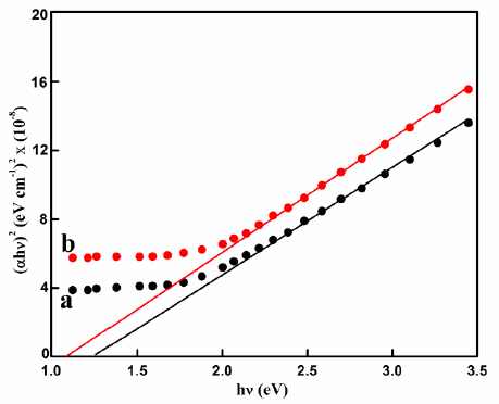
Figure 4a,b shows the percentage of transmittance for $\mathrm{FeSe}$ and $\mathrm{FeSe}_2$ thin films deposited on ITO substrate. It is noted that the percentage of transmittance is found to be maximum at 950 and $1099 \mathrm{~nm}$. The value of maximum transmittance for the deposited film is found to be is in the range between 60 and 70. The presence of maximum transmittance in the range between 960 and $1050 \mathrm{~nm}$ related to the transportation of electron from the valence band (VB) to the conduction band (CB) of the deposited films. Plot of (hv) versus $(\alpha h v)^2$ for $\mathrm{FeSe}$ and $\mathrm{FeSe}_2$ thin films deposited on ITO substrate is shown in Figure 5a,b. The linear portion of the plot to the $\mathrm{X}$-axis ( $\mathrm{h} v)$ gives band gap value of the deposited films. The deposited films found to exhibit energy gap value in between 1.04 and $1.24 \mathrm{eV}$ for $\mathrm{FeSe}$ and $\mathrm{FeSe}_2$ which must be closer to the value reported earlier $[15,18]$.
Figure 5a,b. Taucs plot for $\mathrm{FeSe}$ and $\mathrm{FeSe}_2$ thin films deposited on ITO substrate
Refractive index " $n$ " is one of the basic properties of semiconductors and it is defined as the ratio of sine angle of incidence to sine angle of refraction. The value of refractive index and extinction coefficient of the deposited films has been calculated using the following relation's.
$n=\left(\frac{1+R}{1-R}\right)-\sqrt{\frac{4 R}{1-R}}-k^2$ (13)
$k=\frac{a \lambda}{4 \pi}$ (14)
where, $\mathrm{n}$ is the refractive index, $\mathrm{k}$ is the extinction coefficient, $\lambda$ is the wavelength in nm. Variation of refractive index " $n$ " with wavelength " $\lambda$ " for FeSe and $\mathrm{FeSe}_2$ thin films is shown in Figure 6. Also the variation of extinction coefficient with wavelength for $\mathrm{FeSe}$ and $\mathrm{FeSe}_2$ thin films deposited on ITO substrate is shown in Figure 7. The decrease in value of "k" with increase in the value of " $\lambda$ " displays that the fraction of light lost due to scattering and decrease in the ratio of absorption [17]. After these wavelengths, the curves exhibited a peak due to absorption, and then these values tend to remain constant.
Figure 6a,b. Variation of refractive index (n) with wavelength $(\lambda)$ for $\mathrm{FeSe}$ and $\mathrm{FeSe}_2$ thin films deposited on ITO substrate
Figure 7a,b. Variation of extinction coefficient (k) with wavelength $(\lambda)$ for $\mathrm{FeSe}$ and $\mathrm{FeSe}_2$ thin films deposited on ITO substrate
Thin films of $\mathrm{FeSe}$ and $\mathrm{FeSe}_2$ were successfully deposited on ITO substrates by simple low temperature electrodeposition technique. Structural features showed that the deposited films found to be polycrystalline nature with hexagonal and orthorhombic structure for $\mathrm{FeSe}$ and $\mathrm{FeSe}_2$. The value of structural parameters such as crystallite size, strain, dislocation density were determined. Morphological feature showed that the films with smooth surface and well defined stoichiometry. Optical properties denoted that the band gap value was found to be 1.21 and $1.08 \mathrm{eV}$ for FeSe and $\mathrm{FeSe}_2$. The parameters such as refractive index, extinction coefficient were estimated for the deposited films.
The authors extend their sincere appreciation to the Researchers Supporting Project Number (RSP2023R6), King Saud University, Riyadh, Saudi Arabia for funding this research.
[1] Ashok U Ubale, Naina R Welekar, AmrutaV Mitkari (2014) Effect of annealing on physical properties of CBD synthesized nanocrystalline FeSe thin films Mater. Sci. Semicond. Process. 27, 280–287. https://doi.org/10.1016/j.mssp.2014.06.035
[2] Ouertani B., Ouerfelli J., Saadoun, Bessa B.,M., Ezzaouia H., Bernedè J.C., (2005) Transformation of amorphous iron oxide thin films pre deposited by spray pyrolysis into a single FeSe2 phase by selenisation Sol. Energy Mater. Sol. Cells 87,501- 511. https://doi.org/10.1016/j.solmat.2004.07.036
[3] Mitzi D.B., Yuan M., Liu W., Kellock A.J., S.J.Chey, Deline V., Schrott A.G., (2008) A High-Efficiency Solution-Deposited Thin-Film Photovoltaic Devices Adv .Mater. 765,3657–3662. https://doi.org/10.1002/adma.200800555C
[4] Tomasz Dietl (2002) Ferromagnetic Semiconductors Semicond. Sci. Technol 17, 377- 392. https://doi.org/10.1088/0268-1242/17/4/310
[5] Schöning M.J., Kloock J.P., (2007) About 20 Years of Silicon-Based Thin-Film Sensors with Chalcogenide Glass Materials for Heavy Metal Analysis: Technological Aspects of Fabrication and Miniaturization J Electroanal. Chem. 9 2029–2038. https://doi.org/10.1002/elan.200703955
[6] XWu,Z.Zhang,J.Zhang,Z.Ju,B.Li,C.Shan,D.Zhao,B.Yao,D.Shen, (2008) Growth of FeSe on general substrates by metal-organic chemical vapor deposition and the application in magnet tunnel junction devices Thin Solid Films 516, 6116–6119. https://doi.org/10.1016/j.tsf.2007.11.012
[7] X. Wu, Z.Zhang, J.Zhang, B.Li, Z.Ju, Y.Lu, B.Li, D.Shen, J. Appl. Phys.103 (2008),113501-113501-113506.
[8] A.Mars , H.Essaidi, J.Ouerfelli (2015) Optical and electrical measurement of FeSe2 thin films obtained at low temperature Mater. Sci. Semicon. Proc. 40 319–324. https://doi.org/10.1016/j.mssp.2015.06.030
[9] Ubale A., Sakhare Y., Bombatkar S., (2013) Influence of the complexing agent (Na2-EDTA) on the structural, morphological, electrical and optical properties of chemically deposited FeSe thin films, Mater. Res. Bull.48,3564–3571. https://doi.org/10.1016/j.materresbull.2013.05.064
[10] Rong Jin, Xiaoyan Pu KeZhao, Min Zhang, (2016) Structural and photovoltaic properties of FeSe2 films prepared by radio frequency magnetron sputtering Fanggong Cai, Xinsheng Yang,Hern Kim, Yong Zhao, Mater. Lett. 179 179 - 181. https://doi.org/10.1016/j.matlet.2016.05.087
[11] Ubale A., Sakhare Y., Bombatkar S., (2013) Influence of the complexing agent (Na2-EDTA) on the structural, morphological, electrical and optical properties of chemically deposited FeSe thin films, Mater. Res. Bull. 48, 3564-3571. https://doi.org/10.1016/j.materresbull.2013.05.064
[12] Chen T.K., Luo J.Y., Ke C.T., Chang H.H., Huang T.W., Yeh K.W., C.C. Chang,P.C. Hsu, C.T. Wu, M.J. Wang, M.K. Wu, (2010) Low-temperature fabrication of superconducting FeSe thin films by pulsed laser deposition Thin Solid Films 519,1540 -1545. https://doi.org/10.1016/j.tsf.2010.06.002
[13] Ubale A, Sakhare Y, J. Phys. Chem. Solids (2013) Effect of substrate temperature on optical, structural and electrical properties of FeSe thin films deposited by spray pyrolysis technique, J Phys. Chem. Solids, 74, 1464. https://doi.org/10.1016/j.jpcs.2013.05.006
[14] S.Thanikaikarasan. (2021). Role of electrolyte concentration on growth kinetics, film thickness, structural, compositional and optical properties of cadmoselite thin films through electrochemical route, J Alloys Compd 885, 160963. https://doi.org/10.1016/j.jallcom.2021.160963
[15] Thanikaikarasan S., Mahalingam T., Sundaram K., Kathalingam A., Yong Deak Kim, Taekyu Kim, (2009) Growth and characterization of electrosynthesized iron selenide thin films Vacuum, 83,1066-1072. https://doi.org/10.1016/j.vacuum.2009.01.004
[16] Jeyakumar, P., Thanikaikarasan, S. & Natarajan, B. Role of substrate in electrodeposited copper telluride thin films. J Mater Sci: Mater Electron 28, 2538–2544 (2017). https://doi.org/10.1007/s10854-016-5828-z
[17] Bharathi, B., Thanikaikarasan, S., Kollu, P. et al. Effect of substrate on electroplated copper sulphide thin films. J Mater Sci: Mater Electron 25, 5338–5344 (2014). https://doi.org/10.1007/s10854-014-2310-7
[18] Thanikaikarasan S., Mahalingam T., (2012) Influence of solution pH in electrodeposited iron diselenide thin films mpd. J Alloys Co., 511, 115-122. https://doi.org/10.1016/j.jallcom.2011.09.003
[19] Joined Council for Powder Diffracted System International Centre for Diffraction Data, Pennsylvenia, USA, 2003. File No.75-0608.
[20] Joined Council for Powder Diffracted System International Centre for Diffraction Data, Pennsylvenia, USA, 2003. File No.21-0432
[21] Cullity BD, Stock SR. Elements of X-ray diffraction. 3rd ed.London: Pearson Publishers; 2001.
[22] Mitra G B , Misra N K (1966). Background errors in X- ray diffraction parameters. Brit J Appl. Phys 17 (10) 1319-1328. https://doi.org/10.1088/0508-3443/17/10/310
[23] Williamson G K, Smallman R E (1956). Dislocation densities in some annealed and cold-worked metals from measurements on the X-ray debye-scherrer spectrum. Philos Mag. 1:34-46. https://doi.org/10.1080/14786435608238074