© 2021 IIETA. This article is published by IIETA and is licensed under the CC BY 4.0 license (http://creativecommons.org/licenses/by/4.0/).
OPEN ACCESS
For grid-connected applications, Multi-level Inverters (MLI) are mostly used, similarly to join the various RES to the grid as well as to satisfy the load demand MLIs are mostly preferred. This article presents a fuel cell-based high-gain boost converter with a single-phase five-level inverter controlled by CB-PWM techniques. A fuel cell produces a very less amount of power so to boost-up the fuel cell power to the essential power level with the help of a high-gain boost converter. The boost converter produces the required DC output power and that power is a converter to required AC power by using a single-phase five-level inverter. The MLI switches are controlled with the help of MC-PWM techniques and observe the inverter behavior in terms of THD, output ripples, and settling time. The entire work is done in MATLAB/Simulink tool as well as design a small prototype model by using the FPGA board.
Fuel Cell, High-Gain converter, MLI, MC PWM, FPGA, THD
In the current days, the usage of renewable energies is too high, the renewable energies are like solar, wind, hydro, and biogas, etc. The consumption of fossil fuels has improved as has the absorption of toxic and greenhouse gases in the atmosphere, such as SO, NO, CO, and CO. In the current days, the usage of renewable energies are is too high, the renewable energy sources are pollution-free, high availability, and less cost and maintained [1]. Renewable energies are like solar, wind, hydro, and biogas, etc.
The demand and usage of fuel cells (FC) is high in the past years. This is mainly due to their high electrical and efficiency, less noise, good dynamic response [2]. The research on FCs is increased day today and the availability of FCs is also high, among them, the PEMFC looks like a capable source to be used in houses, industries, and various distributed generation systems [3]. The key features of PEMFC are, they generate water as a residue, high efficiency as related to other FCs, and operated at minimum temperatures [4].
The fuel cell and PV cells generate low output power, to generating a high output power the fuel cells and PV cells are arranged in series connection. In this case, the shadow effect will come so it's not a good solution for generating high output power [5]. Then connect the boost converter to the PV cells to generate a huge voltage. The conventional boost converter produces high voltage with more duty cycle but in the experimental, the standard boost converter unable to generate a high voltage at the output side due to reverse recovery issue. Because of this problem, the overall efficiency of the system is decreased, and electromagnetic interference (EMI) problem also occurs [6]. For improving high-voltage and efficiency so many step-up converter topologies are examined so far [7]. Few converters, fly back and forward converters can regulate the transformer turns ratio to get high-voltage [8].
The modified converter has two diodes and two capacitors on the secondary side of the CI. Those two capacitors are discharged in series and charged in parallel through the CI, still, high-voltage spikes and power loss are present across the switch because of the leakage inductor of the CI [9]. Thus, LI energy is reused and the voltage level of the switch is clamped by using a clamping circuit. Finally, one more diode is added on the front side of the converter it protects the system in case of reverse direction of current flow in the circuit. By using a PI controller to control the switching pulse of the high-gain boost converter [10].
After the boost converter, a single-phase five-level inverter was placed, it converts the required DC to AC power and delivers to the load. For converting DC to AC power number of inverter topologies are available [11-12]. MLIs have some remarkable futures such as lower values of harmonics distortion, good quality of the power, lesser filtering requirements, and reduces switching stress as compared to the conventional inverter topologies [13-14].
The presented inverter topology contains only five switches out of five switches four switches are arranged like an H-Bridge and the remaining one switch is works as an auxiliary switch. The switches in the inverter are controller by using three different carrier-based PWM techniques.
The entire work is done in MATLAB/Simulink tool as well as design a small prototype model by using the Spartan6 lx9 TQ144 FPGA board.
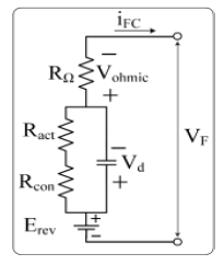
The corresponding circuit diagram of the fuel cell is represented below. This model is implemented by a set of the following equations. The single-cell output voltage is represented in equation (1) and Figure 1 signifies the equivalent circuit of FC.
$V_{F}=E_{r e v}-V_{a c t}-V_{o h m i c}-V_{c o m}$ (1)
In the above equation, Vrev is the thermodynamic potential of the individual cell, Vact is the voltage loss due to activation cathode and anode. Vohm is ohmic voltage drop, Vcom is the voltage glass due to the concentration reduction of the reactants. If ‘N’ cells are connected, then the output can be represented by
Figure 1. Equivalent circuit of FC
$V_{T}=N^{*} V_{F}$ (2)
$E_{\text {rev }}, V_{\text {act }}, V_{\text {ohmic }}, V_{\text {com }}$ are given by
$E_{r e v}=E_{o}+0.5 * R T / F *\left\lceil\operatorname{In}\left(P_{H}\right)+0.5 * \operatorname{In}\left(P_{O}\right)\right\rceil$
$\left[\begin{array}{lll} & 2 & 2\end{array}\right]$ (3)
Whereas Co2 is the concentration of oxygen and given by
$V_{a c t}=\xi 1+T\left[\xi_{L}+\xi_{3} * \operatorname{In}\left(C_{O}\right)+\xi_{2} * \operatorname{In}\left(i_{F C}\right)\right]$ (4)
$C_{O_{2}}=\frac{P_{O_{2}}}{5.08 * 10^{6} * e^{-498 / T}}$ (5)
$V_{c o m}=-B * \operatorname{In}\left(\frac{J_{\max }-J}{J_{\max }}\right)$ (6)
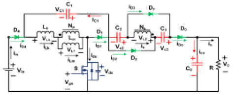
The modified High-voltage DC-DC converter has 48V DC input voltage (Vin), one coupled inductor (CI), the CI has Ns and Np, one main switch (S), output capacitor (C0), output diode (D0), clamp capacitor (C1), clamp diode (D1), two diodes (D2 and D3) and two capacitors (C2 and C3). The CI has leakage inductor (LI) Lk, magnetizing inductor (MI) Lm, and an ideal transformer. Figure 2 signifies the circuit diagram of the High-Voltage DC-DC converter. The energy in the LI of the CI is reused to C1, and the switch voltage is also clamped. The voltage stress across the switch is decreased randomly because the switch has less resistance. The innovative voltage-clamp topology was primarily projected in [15]to recover the energy in the LI. The modified converterhas an association with the CI and switched-capacitor methods.The concept of the switch capacitor method has beensuggested in [16]. So, when the switch is in an active statethose two capacitors are discharged in series similarly whenthe switch is in an inactive state those two capacitors arecharged in parallel through the CI. By tuning the CI turns ratio,the voltage around the capacitors can be controlled then high-voltage can be attained. Therefore, the modified converter hasless conduction loss and reduces the reverse-recovery problemof the diodes.
Figure 2. Circuit diagram of the modified Converter
The single-phase five-level inverter contains five IGBT switches out of five switches, four switches (S1, S2, S3, and S4) are acting like an H-bride circuit and the remaining one switch (S5) contains four diodes it acts as an auxiliary switch. The switches S3 and S4 are operated at the fundamental frequency (50Hz) and the remaining switches S1, S2, and S5 are operated at switching frequency (2k Hz). The single-phase inverter is operated in five different modes and it produces five different level output voltages. In mode-I, S4 and S5 are in ON state, rest of the switches are in OFF state, in mode-II, S1 and S4 are in ON state, rest of the switches are in OFF state, in mode-III, S3 and S5 are in ON state, rest of the switches are in OFF state, in mode-IV, S2 and S3 are in ON state, rest of the switches are in OFF state, in mode-V, S1 and S2 are in ON state, either S3 and S4 are in ON state, rest of the switches are in OFF state. Figure 3 signify the block diagram of the single- phase five-level inverter.
As the name suggested its field-programmable means the programming of the device is can be done at the customer end. It drastically reduces the device turnaround time so that’s why it is very popular. And also, many cases it is reprogrammable so easily change the design, if there is an error can very easily correct it or any modification and any up-gradation of the design those things can be carried out easily. The FPGA is started with logic gates in (1950-60) then there were regular structures for two-level logic gates in (1960-70), the two-level logic means AND level and OR level this is the PLAs type of structures. Then from they are evolving to more complex programmable devices which are known as PLDs and complex PLDs (CPLDs) that was in (1970-80). Then can the programmable gate arrays, it means can get the array of gates of similar types then connect them in some faction to get the overall functional implement. In FPGA densities high enough to permit an entirely new class of application, e. g., photo typing, emulation, acceleration. An FPGA contains mainly three parts those are logical blocks, Interconnects, I/O blocks.
Figure 3. Block diagram of the single-phase five-level inverter
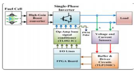
A prototype model of a single-phase five-level inverter was designed with the help of an FPGA board. A developed Spartan6 lx9 TQ144 FPGA board was used to implement the hardware setup to validate the simulation results of the proposed system. In the hardware implementation Spartan6 lx9 TQ144 FPGA, FGA15N120 (IGBT), BYQ28E (Diode), TLP250IC (Driver IC), CD4081 (AND gate IC), and TL082 IC (OPAMP IC) is used. The prototype contains mainly one FPGA board, five IGBT switches, four diodes, five driver circuits, one AND gate IC, and one Op-amp IC.
Here, the Op-amp based signal conditioner (TL082 IC) is getting the voltage and current signals from the sensors and pass that to the ADC in the FPGA board. In that FPGA board contains logic gates by using those logic gates control algorithm is implements. The buffer and driver (TLP250IC) circuit also present in the FPGA board, the driver circuit gives proper switching pulse to the inverter switches. The inverter switches are controlled by three different carrier based PWM techniques those are PD, POD, and APOD. In our prototype model, these three techniques are implemented and operated by using external switches to change the PWM techniques (PD, POD, and APOD) in the FPGA board. Figure 4 represents the hardware setup for the proposed system.
Figure 4. Hardware setup for the proposed system
In the hardware, note down and observe the corresponding load voltages and currents of the proposed system. The load voltage and current values are taken at different modulation index values, here the modulation index values are taken as 0.99, 0.9, 0.7, and 0.5. Observed the load voltage and current values of the proposed system with three different CB-PWM techniques (PD, POD, and APOD) at various modulation index values.
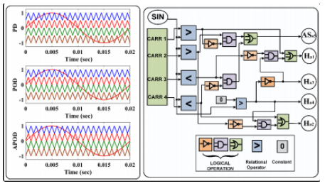
The switches in the single-phase five-level inverter were controlled by three different carrier-based PWM techniques those are PD-PWM, POD-PWM, and APOD PWM. Figure 5 represents the carrier-based PWM techniques with logic. In PD-PWM four carriers and one reference sine signal are considered, the four carriers are compared with the sine signal to produce corresponding pulse single to inverter switches. In PD-PWM all four carriers are arranged in equal phase shift and equal magnitude. In POD-PWM four carriers and one reference sine signal are considered, the four carriers are compared with the sine signal to produce corresponding pulse single to inverter switches. In POD-PWM two carriers are maintaining 90 degrees phase shift with the other two carriers and all carriers are maintain equal magnitude. In APOD-PWM four carriers and one reference sine signal are considered, the four carriers are compared with the sine signal to produce corresponding pulse single to inverter switches. In APOD PWM each carrier is maintained 90 degrees phase shift with other carrier and all carriers are maintain equal magnitude.
Figure 5. Carrier-based PWM techniques with logic
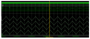
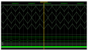
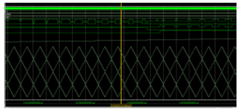
In this section, the hardware results of the single-phase five level inverter have discoursed in detail. For taking the hardware results in an open-loop system the modulation indexes are taken from 0.99, 0.9. 0.7, and 0.5, so totally four different modulation index cases are considered for analyzing the simulation results as well as hardware results. The switches in the single-phase five-level inverter were controlled by three different carrier-based PWM techniques those are PD-PWM, POD-PWM, and APOD-PWM. Figure 6 represents the simulated waveform of the PD-PWM technique using VHDL coding. Figures 7 and 8 represents the simulated waveform of POD-PWM and APOD-PWM technique using VHDL coding. The inverter switching sequence is shown in Figure 9 and 10. It is observed that the switching patterns of hardware are exactly matched with simulation.
Figure 6. The simulated waveform of PD-PWM technique using VHDL coding
Figure 7. The simulated waveform of the POD-PWM technique using VHDL coding
Figure 8. The simulated waveform of the APOD-PWM technique using VHDL coding
Case I: At MI = 0.99
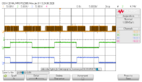
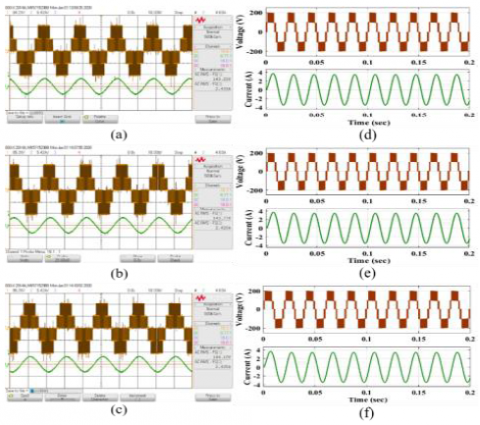
At MI=0.99, the inverter hardware output voltage (brown colored) and current (green colored) waveforms and their corresponding RMS values by using the PD-PWM technique is represented in Figure 11 (a). Figure 11 (b) depicts the inverter hardware output voltage and current waveforms with their RMS values by using the POD-PWM technique. Figure 11 (c) depicts inverter hardware output the voltage and current waveforms with their RMS values by using the APOD-PWM technique. Similarly, at MI=0.99, the inverter simulation output voltage (brown color) and current (green colored) waveforms by using the PD-PWM technique is shown in Figure 11 (d). Figure 11 (e) depicts the inverter simulation output voltage and current waveforms by using the POD- PWM technique. Figure 11 (f) depicts the inverter simulation output voltage and current waveforms by using APOD-PWM.
Case II: At MI=0.9
At MI=0.9, the inverter hardware output voltage (brown colored) and current (green colored) waveforms and their corresponding RMS values by using the PD-PWM technique are shown in Figure 12 (a). Figure 12 (b) depicts the inverter hardware output voltage and current waveforms with their RMS values by using POD-PWM technique. Figure 12 (c) depicts inverter hardware output the voltage and current waveforms with their RMS values by using the APOD-PWM technique. Similarly, at MI=0.99, the inverter simulation output voltage (brown colored) and current (green colored) waveforms by using the PD-PWM technique is shown in Figure. 12 (d) Figure 12 (e) depicts the inverter simulation output voltage and current waveforms by using POD-PWM technique. Figure 12 (f) depicts the inverter simulation output voltage and current waveforms by using APOD-PWM
Figure 9. Switching pattern T5, T3, & T4
Figure 10. Switching pattern T5, T1 & T2
Case III: At MI=0.7
At MI=0.7, the inverter hardware output voltage (brown colored) and current (green colored) waveforms and their corresponding RMS values by using the PD-PWM technique is shown in Figure 13 (a). Figure 13 (b) depicts the inverter hardware output voltage and current waveforms with their RMS values by using the POD-PWM technique. Figure 13 (c) depicts inverter hardware output the voltage and current waveforms with their RMS values by using the APOD-PWM technique. Similarly, at MI=0.99, the inverter simulation output voltage (brown colored) and current (green colored) waveforms by using the PD-PWM technique is shown in Figure 13 (d). Figure 13 (e) depicts the inverter simulation output voltage and current waveforms by using the POD PWM technique. Figure 13 (f) depicts the inverter simulation output voltage and current waveforms by using APOD-PWM.
Case IV: At MI=0.5
At MI=0.5, the inverter hardware output voltage (brown colored) and current (green colored) waveforms and their corresponding RMS values by using the PD-PWM technique is represented in Figure 14 (a). Figure 14 (b) depicts the inverter hardware output voltage and current waveforms with their RMS values by using the POD-PWM technique. Figure 14 (c) depicts inverter hardware output the voltage and current waveforms with their RMS values by using the APOD-PWM technique. Similarly, at MI=0.99, the inverter simulation output voltage (brown colored) and current (green colored) waveforms by using the PD-PWM technique is shown in Figure 14 (d). Figure 14 (e) depicts the inverter simulation output voltage and current waveforms by using the POD- PWM technique. Figure 14 (f) depicts the inverter simulation output voltage and current waveforms by using APOD-PWM.
Figure 11. Hardware and simulation Output waveforms of single-phase five-level inverter at an MI of 0.99
Figure 12. Hardware and simulation Output waveforms of single-phase five-level inverter at an MI of 0.9
The RMS values of single-phase inverter hardware output voltages and currents by using PD-PWM, POD-PWM and APOD-PWM techniques are 143.22V and 2.433A, 143.77V and 2.420A and, 144.10V and 2.425A respectively, at an MI of 0.99. The RMS values of single-phase inverter hardware output voltages and currents by using PD-PWM, POD-PWM and APOD-PWM techniques are 130.51V and 2.188A, 128.86V and 2.160A and, 128.1V and 2.170A respectively, at an MI of 0.9. The RMS values of single-phase inverter hardware output voltages and currents by using PD-PWM, POD-PWM, and APOD-PWM techniques are 98.15V and 1.652A, 98.12V, and 1.653A and, 98.28V and 1.652A respectively, at an MI of 0.7. The RMS values of single-phase inverter hardware output voltages and currents by using PD- PWM, POD-PWM, and APOD-PWM techniques are 72.69V and 1.206A, 72.53V and 1.203A and, 72.92V and 1.22A respectively, at an MI of 0.5. Table 1 represents the RMS values of single-phase five-level inverter hardware output voltages and currents by using PD-PWM, POD-PWM, and APOD-PWM techniques.
Figure 13. Hardware and simulation Output waveforms of single-phase five-level inverter at an MI of 0.7
Figure 14. Hardware and simulation Output waveforms of single-phase five-level inverter at an MI of 0.5
Table 1. Voltage and current values of single-phase five-level inverter with different CB-PWM techniques (Hardware) CB- PWM techniques
|
CB- PWM techniques |
|||||||
|
S. No |
Modulation Index (MI) |
PD-PWM |
POD-PWM |
APOD-PWM |
|||
|
Voltage in RMS |
Current in RMS |
Voltage in RMS |
Current in RMS |
Voltage in RMS |
Current in RMS |
||
|
1 |
0.99 |
143.22 |
2.433 |
143.77 |
2.420 |
144.10 |
2.425 |
|
2 |
0.9 |
130.51 |
2.188 |
128.86 |
2.160 |
128.1 |
2.170 |
|
3 |
0.7 |
98.15 |
1.652 |
98.12 |
1.653 |
98.28 |
1.655 |
|
4 |
0.5 |
72.69 |
1.206 |
72.53 |
1.203 |
72.92 |
1.22 |
Table 2. Voltage and current values of single-phase five-level inverter with different CB-PWM techniques (Simulation) CB-PWM techniques (New)
|
CB-PWM techniques (New) |
|||||||
|
S. No |
Modulation Index (MI) |
PD-PWM |
POD-PWM |
APOD-PWM |
|||
|
Voltage in RMS |
Current in RMS |
Voltage in RMS |
Current in RMS |
Voltage in RMS |
Current in RMS |
||
|
1 |
0.99 |
145.3 |
2.498 |
145.3 |
2.501 |
145.2 |
2.498 |
|
2 |
0.9 |
134.3 |
2.273 |
134.3 |
2.273 |
134.3 |
2.273 |
|
3 |
0.7 |
107.4 |
1.768 |
107.2 |
1.765 |
107.4 |
1.768 |
|
4 |
0.5 |
79.53 |
1.255 |
79.48 |
1.256 |
79.48 |
1.256 |
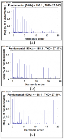
Figure 15. Inverter voltage THD at an MI of 0.99
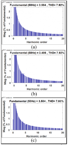
Figure 16. Inverter current THD at an MI of 0.99
The RMS values of single-phase inverter simulation output voltages and currents by using PD-PWM, POD-PWM and APOD-PWM techniques are 145.3V and 2.498A, 145.3V, and 2.501A and, 144.2V and 2.498A respectively, at an MI of 0.99. The RMS values of single-phase inverter simulation output voltages and currents by using PD-PWM, POD-PWM and APOD-PWM techniques are 134.3V and 2.273A, 134.3V, and 2.273A and, 134.3V and 2.273A respectively, at an MI of 0.9. The RMS values of single-phase inverter simulation output voltages and currents by using PD-PWM, POD-PWM and APOD-PWM techniques are 107.4V and 1.768A, 107.2V, and 1.765A and, 107.4V and 1.768A respectively, at an MI of 0.7. The RMS values of single-phase inverter simulation output voltages and currents by using PD-PWM, POD-PWM, and APOD-PWM techniques are 79.53V and 1.255A, 79.48V and 1.256A and, 79.48V and 1.256A respectively, at an MI of 0.5. Table 2 represents the RMS values of single-phase five-level inverter simulation output voltages and currents by using PD- PWM, POD-PWM, and APOD-PWM techniques.
The %THD of the inverter is also analyzed in terms of voltage and current of CB-PWM techniques with modulation index at 0.99, 0.9, 0.7, and 0.5.
Figure 15 represents the voltage %THDs values of the inverter by using CB-PWM techniques are 27.06%, 27.17%, and 27.41% respectively, at an MI of 0.99. Figure 16 represents the current %THDs values of the inverter by using CB-PWM techniques are 7.92%, 7.92%, and 7.93% respectively, at an MI of 0.99.
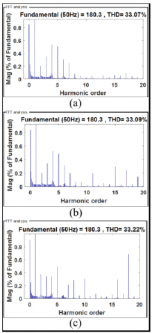
Figure 17. Inverter voltage THD at an MI of 0.9
Figure 18. Inverter current THD at an MI of 0.9
Figure 17 represents the voltage %THDs values of the inverter by using CB-PWM techniques are 33.07%, 33.09%, and 33.22% respectively, at an MI of 0.9. Figure 18 represents the current %THDs values of the inverter by using CB-PWM techniques are 7.93%, 7.95%, and 7.95% respectively, at an MI of 0.9
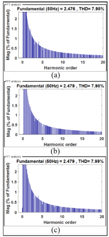
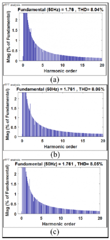
Figure 19 represents the voltage %THDs values of the inverter by using CB-PWM techniques are 41.61%, 41.71%, and 41.74% respectively, at an MI of 0.7. Figure 20 represents the current %THDs values of the inverter by using CB-PWM techniques are 7.98%, 7.98%, and 7.99% respectively, at an MI of 0.7. Figure 21 represents the voltage %THDs values of the inverter by using CB-PWM techniques are 52.32%, 52.32%, and 52.55% respectively, at an MI of 0.5. Figure 22 represents the current %THDs values of the inverter by using CB-PWM techniques are 8.04%, 8.05%, and 8.05% respectively, at an MI of 0.5. Tables 3 and 4 represents the voltage and current %THD values of single-phase inverter.
Figure 19. Inverter voltage THD at an MI of 0.7
Figure 20. Inverter current THD at an MI of 0.7
Table 3. Voltage %THD values of single-phase five-level inverter
|
S. No |
MI |
% THD of Current |
||
|
PD |
POD |
APOD |
||
|
1 |
0.99 |
27.06 |
27.17 |
27.41 |
|
2 |
0.9 |
33.07 |
33.09 |
33.22 |
|
3 |
0.7 |
41.61 |
41.71 |
41.74 |
|
4 |
0.5 |
53.32 |
52.32 |
52.55 |
Table 4. Current %THD values of single-phase five-level inverter
|
S. No |
MI |
% THD of Current |
||
|
PD |
POD |
APOD |
||
|
1 |
0.99 |
7.92 |
7.92 |
7.93 |
|
2 |
0.9 |
7.93 |
7.95 |
7.95 |
|
3 |
0.7 |
7.98 |
7.98 |
7.99 |
|
4 |
0.5 |
8.04 |
8.05 |
8.05 |
Figure 21. Inverter voltage THD at an MI of 0.5
Figure 22. Inverter current THD at an MI of 0.5
A fuel cell-based high-gain boost converter with a single-phase five-level inverter was presented in this article. Here, a fuel cell is taken as an input to the high-gain boost converter, the boost converter gives the required DC power to the inverter. The inverter switches are getting gate pulse from the MC-PWM techniques (PD, POD, and APOD). In this to observe the inverter performance in terms of THD and similarly, the inverter outputs voltage and current produce fewer ripples and less settling time. The entire work is done in MATLAB/Simulink tool as well as designed a small prototype model by using the FPGA board.
|
APOD |
Alternative Phase opposition Disposition B Constant (V) |
|
CB-PWM |
Carrier-Based Pulse Width Modulation CI Coupled Inductor |
|
Co2 |
Oxygen in the catalytic |
|
Erev |
Thermodynamic potential of the cell (V) FC Fuel Cell |
|
FPGA |
Field Programmed Array |
|
J |
Cell current density (A cm_2) |
|
Jmax |
Maximum current density (A cm_2) Jn No-load current density |
|
(A cm_2) |
LI Leakage Inductor |
|
MI |
Modulation Index |
|
MLI |
Multi-level Inverter |
|
N |
Number of cells |
|
PD |
Phase Disposition |
|
PEMFC |
Proton-exchange membrane fuel cell PO2 Partial pressure of oxygen (atm) |
|
POD |
Phase opposition Disposition RES Renewable energy source |
|
T |
Absolute cell temperature (K) THD Total Harmonic Distortion |
|
Vact |
Voltage drop due to the activation of the anode and cathode (V) |
|
Vcom |
Voltage drop of concentration of the reactants gases (V) |
|
VF |
Cell output voltage (V) |
|
Vohmic |
Ohmic voltage drop (V) |
|
VT |
Total voltage |
[1] Correa, J.M., Farret, F.A., Popov, V.A., Simoes, M.G. (2005). Sensitivity analysis of the modeling parameters used in simulation of proton exchange membrane fuel cells. IEEE Transactions on energy conversion, 20(1): 211-218. https://doi.org/10.1109/TEC.2004.842382
[2] Correa, J.M., Farret, F.A., Canha, L.N. (2001). An analysis of the dynamic performance of proton exchange membrane fuel cells using an electrochemical model. In IECON'01. 27th Annual Conference of the IEEE Industrial Electronics Society, 1(37243): 141-146. https://doi.org/10.1109/IECON.2001.976469
[3] Mann, R.F., Amphlett, J.C., Hooper, M.A., Jensen, H.M., Peppley, B.A., Roberge, P.R. (2000). Development and application of a generalised steady-state electrochemical model for a PEM fuel cell. Journal of power sources, 86(1-2): 173-180. https://doi.org/10.1016/S0378-7753(99)00484-X
[4] Baschuk, J.J., Li, X. (2000). Modelling of polymer electrolyte membrane fuel cells with variable degrees of water flooding. Journal of power sources, 86(1-2): 181-196. https://doi.org/10.1016/S0378-7753(99)00426-7
[5] Wai, R.J., Duan, R.Y. (2005). High-efficiency DC/DC converter with high voltage gain. IEE Proceedings-Electric Power Applications, 152(4): 793-802. https://doi.org/10.1109/IECON.2004.1433412
[6] Tseng, K.C., Liang, T.J. (2004). Novel high-efficiency step-up converter. IEE Proceedings-Electric Power Applications, 151(2): 182-190. https://doi.org/10.1049/ip-epa:20040022
[7] Changchien, S.K., Liang, T.J., Chen, J.F., Yang, L.S. (2010). Step-up DC-DC converter by coupled inductor and voltage-lift technique. IET power electronics, 3(3): 369-378. https://doi.org/10.1049/iet-pel.2009.0089
[8] Axelrod, B., Berkovich, Y., Ioinovici, A. (2008). Switched-capacitor/switched-inductor structures for getting transformerless hybrid DC–DC PWM converters. IEEE Transactions on Circuits and Systems I: Regular Papers, 55(2): 687-696. https://doi.org/10.1109/TCSI.2008.916403
[9] Rahim, N. A., Selvaraj, J. (2009). Multistring five-level inverter with novel PWM control scheme for PV application. IEEE transactions on industrial electronics, 57(6): 2111-2123. https://doi.org/10.1109/TIE.2009.2034683
[10] Dasari, M.S., Mani, V. (2020). Simulation and analysis of three-phase parallel inverter using multicarrier PWM control schemes. SN Applied Sciences, 2(5): 1-10. https://doi.org/10.1007/s42452-020-2772-6
[11] Hintz, A., Prasanna, U.R., Rajashekara, K. (2016). Comparative study of the three-phase grid-connected inverter sharing unbalanced three-phase and/or single-phase systems. IEEE Transactions on Industry Applications, 52(6): 5156-5164. https://doi.org/10.1109/ECCE.2015.7310569
[12] Pires, V.F., Foito, D., Cordeiro, A. (2019). PV power conditioning system using a three-phase multilevel pulse width modulation inverter employing cascaded Scott transformers. IET Power Electronics, 12(1): 102-111. https://doi.org/10.1049/iet-pel.2018.5586
[13] Kumar Kalilasam, R., Mani, V. (2018). FPGA based quasi z-source cascaded multilevel inverter using multicarrier PWM techniques. Journal of Vibroengineering, 20(3): 1544-1553. https://doi.org/10.21595/jve.2017.18180
[14] Jayabalan, M., Jeevarathinam, B., Sandirasegarane, T. (2017). Reduced switch count pulse width modulated multilevel inverter. IET Power Electronics, 10(1): 10-17. https://doi.org/10.1049/iet-pel.2015.0720