Erik Martínez-Vera*![]() | Pedro Bañuelos-Sánchez
| Pedro Bañuelos-Sánchez![]() | Alfredo Rosado-Muñoz
| Alfredo Rosado-Muñoz![]()
© 2024 The authors. This article is published by IIETA and is licensed under the CC BY 4.0 license (http://creativecommons.org/licenses/by/4.0/).
OPEN ACCESS
Electric vehicles (EVs) are an alternative to fossil-fuel-powered vehicles. However, high prices make them inaccessible for mass market adoption. Power electronics are a key enabler of vehicle electrification. In this work, the design of a bidirectional converter control is performed for application in EVs. A bidirectional topology with step-up and step-down capabilities is designed. Proportional-Integral-Derivative (PID) is the elementary control method and the most popular in power converters due to its ease of implementation, scalability, low hardware-resources requirement, and high switching frequency capability. New Wide Band Gap semiconductor devices allow to increase switching frequency to reduce the size of the converter. Design validation through in-the-loop methodologies verify that algorithms are ready for chip deployment identifying design flaws early through its development. In this work, the control algorithm for a bidirectional DC-DC converter employing WBG devices at EV power ratings is implemented. Step-up and step-down modes of operation in a cascaded bidirectional topology are analyzed with input voltage of 400 VDC, 13kW power rating, 500 kHz switching frequency and FPGA-in-the-loop (FIL) validation. FIL methodology proved a cost-effective approach to verify that control algorithms are capable for hardware deployment without the need for expensive hardware setups.
bidirectional DC-DC converter, electric vehicles, FPGA-in-the-loop, converter control
Transportation systems are powered almost entirely by petroleum-derived fuels [1]. Exhaust emissions from fossil-fuel-powered vehicles are a source of Green House Gasses (GHG) and toxic pollutants which contribute to climate change and low air quality in urban areas [2, 3]. Electric vehicles present an alternative to fossil-fuel-powered vehicles, but their high prices prevent them from mass market adoption [4]. Therefore, the development of low-cost, efficient power electronics is necessary to achieve full Transportation Electrification. In electric vehicles, the battery provides charge to the propulsion motor and low power loads. During braking, kinetic energy from the motor can be used to recharge the battery. Then, bidirectional DC-DC converters are required to handle the flow of power in both directions. Different approaches have been proposed to improve efficiency and power density while decreasing the cost of converters: circuit topology design, semiconductor material and control methodology. The circuit topology is designed based on the intended application within the EV. Isolated topologies are required for charging while propulsion and DC-link work without it [5]. Multilevel topologies reduce the current ripple and voltage stress which allows using low power components [6]. Low parts count is a desired feature to reduce cost and increase power density [7]. Hybrid Energy Storage systems include additional sources of energy asides from the battery such as Ultra-Capacitors (UC) or Photovoltaic Panels (PV), each one requiring a dedicated power converter. Then, multi-input/output converters are designed to avoid including additional converters [8, 9]. All previous designs considered Silicon (Si) power switches for experimental validation. Si devices are a mature technology that has reached development limits due to intrinsic material properties. New power switches developed from Wide Band Gap (WBG) materials present higher switching frequency and power capabilities [10]. Silicon Carbide (SiC) and Gallium Nitride (GaN) are examples of WBG materials. Higher switching frequencies allowed for reduce the size of components [6, 11-13].
Control methods for power converters aim to improve efficiency by reducing large transients and voltage overshoots. Different methods have been proposed for converter control: Proportional-Integral-Derivative (PID), Model Predictive Control (MPC), and Sliding Mode Control (SMC), among others [14]. For instance, in a multilevel converter [9], three PI controllers regulate the duty cycles of ten power switches. Control design was based on bandwidth and stability margins. An adaptive voltage scaling (AVS) control was implemented in [15] for a buck converter. Coarse and fine scaling were used to increase the speed of the converter.
FPGAs have become more popular than traditional digital signal processing units due to their greater flexibility and parallel processing capabilities for various applications [16-18]. Validation of the control design can be accomplished through FPGA-in-the-loop (FIL) methods. Then, the FIL approach allows to accelerate the design procedure by ensuring proper deployment on an actual chip [19]. PID and Generalized Proportional Integral (GPI) controllers were FPGA-implemented for a basic buck topology in the study [20]. GPI showed faster settling times compared to PID and, without voltage overshoot. Reference [21] proposed a fast MPC for a buck converter. The algorithm obtained faster settling times without voltage overshoot when compared to PID control. Real-time validation of the control method was implemented with an FPGA. However, the proposed buck converter uses an elementary topology with a low-voltage low-power design. Dual-Active-Bridge (DAB) is a popular topology due to its capability for isolation, bidirectional power flow and efficiency. It consists of two H-bridges linked by a transformer. Power flow is generated by a Phase Shift (PS) between the input and output bridges. Proportional Integral (PI) was used to estimate the required number of PS between the bridges and, implemented for 5 DAB converters with a single FPGA [22]. A bidirectional converter control was designed for an EV application in the [23]. The converter interfaced between the high-voltage battery and the motor. Ziegler-Nichols rules for PI tunning were applied. The control design was validated with FIL methodology.
From the approaches reviewed above and from a comprehensive review about bidirectional DC-DC converters with specific applications in EVs [24], DC-DC converters have been implemented either at low power and high switching frequency or conversely. Also, buck operating mode is the most reviewed at higher switching frequency without considering bidirectionality and boost capabilities [25]. Therefore, in this work, a bidirectional DC-DC converter with PID control and FIL validation for applications in electric vehicles is proposed. PID is the most popular control method due to its ease of implementation, scalability, and low hardware requirements. Then, it has become the benchmark methodology for performance comparison. FIL validation will ensure that the control design is hardware-deployment-ready. Converter design will consider high switching frequencies from WBG devices. Then, the contribution of this work is to provide a benchmark control design of a bidirectional DC-DC converter for applications in electric vehicles that includes WBG devices at switching frequencies and power ratings higher than those implemented with traditional Si devices, while operating in buck and boost modes. Additionally, FIL validation in a low-resource FPGA ensures the algorithm provides a cost-effective solution to advance vehicle electrification. The rest of the paper is divided as follows: Section 2 presents the design of the bidirectional converter, Section 3 details the control design, Section 4 shows the FIL implementation and section 5 concludes the research.
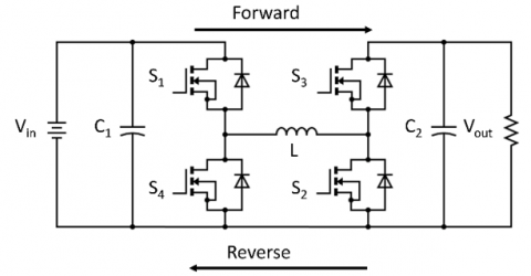
Figure 1 shows the selected bidirectional converter circuit topology for this work. This topology was selected because it has voltage overlapping with half-bridges to reduce voltage stress in components, it has interleaving capabilities and, full bidirectional power flow in buck-boost mode can be achieved [26]. Also, it has been proposed to interface between the battery and the motor in EV powertrains [27].
Figure 1. Bidirectional Converter circuit topology with two half-bridges and inductor in the middle [14, 26, 27]
For the given topology, four modes of operation can be obtained according to the status of the power switches. Table 1 shows the operating mode and the switch status for each mode. Buck and boost operation in forward and reverse modes can be achieved. In forward mode, power flows from the battery to the motor. In reverse mode, regenerative braking provides power from the motor to the battery. Next, the converter design in buck and boost modes is presented. Only forward operation is considered since the reverse operation is symmetrical and the same analysis applies.
Table 1. Operating modes of bidirectional converter
|
Mode |
Direction |
S1 |
S2 |
S3 |
S4 |
|
Buck |
Forward |
S |
0 |
0 |
0 |
|
Boost |
Forward |
1 |
S |
0 |
0 |
|
Buck |
Reverse |
0 |
0 |
S |
0 |
|
Boost |
Reverse |
0 |
0 |
1 |
S |
Notes: 1-switch on, 0-switch off, S-switching.
2.1 Buck mode
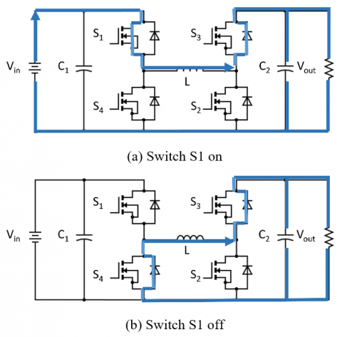
According to Table 1, buck operation in the forward direction requires S1 as the switching device while all the other switches are turned off. Figure 2 shows the power flow direction while S1 is switching. When S1 is on, (Figure 2a), the battery provides power to the inductor L and load. When S1 turns off, (Figure 2b), the antiparallel diode of S4 is forward biased and the inductor provides energy to the load.
This mode of operation results in the fundamental buck topology which, can be designed according to the procedure in the [28]. For continuous conduction mode (CCM), the minimum inductor and capacitor values are given by:
$L_{\text {min }}=\frac{R_L\left(1-D_{\min }\right)}{2 f_s}$ (1)
$C_{\text {min }}=\frac{D_{\max }}{2 f_s r_c}$ (2)
where, $D_{\min }$ and $D_{\max }$ are the minimum and maximum duty cycles, $f_s$ is the switching frequency, $R_L$ is the load resistance and $r_c$ is the equivalent series resistance of the output filter capacitor. The well-known DC static voltage gain for the buck converter is:
$\frac{V_{\text {out }}}{V_{\text {in }}}=D$ (3)
Figure 2. Buck mode of operation
2.2 Boost mode
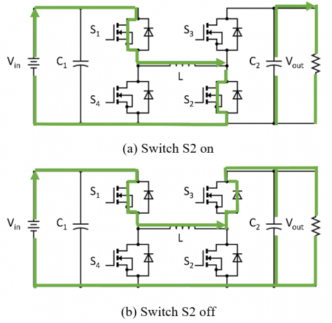
For the boost mode of operation, Figure 3 shows the power flow during the switching of S2. According to Table 1, S1 is on, while S3 and S4 remain off all the time. When S2 is on, Figure 3a, the battery charges the inductor L while the output capacitor $C_2$ provides energy to the load. When S2 is off, Figure 3b, the battery provides energy to both the inductor and the load.
Figure 3. Boost mode of operation
Again, the circuit becomes the fundamental boost topology which can be designed with the procedure in the study [28]. The minimum inductor L and output filter capacitor $C_2$ values for CCM are given by:
$L_{\text {min }}=\frac{2}{27} \frac{R_L}{f_s}$ (4)
$C_{\text {min }}=\frac{D_{\text {max }} V_{\text {out }}}{f_s R_L V_{C p p}}$ (5)
where, $V_{C p p}$ is the maximum peak-to-peak value of the voltage across the output filter capacitance $C_2$. The DC static voltage gain for the boost converter:
$\frac{V_{\text {out }}}{V_{\text {in }}}=\frac{1}{(1-D)}$ (6)
2.3 Component selection
With Eqs. (1)-(4), the minimum values for the passive components in buck and boost modes were calculated. It can be observed how the value of the switching frequency $f_s$ is inversely proportional to all the component values. Then, higher switching frequency results in smaller passive components thus reducing the overall size of the converter. The value of the switching frequency $f_s=500 \mathrm{kHz}$ is selected from the existing WBG devices already available that are EV capable, specifically, the IMZ120R045M1 SiC MOSFET's [29]. Since the converter is required to work in buck and boost modes, the minimum values that met the specifications for both sections were selected. Table 2 shows the parameter values for the components of the bidirectional DC-DC converter. A high switching frequency was selected to take into consideration the higher operating frequencies of WBG devices. Also, the operating power of 13 kW is within the SAE J1772 AC Level 2 and DC Level 1 for EV charging levels [30].
Table 2. Bidirectional DC-DC Converter parameters
|
Parameter |
Value |
|
$R_L$ |
$13 \Omega$ |
|
L |
$10 \mu \mathrm{H}$ |
|
$C_{1,2}$ |
$20 \mu \mathrm{F}$ |
|
$V_{\text {in }}$ |
400 |
|
$V_{\text {out }}$ |
200-750VDC |
|
$f_s$ |
500kHz |
|
P |
13kW |
3.1 Open-loop analysis
DC-DC power converters are nonlinear time-variant systems. Conventional control techniques are intended for Linear Time-Invariant (LTI) systems. Then, to apply these techniques to power converters, simplified models can be developed. The procedure involves deriving a nonlinear average model that captures the general dynamics of the system. Next, linearization under small-signal excitation is obtained. Finally, conversion into the s-domain results in the power stage transfer functions [31]. The transfer function of an LTI system is the ratio of its output to its input in the s-domain. Conventional control designs such as root-locus, frequency-response or PID can be implemented once the transfer function of the small-signal model system has been obtained [32]. The small-signal transfer function of control-to-output for the buck and boost converters are [31]:
$G_{v d B u c k}=\frac{v(s)}{d(s)}=V_{i n} \frac{1}{1+\frac{L}{R} s+L C s^2}$ (7)
$G_{v d B o o s t}=\frac{V_{\text {in }}}{(1-D)} \frac{1-\frac{L_S}{R(1-D)^2}}{1+\frac{L}{R(1-D)^2} s+\frac{L C}{(1-D)^2} s^2}$ (8)
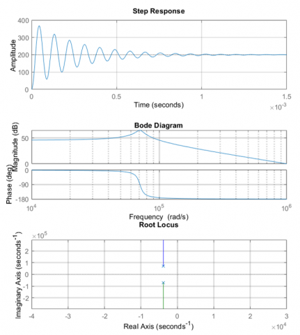
where, $D$ is the duty cycle, and $L, R, C$ are the values from Table 2. The open-loop response to a step input for the buck converter with $D=0.5$ is shown in the top chart of Figure 4. A large initial overshot with a peak voltage of $367 \mathrm{VDC}$ is observed. Under damped response with a settling time of $0.397 \mathrm{~ms}$ is also observed. Also in the figure, the middle chart is the bode diagram and the lower section is the root locus.
Figure 4. (Top) step response, (middle) bode diagram and (bottom) root locus for buck converter with $D=0.5$
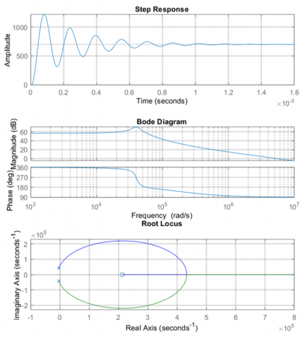
Figure 5. (Top) step response, (middle) bode diagram and (bottom) root locus for boost converter with $D=0.5428$
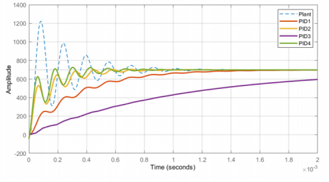
Figure 5 shows the open-loop step response for the Boost converter with the parameters from Table 2 and $D=0.5428$. The voltage overshot reaches a peak voltage of 1220 VDC with an under-damp response and a settling time of $1.02 \mathrm{~ms}$. The Right Half Plane (RHP) zero from the transfer function can be observed in the lower chart of the figure. Its effect is shown in the large drop in the system phase, which fails to reach a steady value. Then, the boost converter is considered a non-minimum phase system.
3.2 Closed-Loop analysis
PID is the elementary control method and is defined by [32]:
$G_{P I D}=\frac{U(s)}{E(s)}=K_p\left(1+\frac{1}{T_i s}+T_d s\right)$ (9)
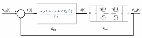
where, $U(s)$ is the output of the controller, $E(s)$ is the difference between the desired and the actual output, $K_p, T_i$, and $T_d$ are the proportional gain, integral time, and derivative time, respectively. The block diagram of the closed-loop control with PID is shown in Figure 6. For the system in the figure, the transfer function is defined,
$\frac{V_{\text {out }}(s)}{V_{\text {ref }}(s)}=\frac{G_{P I D} G_{v d}}{1+G_{P I D} G_{v d}}$ (10)
Figure 6. Block diagram of closed-loop PID control
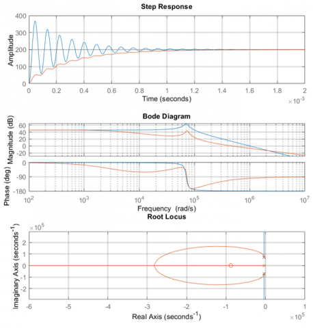
The objective of PID design is to compensate the output of the converter transfer function to obtain the desired dynamic response. Different approaches have been proposed for this objective: Zielger-Nichols method [23], polynomial fitting [20] and software algorithms [33]. The advantage of the last approach is the ability to easily compare multiple scenarios to select the optimal control. For this work, frequency analysis and pole-zero adjustment with software algorithms are implemented for PID tuning. By adjusting the crossover frequency of the system, its transient response can be regulated. Also, the pole-zero of the $G_{P I D}$ can be set to adjust the location of initial $G_{v d}$. Figure 7 shows the PID compensated output of the system compared with the initial output of the buck converter. The resultant PID and transfer function are:
$P I D_{\text {Buck }}=0.000397+17.4 * \frac{1}{s}+2.26 * 10^{-9} s$ (11)
$G_{\text {Buck }}=\frac{9.038 * 10^{-5} s^2+15.88 s+6.972 * 10^5}{2 * 10^{-10} s^3+1.99 * 10^{-6} s^2+1.079 s+3486}$ (12)
From the step response, it can be observed that the peak voltage overshoot has been eliminated and the settling time is now $1.2 \mathrm{~ms}$. Also, the oscillatory behaviour of the converter has been greatly reduced.
The PID and closed-loop transfer function for the Boost converter are,
$P I D_{\text {Boost }}=0.000113+4.28 * \frac{1}{s}+7.48 * 10^{-10} s$ (13)
$G_{\text {Boost }}=\frac{-1.7 * 10^{-9} s^3+10^{-4} s^2+45.5 s+2 * 10^6}{6 * 10^{-10} s^3+5 * 10^{-6} s^2+1.1 s+2995}$ (14)
Figure 7. (Top) step response, (middle) bode diagram and (bottom) root locus for buck converter with $D=0.5$
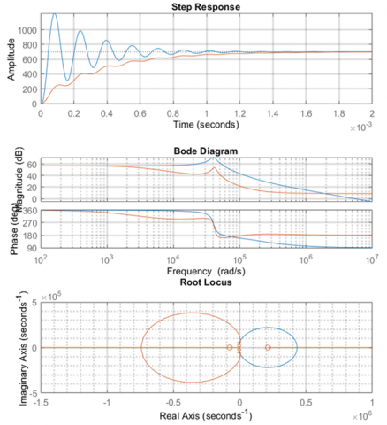
Figure 8. (Top) step response, (middle) bode diagram and (bottom) root locus for boost converter with $D=0.428$
Figure 8 shows the step, bode and pole-zero responses of the close-loop boost converter compared to the initial output. The overshoot has been completely eliminated. However, the settling time has increased to $1.36 \mathrm{ms}$. Also from the figure, the frequency response shows how the PID compensation allowed the converter to reach a minimum phase. Still, a zero in the RHP remains which prevents the system from reaching faster transient responses.
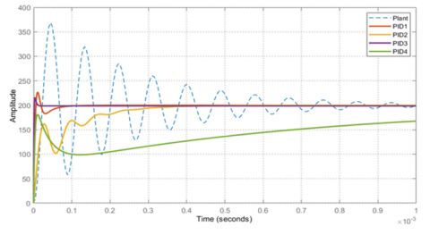
Table 3 and Table 4 summarize the rise time, settling time, overshoot, gain margin and phase margin obtained from four possible PID scenarios for buck and boost operating modes, respectively. Each scenario was obtained by modifying the crossover frequency of the system. This results in different values for the $K_p, T_i$, and $T_d$ parameters from Eq. (9). The top and middle sections of Figures 7 and 8 show that changing the frequency response of the system also changes its transient response. Smaller rise and settling times result in faster transient response but also tend to have voltage overshoot. Scenario PID3 presents the fastest transient response with a high phase margin. However, the slower scenario PID4 presents the highest phase margin without overshoot.
Table 3. Comparison of PID tuning - buck operating mode
|
Parameter |
PID1 |
PID2 |
PID3 |
PID4 |
|
Rise Time (s) |
$4.4 * 10^{-6}$ |
0.00016 |
$9.7 * 10^{-7}$ |
$8* 10^{-6}$ |
|
Settling Time (s) |
$7.1 * 10^{-6}$ |
0.00034 |
$8 * 10^{-6}$ |
0.0025 |
|
Overshoot (%) |
13.2 |
0 |
7.63 |
0 |
|
Gain Margin (dB) |
Inf |
Inf |
Inf |
Inf |
|
Phase Margin (deg) |
69.8 |
49.3 |
83.4 |
89.4 |
Table 4. Comparison of PID tuning - boost operating mode
|
Parameter |
PID1 |
PID2 |
PID3 |
PID4 |
|
Rise Time (s) |
0.0008 |
0.0002 |
0.0023 |
0.00015 |
|
Settling Time (s) |
0.00139 |
0.00067 |
0.00411 |
0.00063 |
|
Overshoot (%) |
0 |
1 |
0 |
4 |
|
Gain Margin (dB) |
11.1 |
26.7 |
18.1 |
24.1 |
|
Phase Margin (deg) |
92.9 |
29.8 |
90 |
24.2 |
Figure 9. Step response of initial buck converter design (blue line) and after PID tuning (PID1,2,3,4)
Figure 10. Step response of initial boost converter design (blue line) and after PID tuning (PID1,2,3,4)
For ease of comparison, the step response of the four scenarios in the buck operating mode are displayed in Figure 9. The open loop step response of the buck converter is also shown (dashed blue line). All the scenarios are stable with high gain and phase margins. For the boost operating mode, scenarios 2 & 4 show the fastest transient responses. However, with voltage overshoot. Scenarios 1 & 3 have slower transients but high phase margin and zero overshot. Figure 10 shows the open loop step response of the boost converter (dashed blue line) and the four closed loop scenarios from the table.
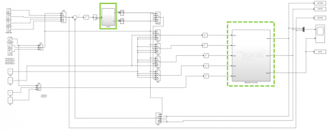
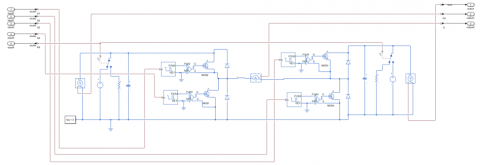
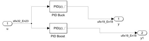
The bidirectional circuit topology and PID control from the previous sections were simulated in Matlab/Simulink. The top section of Figure 11 shows the block diagram of the bidirectional converter in a closed loop with the PID controllers for the buck and boost modes. Also, the necessary control signals to select the four modes of operation are included. The middle section of Figure 11 shows the circuit topology implemented with Simscape. To include WBG features into the simulations, IMZ120R045M1 SiC MOSFET's were used for the implementation with PWM switching frequency set at 500 kHz [29]. Individual drivers and PWM modulators were configured for each power switch. The bottom section of Figure 11 presents the PID control modules for the buck and boost modes of operation. Scenarios PID4 and PID1 from Tables 3 & 4 were selected for the buck and boost modes, respectively. The fixed-point conversion was performed to prepare the control blocks for FIL validation.
(a) Block diagram in Simulink
(b) Circuit topology in Simscape (dashed square top figure)
(c) Control block for FIL simulation
Figure 11. Bidirectional converter in closed-loop with PID
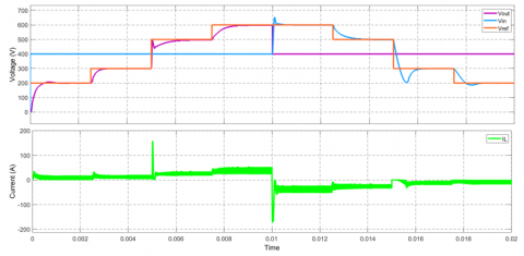
Figure 12 shows the simulation results for bidirectional operation in buck and boost modes. Step-up and step-down modes of operation can be observed in the forward direction. Then, at time 10 ms, buck and boost operation in the reverse direction is observed: Current direction, input and output voltage are reversed. The rise and settling times and voltage overshoot for the four modes of operation are summarized in Table 5 for the buck mode and Table 6 for the boost mode.
Figure 12. PID control of bidirectional converter in boost and buck modes
Table 5. Summary of FPGA-in-the-loop control performance-Buck operating mode
|
Parameter |
Forward |
Reverse |
||
|
Rise Time (s) |
$3.1 * 10^{-4}$ |
$3.2 * 10^{-4}$ |
$2.3 * 10^{-4}$ |
$3.7* 10^{-4}$ |
|
Settling Time (s) |
$9.5* 10^{-4}$ |
$7 * 10^{-4}$ |
$1.2* 10^{-4}$ |
$1.1 * 10^{-4}$ |
|
Vref (V) |
200 |
300 |
300 |
200 |
|
Peak (V) |
207.3 |
299.8 |
203 |
187 |
|
Overshoot (%) |
3.65 |
0 |
48.5 |
13 |
|
$\Delta V$ |
200 |
100 |
200 |
100 |
Table 6. Summary of FPGA-in-the-loop control performance-Boost operating mode
|
Parameter |
Forward |
Reverse |
||
|
Rise Time (s) |
$3.6 * 10^{-5}$ |
$8 * 10^{-4}$ |
$4 * 10^{-5}$ |
$7 * 10^{-4}$ |
|
Settling Time (s) |
$1.6 * 10^{-3}$ |
$1.5 * 10^{-3}$ |
$4.2 * 10^{-4}$ |
$1.1* 10^{-3}$ |
|
Vref (V) |
500 |
600 |
600 |
500 |
|
Peak (V) |
498 |
599 |
652 |
500.5 |
|
Overshoot (%) |
0 |
0 |
26 |
0 |
|
$\Delta V$ |
200 |
100 |
200 |
100 |
4.1 FPGA-in-the-loop (FIL)
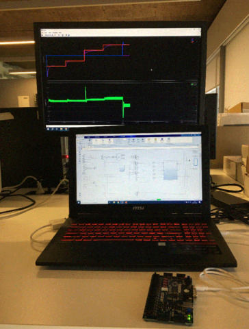
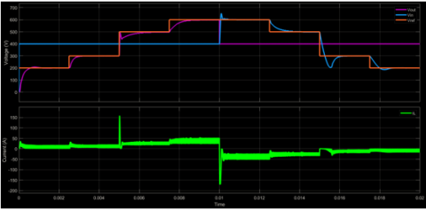
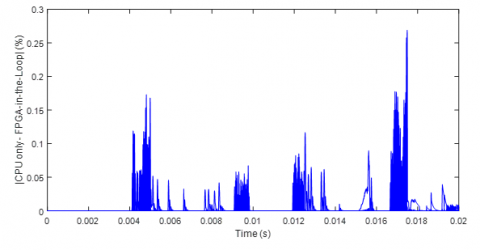
For FIL validation, HDL code was generated following the procedure in the study [34]. Then, an interface was created to communicate between the simulation and the FPGA [35]. The PID control blocks shown in the top and bottom sections of Figure 11 were replaced by the FIL interface. Figure 13 shows the laboratory setup with the computer simulation interfacing with the PID implemented in the FPGA. A Xilinx Artix-7 (XC7A35T-1CPG236C) device was used for this work. Figure 14 shows the simulation results with the FIL setup. To validate the FIL simulation, Figure 15 shows the absolute percentage difference between the CPU simulation only and the FGPA-in-the-loop approach. For both cases, the DC-DC converter is simulated with double-precision floating-point 64-bit word data type while the data for the control block is converted to fixed-point data type. The lower section of Figure 11 shows the different types of data used within the block, i.e., sfix32_En23 stands for signed fixed-point with word length of 32 bits and fraction length of 23 bits. The data can be signed $s$, or unsigned $u$. It can be observed in Figure 15 that at any given time, the maximum absolute difference is less than 0.3%. Also from the figure, it can be validated that the parameters from Tables 5 and 6 also hold for the FIL setup.
From Table 5, the settling time measured in the buck forward mode of operation is in the order of fractions of milliseconds with almost zero overshoot. Higher switching frequencies have been linked to faster transient responses [24]. Table 6 shows that the settling time in the boost forward mode of operation is slightly larger than in the boost mode: a slower system response ensured stable operation of the system. The lower section of Figure 14 shows the current of the converter in the desired CCM during forward (positive) and reverse (negative) operation. Future work will focus on reducing the large overshoot observed when transitioning from boost mode to buck mode in reverse mode of operation.
Reference [20] reports settling times in the order of $10^{-3}$ s for a buck converter with FIL, input voltage of 24 VDC and switching frequency of 48 kHz. Similarly, Liu et al. [21] report an FPGA-MPC control for a buck converter with 12 VDC input voltage and settling times also in the order of $10^{-3}$ s. In the study [22], PI was FPGA implemented for a DAB converter with 1.1kV voltage rating and switching frequency also in the kHz range. PI control for a bidirectional boost-buck converter is FPGA implemented in the study [23] with 20kHz switching frequency and input/output voltage of 288/450 VDC. Therefore, the contribution of this work is to present the design and FPGA-in-the-loop validation of a PID control algorithm for a bidirectional converter with four modes of operation, 400 VDC input voltage and 500 kHz switching frequency. Then, providing WBG device capability and FIL validation at voltage rating levels of EV applications.
Figure 13. Laboratory setup for FIL bidirectional converter control validation
Figure 14. FIL bidirectional converter and control validation
Figure 15. Absolute difference (in percentage) between the simulation with CPU only and FIL simulation
In this work, a bidirectional converter with voltage overlapping and buck-boost operation has been designed. Electric vehicle ratings were used for component design with an input voltage of 400 VDC, an output voltage of 200 VDC up to 750 VDC and power rating of 13 kW which is within the SAE J1772 AC Level 2 and DC Level 1 for EV charging levels. The wide output voltage range is a desired feature in converters that interface between the battery and the propulsion motor. WBG devices were taken into account for the design with a switching frequency of 500 kHz, not being possible for Si devices. Passive component’s dimensions in a DC-DC converter are inversely proportional to the switching frequency; then, by increasing the switching frequency above the levels allowed by traditional Si devices, reduction in the size of the components was achieved. Independent PID control was implemented in buck and boost modes of operation with power flowing in forward and reverse modes. The control algorithm was validated through FIL methodology which is an efficient procedure to accelerate algorithm development by bringing the design a step closer to product manufacturing. Traditional Hardware-in-the-Loop (HIL) validation requires expensive devices to simulate in real-time the plant model while the control algorithm is allocated in a DSP or microcontroller. The FIL methodology applied ensures the algorithm is hardware-validated in a closed loop with a high-fidelity model of the plant running in the computer. Then, FIL is a cost-effective approach for control algorithms validation. PID is the benchmark control for industrial applications of power converters. Then, this design will serve as a baseline for comparison of the real effectiveness of other existing methods in the literature.
This work was supported by the Consejo Nacional de Humanidades, Ciencia y Technología (CONAHCyT)-México, and the Intelligent Systems program from UDLAP in collaboration with the Universitat de València, Spain.
[1] EPA. Global Greenhouse Gas Emissions Data. Retrieved February 9, 2023, from https://www.epa.gov/ghgemissions/global-greenhouse-gas-emissions-data.
[2] NASA-JPL. Causes | Facts – Climate Change: Vital Signs of the Planet. Retrieved February 9, 2023, from https://climate.nasa.gov/causes.
[3] European Environment Agency. Air Pollutant Emissions — European Environment Agency. Retrieved February 9, 2023, from https://www.eea.europa.eu/airs/2018/environment-and-health/air-pollutant-emissions.
[4] Safayatullah, M., Elrais, M.T., Ghosh, S., Rezaii, R., Batarseh, I. (2022). A comprehensive review of power converter topologies and control methods for electric vehicle fast charging applications. IEEE Access, 10: 40753-40793. https://doi.org/10.1109/ACCESS.2022.3166935
[5] Khaligh, A., D’Antonio, M. (2019). Global trends in high-power on-board chargers for electric vehicles. IEEE Transactions on Vehicular Technology, 68(4): 3306-3324. https://doi.org/10.1109/TVT.2019.2897050
[6] Xuan, Y., Yang, X., Chen, W., Liu, T., Hao, X. (2021). A novel three-level CLLC resonant DC-DC converter for bidirectional EV charger in DC microgrids. IEEE Transactions on Industrial Electronics, 68(3): 2334-2344. https://doi.org/10.1109/TIE.2020.2972446
[7] Heydari-doostabad, H., O’Donnell, T. (2022). A wide-range high-voltage-gain bidirectional DC–DC converter for V2G and G2V hybrid EV charger. IEEE Transactions on Industrial Electronics, 69(5): 4718-4729. https://doi.org/10.1109/TIE.2021.3084181
[8] Suresh, K., Bharatiraja, C., Chellammal, N., Tariq, M., Chakrabortty, R.K., Ryan, M.J., Alamri, B. (2021). A multifunctional non-isolated dual input-dual output converter for electric vehicle applications. IEEE Access, 9: 64445-64460. https://doi.org/10.1109/ACCESS.2021.3074581
[9] Jiao, T., Zhang, X.N., Wang, B.F., Cui, G.Q., Ma, W.Z. (2021). A multiple-port three-level DC/DC converter for HESS with power sharing in DC microgrids. Chinese Journal of Electronics, 30(3): 570-583. https://doi.org/10.1049/cje.2021.04.011
[10] Parvez, M., Pereira, A.T., Ertugrul, N., Weste, N.H.E., Abbott, D., Al-Sarawi, S.F. (2021). Wide bandgap DC–DC converter topologies for power applications. Proceedings of the IEEE, 109(7): 1253-1275. https://doi.org/10.1109/JPROC.2021.3072170
[11] Jin, F., Nabih, A., Chen, C., Chen, X., Li, Q., Lee, F.C. (2021). A high efficiency high density DC/DC Converter for battery charger applications. In 2021 IEEE Applied Power Electronics Conference and Exposition (APEC), Phoenix, AZ, USA, pp. 1767-1774. https://doi.org/10.1109/APEC42165.2021.9487108
[12] Ulrich, L. (2022). 800-Volt EV Charging: The Other Palliative for Range Anxiety. IEEE Spectrum. Retrieved October 23, 2022, from https://spectrum.ieee.org/ev-charging-800-volt.
[13] Moradisizkoohi, H., Elsayad, N., Mohammed, O.A. (2021). A voltage-quadrupler interleaved bidirectional DC-DC converter with intrinsic equal current sharing characteristic for electric vehicles. IEEE Transactions on Industrial Electronics, 68(2): 1803-1813. https://doi.org/10.1109/TIE.2020.2998757
[14] Gorji, S.A., Sahebi, H.G., Ektesabi, M., Rad, A.B. (2019). Topologies and control schemes of bidirectional DC–DC power converters: An overview. IEEE Access, 7: 117997-118019. https://doi.org/10.1109/ACCESS.2019.2937239
[15] Luo, P., Wang, D., Peng, X. (2019). An adaptive voltage scaling buck converter with preset circuit. Chinese Journal of Electronics, 28(2): 229-236. https://doi.org/10.1049/cje.2019.01.007
[16] Li, T.Y., Zhang, F., Guo, W., Sun, M., Chen, L. (2021). A survey: FPGA-Based dynamic scheduling of hardware tasks. Chinese Journal of Electronics, 30(6): 991-1007. https://doi.org/10.1049/cje.2021.07.021
[17] Xiyuan, P., Jinxiang, Y., Bowen, Y., Liansheng, L., Yu, P. (2021). A review of FPGA-Based custom computing architecture for convolutional neural network inference. Chinese Journal of Electronics, 30(1): 1-17. https://doi.org/10.1049/cje.2020.11.002
[18] Frances-Villora, J.V., Bataller-Mompean, M., Mjahad, A., Rosado-Munoz, A., Gutierrez Martin, A., Teruel-Marti, V., Villanueva, V., Hampel, K.G., Guerrero-Martinez, J.F. (2020). Real-time localization of epileptogenic foci EEG signals: An FPGA-based implementation. Applied Sciences, 10(3): 827. https://doi.org/10.3390/app10030827
[19] Ządek, P., Koczor, A., Gołek, M., Matoga, Ł., Penkala, P. (2015). Improving efficiency of FPGA-in-the-loop verification environment. IFAC-PapersOnLine, 48(4): 180-185. https://doi.org/10.1016/j.ifacol.2015.07.029
[20] Zurita-Bustamante, E.W., Linares-Flores, J., Guzmán-Ramírez, E., Sira-Ramírez, H. (2011). A comparison between the GPI and PID controllers for the stabilization of a DC-DC 'buck' converter: A field programmable gate array implementation. IEEE Transactions on Industrial Electronics, 58(11): 5251-5262. https://doi.org/10.1109/TIE.2011.2123857
[21] Liu, Z., Xie, L., Bemporad, A., Lu, S. (2018). Fast linear parameter varying model predictive control of buck DC-DC converters based on FPGA. IEEE Access, 6: 52434-52446. https://doi.org/10.1109/ACCESS.2018.2869043
[22] Watson, A.J., Wheeler, P.W., Clare, J.C. (2011). Field programmable gate array based control of Dual Active Bridge DC/DC Converter for the UNIFLEX-PM project. In Proceedings of the 2011 14th European Conference on Power Electronics and Applications, Birmingham, UK, pp. 1-9.
[23] Ali, A., Faisal, N., Zia, Z., Makda, I., Usman, A. (2022). Rapid prototyping of bidirectional DC-DC converter control using FPGA for electric vehicle charging applications. In 2022 IEEE 13th International Symposium on Power Electronics for Distributed Generation Systems (PEDG), Kiel, Germany, pp. 1-6. https://doi.org/10.1109/PEDG54999.2022.9923288.
[24] Martinez-Vera, E., Banuelos-Sanchez, P. (2024). Review of bidirectional DC-DC converters and trends in control techniques for applications in electric vehicles. IEEE Latin America Transactions, 22(2): 144-155. https://doi.org/10.1109/TLA.2024.10412031
[25] Martínez-Vera, E., Bañuelos-Sanchez, P., Etcheverry, G. (2023). Comparative examination of control strategies in DC-DC power converters: A traditional and artificial intelligence perspective. Journal of Intelligent Systems and Control, 2(2): 82-98. https://doi.org/10.56578/JISC020203
[26] Khan, M.A., Ahmed, A., Husain, I., Sozer, Y., Badawy, M. (2015). Performance analysis of bidirectional DC-DC converters for electric vehicles. IEEE Transactions on Industrial Applications, 51(4): 3442-3452. https://doi.org/10.1109/TIA.2015.2388862
[27] Caricchi, F., Crescimbini, F., Capponi, F.G., Solero, L. (1998). Study of bi-directional buck-boost converter topologies for application in electrical vehicle motor drives. In APEC '98 Thirteenth Annual Applied Power Electronics Conference and Exposition, Anaheim, CA, USA, pp. 287-293. https://doi.org/10.1109/APEC.1998.647705
[28] Kazimierczuk, M.K. (2015). Pulse-width modulated DC-DC power converters. John Wiley & Sons. https://doi.org/10.1002/9781119009597
[29] Infineon Technologies. IMZ120R045M1. Retrieved June 9, 2023, from https://www.infineon.com/cms/en/product/power/mosfet/silicon-carbide/discretes/imz120r045m1.
[30] SAE International. (2017). J1772 Electric Vehicle and Plug in Hybrid Electric Vehicle Conductive Charge Coupler. Retrieved June 27, 2020, from https://www.sae.org/standards/content/j1772_201710.
[31] Choi, B. (2013). Pulsewidth modulated DC-to-DC power conversion. John Wiley & Sons, Inc. https://doi.org/10.1002/9781118772188
[32] Ogata, K. (2010). Modern control engineering. prentice hall. Retrieved from https://books.google.com.mx/books?id=Wu5GpNAelzkC.
[33] Mathworks. PID Tuning Algorithm - MATLAB & Simulink. Retrieved April 6, 2023, from https://www.mathworks.com/help/control/getstart/pid-tuning-algorithm.html.
[34] Mathworks. HDL Coder Documentation. Retrieved February 15, 2023, from https://www.mathworks.com/help/hdlcoder/index.html?s_tid=hc_product_card.
[35] Mathworks. FPGA-in-the-Loop Simulation - MATLAB & Simulink. Retrieved February 15, 2023, from https://www.mathworks.com/help/hdlverifier/ug/fpga-in-the-loop-fil-simulation.html.