Haider Al-Mumen![]()
© 2023 IIETA. This article is published by IIETA and is licensed under the CC BY 4.0 license (http://creativecommons.org/licenses/by/4.0/).
OPEN ACCESS
This research delves into the design, simulation, and evaluation of a high-sensitivity, swift-response single-axis Micro-Electro-Mechanical Systems (MEMS) accelerometer, inspired by the intricate design of a spider web. The accelerometer, characterized by a circular silicon structure of 1mm radius, embraces a proof mass with a radius and thickness of 60 µm and 2 µm, respectively. A comprehensive study was undertaken to scrutinize the electrical properties, notably the time response, and mechanical properties, specifically the stress effects on the device. An outstanding sensitivity of 0.047 µm/g and a brisk rise time of 0.1 ms within the acceleration range of -50 to 50 g were observed. A signal conditioning and processing circuit, composed of a bridge circuit, two operational amplifiers functioning as a difference amplifier, and a filter, was meticulously designed using MATLAB and integrated with the accelerometer sensor, facilitating the derivation of a DC output voltage representative of the sensed acceleration. The simplicity, ease of modification, swift response, and high sensitivity of the proposed MEMS accelerometer underscore its promising application potential.
Micro-Electro-Mechanical Systems (MEMS), sensor, accelerometer, spider web-like, simulation, signal conditioning
Recent years have seen significant strides in the realm of MEMS technology, along with micro and nanotechnology [1-17]. The surge in research interest can be attributed to the compact size and minimal energy consumption of these systems [18]. Further bolstering their popularity, they find prolific applications, notably in sensor technology and communication devices [19-22].
A MEMS accelerometer, a device that detects acceleration with remarkable sensitivity and precision, exemplifies this technological advancement. Its capability to sense movement along one or multiple axes depending on its application is particularly noteworthy. Contemporary usage of MEMS accelerometers extends to cellphones, where they detect angular displacement to adjust screen orientation based on device positioning [23]. Other applications span the aerospace and military sectors, where the need for precise and reliable measurement tools is paramount [24, 25].
Various MEMS accelerometer designs have been reported, with moving finger structures being the most prevalent [26, 27]. The fundamental principle of acceleration sensing in these structures is the fluctuation of capacitance value between the fingers. Yet, alternative techniques have been developed that primarily rely on piezoelectric [28, 29] and piezoresistive [30, 31] variations within the accelerometer. An optical-based MEMS accelerometer has also been proposed, aimed at achieving heightened sensing resolution [32].
In this study, a novel spider web-like accelerometer of microscale dimensions was designed, simulated, and evaluated. The device specifications were deliberately chosen to showcase its robustness in terms of size, sensitivity, and response time. Notably, compared to other designs reported in the literature, this accelerometer is straightforward in its structure and can be altered with ease, further underscoring its potential for a variety of applications.
2.1 Proof mass
The proof mass was designed to be has a circular shape. The volume of the proof mass can be calculated by:
$V=r^2 * \pi^* h$ (1)
where,
r is the radius of the proof mass,
h is the thickness of the proof mass, and
V is the volume of the proof mass, which is determined as, V=22.608*10-15 m3.
$m=\rho . V$ (2)
where,
m is the mass of proof-mass, and
ρ is the density of Si, which is determined as, m=52.451*10-9 g.
2.2 The initial force acts on the proof mass
$F=m * a$ (3)
which is determined as, F=0.513*10-9 N. While the force subjected to each beam is, Fbeam=F/8=0.064*10-9 N.
2.3 Beams deflection
The theoretical value of the beam deflection (spider thread) is,
$\delta=\frac{\mathrm{F}_{\text {beam }} * L_{\text {beam }}^3}{12 E I}$ (4)
where,
W is the width of the beam. Then, $\delta=0.047$ µm at the acceleration of 1 g.
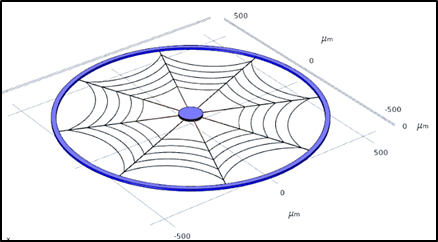
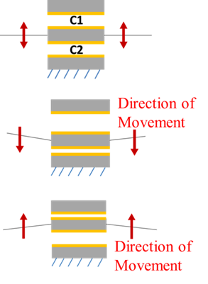
As in Figure 1(a), the MEMS accelerometer has 8 sectors, each sector consists of two beams with five spider threads suspending on them. The device has a diameter of 500 µm. The spider threads are in a curvature shape, which is like the spider home so that they can vibrate easily leading to increasing the device sensitivity. Specifically, as the structure dimension increased (beams and threads), which is easy to achieve, the sensitivity to the external acceleration would be increased. Of course, there is a limitation for that, first, because the device needs to be in the microscale dimension, and second, probably the overall device mass would elevate causing a decline in sensitivity or even structural collapse. The structure of the device is made of gold layer on the top of the surface of a Si substrate, as in Figure 1(b). Two capacitors then constructed (C1 and C2). As an external vibration is applied, the device starts vibration in up and down directions. This vibration leads to a variation in the capacitor’s values. These variations in the capacitors are proportional to the acceleration values, which can be measured and converted to a DC output, as will be explained in the next sections.
(a) The device structure
(b) The concept of measurement
Figure 1. The spider web-like design
4.1 Acceleration vs. capacitance
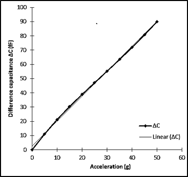
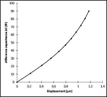
Based on our design, the air gap between movable finger and fixed finger was made to be 1 µm. The measured capacitance at 0 g is equal to ΔC=0. When the applied acceleration elevates from 0 g to 50 g step 5 g, the capacitance changes from 0 to 90 Ff (Table 1). Specifically, the variations in the air gap causes increasing in capacitance in one side whereas decreasing in capacitance in the other side and then ΔC will be generated. Figure 2(a) shows the capacitance difference versus applied acceleration. While Figure 2(b) displays the displacement versus capacitance difference. The relationship is approximately linear, which means that there is no need for linearization or lookup table to obtain the measurement and then the measurement error is negligible. Basically, Linearity is one of the significant factors that must be taken into account when designing a sensor. The sensitivity of the device was also obtained by measuring the difference between the two capacitors of the device divided by the acceleration difference. The device sensitivity was measured to be around 2 Ff.
(a) Acceleration vs. capacitance variation' s
(b) Displacement vs. capacitance
Figure 2. The device characteristic
Table1. Acceleration vs. capacitance difference
|
Acceleration (g) |
Displacement (µm) |
C2 (Ff) |
C1(Ff) |
ΔC(Ff) |
|
0 |
0 |
50.1 |
50.1 |
0 |
|
5 |
0.218 |
56.235 |
45.171 |
11.063 |
|
10 |
0.405 |
62.836 |
41.656 |
21.179 |
|
15 |
0.558 |
69.497 |
39.167 |
30.329 |
|
20 |
0.684 |
76.183 |
37.321 |
38.861 |
|
25 |
0.792 |
82.968 |
35.884 |
47.083 |
|
30 |
0.885 |
89.945 |
34.719 |
55.226 |
|
35 |
0.969 |
97.207 |
33.746 |
63.461 |
|
40 |
1.044 |
104.843 |
32.914 |
71.929 |
|
45 |
1.112 |
112.946 |
32.189 |
80.757 |
|
50 |
1.176 |
121.614 |
31.548 |
90.066 |
4.2 Bending stress
(a) The bending stress at the terminal of the beams vs. acceleration
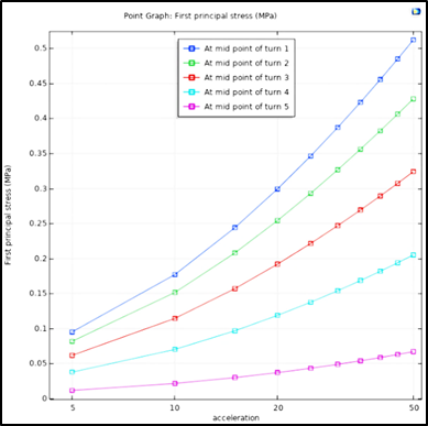
(b) Bending stress at midpoint of the turns vs. acceleration
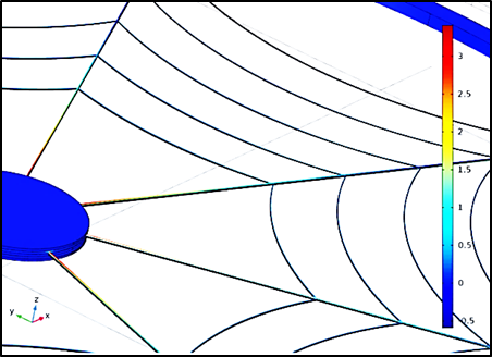
(c) The stress profile
Figure 3. The bending stress
Stress in the beams occurs when acceleration is applied to the accelerometer. Basically, the stress is distributed irregularly. In a certain area, the stress is relatively high while it is relatively low in others, which is according to the shape of the beams and the direction of acceleration. Calculating the maximum stress and stress profile is important to avoid device collapse. Each part of the device has a certain level of stress. The model must be designed so that the maximum stress due to acceleration is less than the maximum stress that the material can withstand (UTS). For silicon material UTS is 7000 MPa. At acceleration of 50 g, the stress is about 2.45 MPa at the point of contact of the beam with the proof mass, while it is about 2.1 MPa at the point of contact of the beam with the anchor (Figure 3(a)). The Bending Stress at midpoint of the turns (1 to 5) versus the acceleration is shown in Figure 3(b). Additionally, the bending profile is displayed in Figure 3(c). The maximum stress was observed at the beam to proof mass contact.
4.3 Time response
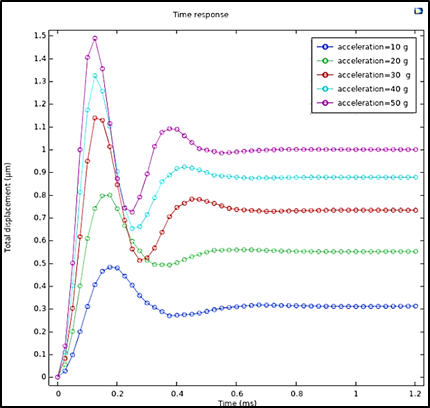
(a) Time response of the device at radius r=60
(b) Time response of the device at r=50
(c) Time response of the low acceleration range (0g-1g)
Figure 4. Time response of the device for two different radius and high/low acceleration ranges
The time response of the device was determine to find the dynamic characteristic of the device. The results show that the maximum achieved overshoot was 1.55 µm at 40 g and the corresponding damping ratio was 0.86. While at 20 g, the overshoot was 1.2 µm and the damping ratio was 0.9. Moreover, it was observed that the rise time, which is the best indicator parameter for speed of the response, decreases with acceleration, as in Figure 4. For instant, it was 0.09 ms at 20 g, while it was 0.06 ms at 50 g. A slice change in overshoot and rise time were achieved when R increased from 50 to 60, which is resnable. Furthermore, the device was also tested at low acceleration range (0 g to 1 g), as shown in Figure 5. Therefore, the measuring range of the device was calculated as -50 g to 50 g and the device resolution was 0.05 g.
4.4 Electric circuit design
Building on the fact that the amplitude of the sensed signal is depending on the amount of the acceleration input, a signal conditioning and processing circuits was designed. The sensed signal was considered as an amplitude modulating signal. To obtain an output dc voltage, an amplifier and coherent detector was used. The equivalent electrical circuit of the sensor and the functional block diagram of the circuit is shown in Figure 5.
Figure 5. The functional diagram of the electric circuit that converts the capacitance variation into voltage variations
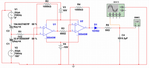
The schematic diagram was designed by MATLAB Simulink for the circuit (Figure 6). It consists of two voltage amplifiers. First amplifier gets the input voltage, which is proportional to the capacitance difference (ΔC), from the ac bridge circuit. The second stage amplifier further increases the voltage level. The output of the second amplifier is connected to a diode, functions as a rectifier which clips the negative part of the sinusoidal signal. Then, diode passes the signal to the RC circuit works as a low pass filter. The filter output is a dc voltage measured by a voltmeter of the MATLAB Simulink, which is represent applied acceleration.
Figure 6. Schematic diagram of the electric circuit which includes signal conditioning and signal processing components
The plot of the output DC voltage versus acceleration is depicted in Figure 7. The linear property of the device indicates that the device can be used as a practical sensor.
Figure 7. Output DC voltage vs. acceleration
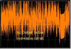
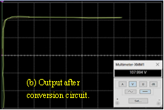
To observe the device output voltage before and after the filter circuit, a 50 g acceleration was applied as an input to the device and then the device output before the filter was measured. The device output was a waveform similar to the amplitude modulation signal, as shown in Figure 8(a). Also, the output voltage in the output of the filter, which is a DC voltage was determined as in Figure 8(b).
Figure 8. The AC sensing voltage at 50 g
This paper presents a design and simulation of a micro-sensor to measure acceleration. The spider-web architecture was used in the designing of this sensor. The designed and simulated were implemented using Comsol simulator. To study the performance of the device, the properties of its time response was studied for low and high acceleration inputs. Moreover, the stress distribution on the device structure was studied as a function of the applied acceleration, the results showed the maximum stress is in the beam-proofmass connection point. In addition, an electronic circuit was designed to convert the acceleration into DC voltage to facilitate reading the acceleration values. The achieved sensitivity for our design is 0.047 µm/g and the rise time is 0.1 ms for the range of -50 to 50 g. The linear property shown by the device will make it candidate for future practical applications.
[1] Al-Mumen, H. (2015). Characterisation of SU-8 n-doping carbon nanotube‐based electronic devices. Micro & Nano Letters, 10(12): 670-673. https://doi.org/10.1049/mnl:20080030
[2] Ghlam, K., Oukli, M. (2023). Performance analysis of rotary electromagnetic micromotors across different size and weight scales. Journal Européen des Systèmes Automatisés, 56(3): 459-463. https://doi.org/10.18280/jesa.560313
[3] Al-Mumen, H., Hamad, A.A. (2022). Design and characterization of an radio frequency reused energy system for nano-devices. Bulletin of Electrical Engineering and Informatics, 11(5): 2595-2602. https://doi.org/10.11591/eei.v11i5.4321
[4] Bégot, S., Getie, M.Z., Diallo, A., Lanzetta, F., Barthès, M., de Labachelerie, M. (2021). A novel model and design of a mems Stirling engine. International Journal of Heat and Technology, 39(4): 1037-1046. https://doi.org/10.18280/ijht.390401
[5] Al-Mumen. H. (2021). Brief review on: Fabrication of single electron nano-devices. University of Thi-Qar Journal for Engineering Sciences, 11(2): 117-121. http://www.doi.org/10.31663/tqujes.11.2.399
[6] Yuan, R.L. (2020). Positioning of wireless sensor network under emergency communication environment. Instrumentation Mesure Métrologie, 19(4): 273-279. https://doi.org/10.18280/i2m.190404
[7] Al-Mumen, H., Rao, F., Dong, L., Li, W. (2012). Characterization of surface heat convection of bilayer graphene. In 2012 12th IEEE International Conference on Nanotechnology (IEEE-NANO), Birmingham, pp. 1-4. https://doi.org/10.1109/NANO.2012.6322100
[8] Arthanareeswaran, J., Karunanidhi, B., Muruganantham, S., Dhamodharan, A., Swarnamma, S.K.C. (2021). Automatic vehicle accident indication and reporting system for road ways using internet of things. International Journal of Safety and Security Engineering, 11(3): 269-277. https://doi.org/10.18280/ijsse.110307
[9] Al-Mumen, H., Li, W. (2018). Complementary metal-SU8-graphene method for making integrated graphene nanocircuits. Micro & Nano Letters, 13(4): 465-468. https://doi.org/10.1049/mnl:20080030
[10] Thao, L.Q., Bach, N.C., Bach, P.X., Hieu, L.P.M.H., Phuc, T.G. (2023). Intelligent health assistant for pupils. Instrumentation Mesure Métrologie, 22(1): 11-19. https://doi.org/10.18280/i2m.220102
[11] E isa, Z., Al-Mumen, H. (2022). Characteristic control of SWCNT-FET by varying its chirality and dimensions. Indonesian Journal of Electrical Engineering and Informatics (IJEEI), 10(3): 698-706. https://doi.org/10.52549/ijeei.v10i3.4046
[12] Ligot, D., Marguet, C., Favre, B., Messaoudi, B., Gervasoni, D., Litaudon, P. (2020). Noninvasive instrumentation for respiratory activity recording in freely moving rats placed a large experimental space. Instrumentation Mesure Métrologie, 19(3): 185-195. https://doi.org/10.18280/i2m.190303
[13] L-Mumen, H. (2016). Optoelectronic properties of dome-shaped substrate UV detector with optical coating. International Journal of Applied Engineering Research, 11(16): 8916-8919.
[14] Abdulateef, A.T., Makki, S.A. (2023). Enhancing indoor navigation accuracy with a smartphone-based pedometer system. Ingénierie des Systèmes d’Information, 28(4): 921-930. https://doi.org/10.18280/isi.280412
[15] Shams, O.A., Alturaihi, M.H., Mustafa, M.A.S., Majdi, H.S. (2023). Enhancement of drones’ control and guidance systems channels: A review. Journal Européen des Systèmes Automatisés, 56(2): 201-212. https://doi.org/10.18280/jesa.560204
[16] Shivanna, P., Venkatesiah, S.S. (2021). Secure multimodal authentication scheme for wireless sensor networks. International Journal of Safety and Security Engineering, 11(6): 653-661. https://doi.org/10.18280/ijsse.110605
[17] Li, T. (2020). Design of an automatic detector for gas desorption of coal samples. Instrumentation Mesure Métrologie, 19(5): 355-361. https://doi.org/10.18280/i2m.190505
[18] Algamili, A.S., Khir, M.H.M., Dennis, J.O., Ahmed, A.Y., Alabsi, S.S., Ba Hashwan, S.S., Junaid, M.M. (2021). A review of actuation and sensing mechanisms in MEMS-based sensor devices. Nanoscale Research Letters, 16: 1-21. https://doi.org/10.1186/s11671-021-03481-7
[19] Prato, A., Mazzoleni, F., D'Emilia, G., Gaspari, A., Natale, E., Schiavi, A. (2021). Metrological traceability of a digital 3-axis MEMS accelerometers sensor network. Measurement, 184: 109925. https://doi.org/10.1016/j.measurement.2021.109925
[20] Yellamma, P., Chandra, N.S.N.S.P., Sukhesh, P., Shrunith, P., Teja, S.S. (2021). Arduino based vehicle accident alert system using GPS, GSM and MEMS accelerometer. In 2021 5th International Conference on Computing Methodologies and Communication (ICCMC), Erode, India, pp. 486-491. https://doi.org/10.1109/ICCMC51019.2021.9418317
[21] Liu, D.S., Wei, S.S., Wang, D.J. (2022). Sensitivity comparison between monolayer graphene and multilayer graphene. Journal of New Materials for Electrochemical Systems, 25(3): 219-223. https://doi.org/10.14447/jnmes.v25i3.a10
[22] Arthanareeswaran, J., Karunanidhi, B., Muruganantham, S., Dhamodharan, A., Swarnamma, S.K.C. (2021). Automatic vehicle accident indication and reporting system for road ways using internet of things. International Journal of Safety and Security Engineering, 11(3): 269-277. https://doi.org/10.18280/ijsse.110307
[23] Kealy, A., Retscher, G. (2017). MEMS and wireless options in cellular phones for user localization. In Proceedings of the ION 2017 Pacific PNT Meeting, Honolulu, Hawaii, pp. 263-275. https://doi.org/10.33012/2017.15060
[24] Dong, Y. (2013). MEMS inertial navigation systems for aircraft. In MEMS for automotive and aerospace applications, pp. 177-219. https://doi.org/10.1533/9780857096487.2.177
[25] Niu, W. (2018). Summary of research status and application of mems accelerometers. Journal of Computer and Communications, 6(12): 215. https://doi.org/10.4236/jcc.2018.612021
[26] He, J., Zhou, W., Yu, H., He, X., Peng, P. (2018). Structural designing of a MEMS capacitive accelerometer for low temperature coefficient and high linearity. Sensors, 18(2): 643. https://doi.org/10.3390/s18020643
[27] Zhou, X., Che, L., Liang, S., Lin, Y., Li, X., Wang, Y. (2015). Design and fabrication of a MEMS capacitive accelerometer with fully symmetrical double-sided H-shaped beam structure. Microelectronic Engineering, 131: 51-57. https://doi.org/10.1016/j.mee.2014.10.005
[28] Tian, B., Liu, H., Yang, N., Zhao, Y., Jiang, Z. (2016). Design of a piezoelectric accelerometer with high sensitivity and low transverse effect. Sensors, 16(10): 1587. https://doi.org/10.3390/s16101587
[29] Le, X., Shi, Q., Vachon, P., Ng, E.J., Lee, C. (2021). Piezoelectric MEMS—evolution from sensing technology to diversified applications in the 5G/Internet of Things (IoT) era. Journal of Micromechanics and Microengineering, 32(1): 014005. https://doi.org/10.1088/1361-6439/ac3ab9
[30] Liu, F., Gao, S., Niu, S., Zhang, Y., Guan, Y., Gao, C., Li, P. (2018). Optimal design of high-g MEMS piezoresistive accelerometer based on Timoshenko beam theory. Microsystem Technologies, 24: 855-867. https://doi.org/10.1007/s00542-017-3585-4
[31] Hari, K., Verma, S.K., Praveen Krishna, I.R., Seena, V. (2018). Out-of-plane dual flexure MEMS piezoresistive accelerometer with low cross axis sensitivity. Microsystem Technologies, 24: 2437-2444. https://doi.org/10.1007/s00542-017-3679-z
[32] Malayappan, B., Lakshmi, U.P., Rao, B.P., Ramaswamy, K., Pattnaik, P.K. (2022). Sensing techniques and interrogation methods in optical mems accelerometers: a review. IEEE Sensors Journal, 22(7): 6232-6246. https://doi.org/10.1049/mnl:20080030