Benhorma Mohammed Elhadi* | Hadjadj Abdechafik | Gaoui Bachir | Benhorma Hadj Aissa
OPEN ACCESS
Nowadays, one of the main reasons for increasing material performances is the need to reduce electromagnetic interference (EMI) generated by high-frequency electronic circuits, which is a serious problem in terms of equipment performances. For this purpose, copper is one of the most used materials for shielding applications. Plastic deformation at the macroscopic scale generates at the microscopic scale many moving dislocations (internal stresses) affecting the efficiency of the electromagnetic shielding. However, the plastic deformation which affects the electrical properties ensuring the shielding properties is still badly known and should be more studied and constitutes a promising research field. The main objective of this work is to study the effect of the copper plastic deformation on its electromagnetic shielding efficiency in the ]0-1GHz] frequency range. A series of electromagnetic shielding experiments was carried out by means of an Electro Magnetic Dual Transverse Cell (DTEM), on copper samples with a purity level of 99 % i) without plastic deformation ii) deformed with a rate of 2 % and 3 %. The results obtained clearly shown the variation of the electromagnetic shielding efficiency as a function of the copper plastic deformation rate.
plastic deformation, electric field, dislocation, shielding, TEM cell, electrical conductivity
The Electromagnetic interference (EMI) is becoming a serious problem due to the multiplication of domestic and military electrical appliances as well as scientific equipment emitting electromagnetic radiation. These radiations can easily interfere with electrical and electronic devices and generate harmful effects on themselves [1-3]. For this reason, researches focus on the electromagnetic compatibility of high efficiency materials whose purpose is to reduce the EMI. Over the years, the shielding technology was perfected to improve various aspects, such as flexibility, lightness and materials electromagnetic shielding efficiency. Materials must be designed and developed to inhibit undesirable radiation [4].
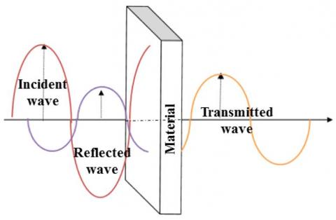
The interactions between electromagnetic waves and materials can be divided into three mechanisms: reflection, absorption and multiple reflections within the shield. The first mechanism, reflection, depends on the permittivity and conductivity of the material. The reflection increases proportionally, at the same time, with the permittivity and the conductivity of the material. The second mechanism of protection against electromagnetic interference is absorption, which requires the existence of mobile charge carriers (electrons or holes), which interact with electromagnetic radiation. The third mechanism of attenuation of electromagnetic interference is the multiple reflections; this mechanism depends on the physical properties and the geometric shape effect of the shielding material. When the material is thicker, this third mechanism can be neglected [4-6].
Electromagnetic shielding is the main effective solution to reduce interference and interactions between devices or subcomponents of the devices themselves [6-7]. In general, materials of good electrical conductivity such as copper, aluminum, etc. have good shielding performance. Copper is one of the most widely used metals in this field and is extremely versatile and advantageous for a wide variety of applications because of its mechanical and electrical properties. Copper is a malleable and ductile material. In addition, copper and copper alloy pieces show a highly ductile behavior [8-11].
The plastic deformation of a material can be defined as a permanent deformation or change in shape of a solid boby without fracture. This occurs when a sufficient stretching force is applied to a material leading to a significant elongation. In this case, two distinguishable deformations can be observed first an elastic deformation followed by a plastic deformation. The elastic deformation is reversible when the stress is released before the elastic limit, therefore the material returns to its original shape. For the plastic deformation even after the release of the stretching force a permanent deformation of the material remains [12-14].
The study of plastic deformation is probably due to the need of controlling the shaping and use of materials. As a result, this has long been empirical and it is only in recent decades that the concepts necessary to understand the physical phenomena that occur during plastic flows have been developed [15-17]. For crystalline solids, the basic mechanisms are fairly well known, but the effect of plastic deformation on shielding efficiency (electrical parameters) is poorly known and is currently a promising area of research [18-20].
Several researchers [13, 15-16] obtained preliminary results, studying the effect of the interaction of dislocations that interact during plastic deformation on electrical properties. In the present work, we study the effect of plastic deformation on shielding immunity of copper against electromagnetic interference (EMI).
The aim of this work is to perform a preliminary analysis of the variation of the electrical property (electrical conductivity) according to the internal stresses generated by the plastic deformation of a high purity metallic copper (99%), hence making possible to see the shielding efficiency of Cu as function of the mechanical deformation rate (plastic domain) in the frequency range [0-1 GHz].
The rapid increase in electromagnetic applications has also increased the need for EMI protection materials. The attenuation of electromagnetic radiation is one of the main indicators for measuring the effectiveness of EMI shielding. This indicator is the ratio of the intensity of an electromagnetic signal before and after the shield. In other words, the propagation of electromagnetic waves from one region to another can be efficiently controlled by electromagnetic wave insulating materials. These materials are selected according to the desired applications [21]. The efficiency of the shielding (SE) is a property of the materials indicating the ability to fight against undesirable electromagnetic interference [1, 3, 7].
In this work, the parameter S obtained from the vector network analyzer was used to calculate the total EM EMI as follows:
$\mathrm{SE}=10 \log \frac{1}{\left|\mathrm{S}_{12}\right|^{2}}=10 \log \frac{1}{\left|S_{21}\right|^{2}}$ (1)
where Sij represents the power transmitted from port i to port j.
Also, the shielding effectiveness (SE, dB) of the shielding material (show Figure 2) can be expressed as [4, 6]:
$S E=S E_{R}+S E_{A}+S E_{B}$ (2)
where SEA and SER are the absorption and reflection loss respectively; SEB is the multiple reflection loss. They can be further expressed as:
$S E_{R}=20 \log \left(Z_{0} / 4 Z_{s}\right)$ (3)
$S E_{A}=20 \log \left(e^{-2 d / \delta}\right)$ (4)
$S E_{B}=20 \log \left(1-e^{-2 d / \delta}\right)$ (5)
$\delta=(f \pi \sigma \mu)^{1 / 2}$ (6)
where f is the frequency (Hz) of electromagnetic waves, σ is the electrical conductivity, μ is the magnetic permeability, d is the thickness (mm) of the shielding materials, Z0 is the intrinsic impedance of an electric wave ZS is impedance of shield and $\delta$ means the skin depth.
Figure 1. Different mechanism of shielding
When a load is applied to a metallic material, enough to provoke deformation, this material deforms by changing its sizes. This is the result of a reversible elastic deformation followed by an irreversible plastic one even after unloading. The plastic deformation at a macroscopic scale of crystalline material finds explanation at a microscopic scale by generation and mobility of multiple dislocation lines known in mechanics as internal stresses. Plastic deformation occurs when loading is enough to deform definitively a material. In other words, plastic deformation is a permanent deformation or a change in shape without breaking under the effect of stress. Plastic deformation provokes dislocations inside materials making them thermodynamically unbalanced [22-23].
$\sigma=E \cdot \varepsilon$ (7)
where σ is the stress, E the Young's modulus and $\mathcal{E}$ the deformation
Figure 2. Material deformation curve
4.1 Samples preparation
The sizes of the copper sample for the tensile test as a total size of 150 × 70 × 4 mm³. The effective size of the sample in which the TEM test is performed is 70 × 70 mm2 with a thickness of 1 mm (Figure 3). To meet this size requirement, the samples intended for carrying out the plastic deformation by tensile test required the making of test pieces from larger copper sheets according to the following steps:
The test pieces were cut from larger copper sheets with a thickness of 4 mm. The sample got had a size of 150X70X4 mm³ also to reach the shielding measurement requirements, the thickness of central area of the sample (i.e. 70 × 70 mm2) was milled with a very small step of 0,05 mm with a rotational speed of 500 rpm until to reach a thickness of 1 mm.
To achieve a shine surface aspect a delicate polishing is performed with fine-grained abrasive paper, it also allowed eliminating surface microcraks generated by the milling operation.
Figure 3. Deformation of Cu by unidirectional traction
4.2 Plastic deformation
With the aim of achieving a more or less homogeneous plastic deformation in the useful zones of the specimens and taking into account the copper ductility, a deformation rate of 10 μm/s was imposed, avoiding microcracks formation and introducing dislocations (internal stresses). The deformation was performed with a rate of 3 % for the 1st samples group to 2% for the 2nd and without deformation for the 3rd. Note, that our tensile test specimens were deformed until necking so that the deformation was obtained in the zone of the homogeneous plastic field; this plastic deformation homogeneity is requisite for satisfactory measurement of the shielding effectiveness in the double TEM cell (DTEM)
The samples are deformed at 2 % and 3 % and other samples without plastic deformation in order to compare their shielding efficiency as a function of the deformation rates.
Cells of measurement the shielding efficiency
4.3 Definition of TEM cell
The TEM cell is a closed chamber; it has the principle of a tri-plate transmission line. The TEM cell consists of two ground planes, interposed by a central conductor, which is usually referred by the English term "septum". In the TEM cell, the electromagnetic wave propagates and passes through the sample (TEM mode) providing that the wavelength is less than the transverse dimension of the cell [24].The use of the TEM cell is limited by the cutoff frequency of this mode. The latter is fixed by the dimensions of the cell which are chosen so as to allow only the generation of a TEM mode.
4.4 DTEM cell
The DTEM cell (dual TEM cell) is composed of two TEM cells that coupled through an opening in a common wall (Figure 18), one of these cells is used for the emission of the electromagnetic field and the other for the reception. The theory of the small aperture is often used to explain, the coupling between the two cells [24]. In general, the coupling opening takes a circular or squared shape.
Figure 4. Dual cell TEM
When the transmitting cell is excited, part of the electromagnetic field is transmitted to the receiver cell through the opening. The transmitted field results in the appearance of voltages at the connectors of the receiving cell.
When an element under test is put on the opening, the coupling of the two cells is reduced. This reduction gives a direct measurement of the shielding efficiency.
The DTEM cell allows the separation between the electric field and magnetic field, this is explained by the theory of the small opening [25-26]. If the opening is electrically small, then the diffusion effect is substantially equivalent to that produced by the set. This dipole moment can be used to predict scattered fields, which in the case of the double TEM cell gives a description of the opening coupling. The dipole moments depend on the incidences of the fields and the shape of the opening (opening polarizability).
5.1 X-ray diffraction results
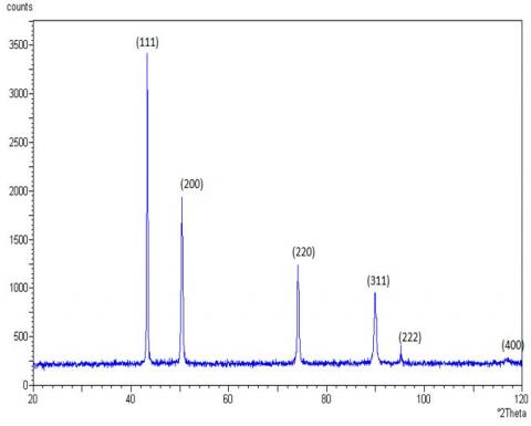
In this part of the work, was proceeded the X-ray diffraction analysis of the Cu samples. These samples are tested under X-rays before and after the plastic deformation. This operation aims to control the state of the microstructure of our material.
The analysis of these diffractograms shows the superposability of the reflection peaks of the same reflector planes families, thus proving that Cu samples did not undergo any phase change following a plastic deformation imposed to Cu, but also without any change of the microstructure. Moreover, according to the theory of dislocation mobility, the samples, after plastic deformation, underwent an introduction of dislocations.
Figure 5. Xray results of Cu before stress
Figure 6. XRD diffractograms of Cu samples after deformation
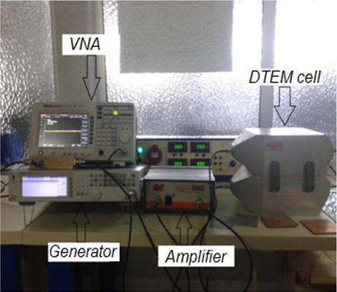
Figure 7 shows the measurement set up for the shielding effectiveness of the samples which consists of a vectorial network analyzer (VNA), an amplifier, a frequency generator, and a DTEM cell. This measures the direct and reflected signal amplitude as a function of the frequency.
Figure 7. The shielding efficiency measuring device
5.2 Shielding effectiveness results
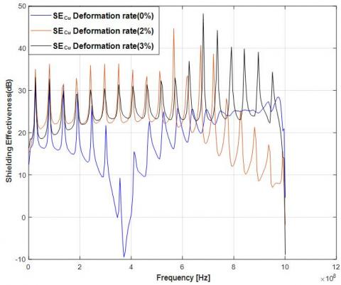
Figure 8 presents the results of shielding effectiveness against the electric field of the three Cu prepared samples with a high purity of 99 %. These results are obtained thanks to the DTEM chamber used in the frequency range 0-1 GHz. The results obtained on the first Cu sample (undeformed) exhibits a single peak at 380 MHz. The SE of the second sample with 2 % deformation is higher than the first (undeformed) for frequencies under 600 MHz and the peak of resonance is delayed up to 1 GHz. This is due to the dislocations generated by the mechanical traction of the Cu sample. For the third sample with 3 % deformation, it exhibited a good SE compared to the two firsts samples for the frequency range used for this study. This better performance can be explained by a higher increase in the dislocation density. It is well known that dislocations occur at the angstrom scale and are generated by the linear stretching of the metal, affecting as such positively the SE behavior of Cu, as it has been demonstrated in this article. It can be concluded that dislocations play a key role in trapping the electric waves inside the materials reducing thereby outside reflections. These promising results open new perspectives for shielding applications for the development of new equipment subjected to electromagnetic fields and therefore avoiding equipment failure.
Figure 8. Comparison of the experimental shielding effectiveness results of Cu samples with 0, 2 and 3 % deformation respectively
This work deals with the effects of plastic deformation on the shielding electromagnetic efficiency SE of copper. The use of DTEM for the SE measurement has allowed seeing a proportional evolution of SE as a function of the plastic deformation rate. It was found that the higher the deformation rate the higher the dislocation density. The dislocation advantageously traps a maximum of electric and/or electromagnetic waves and dissipates their energy inside the material instead of dissipating them outside it. This makes possible to increase the electromagnetic shielding efficiency of copper. Such behavior is very similar to the role played by carbon fiber in composite material. According to equation (5) and (6), this efficiency varies also proportionally to the electrical copper conductivity. This allows us to conclude that this latter is also proportional to the plastic strain rate applied to the material. Consequently, these experimental results got in this article have proved that the copper electromagnetic shielding quality can be improved by controlled plastic deformation, and can be regarded as noticeable progress.
This work was supported partly by the Polytechnic Military School of Bordj El Bahri of Algiers. The authors would like to thank, for his assistance, for his valuable advice and to have provided the material and equipment, Pr.Chabira Fouad Salem of the mechanical laboratory (lme), at the mechanic's department of Laghouat University.
[1] Danlée, Y., Bailly, C., Huynen, I. (2014). Thin and flexible multilayer polymer composite structures for effective control of microwave electromagnetic absorption. Composites Science and Technology, 100: 182-188. https://doi.org/10.1016/j.compscitech.2014.06.010
[2] Gaoui, B., Hadjadj, A., Kious, M. (2017). Enhancement of the shielding effectiveness of multilayer materials by gradient thickness in the stacked layers. Journal of Materials Science: Materials in Electronics, 28(15): 11 292-11 299. https://doi.org/10.1007/s10854-017-6920-8
[3] Danlée, Y., Huynen, I., Bailly, C. (2012). Thin smart multilayer microwave absorber based on hybrid structure of polymer and carbon nanotubes. Applied Physics Letters, 100(21): 213105. https://doi.org/10.1063/1.4717993
[4] Thomassin, J.-M., Vuluga, D., Alexandre, M., J´erôme, C., Molenberg, I., Huynen, I., Detrembleur, C. (2012). A convenient route for the dispersion of carbon nanotubes in polymers: Application to the preparation of electromagnetic interference (emi) absorbers. Polymer, 53(1): 169-174. https://doi.org/10.1016/j.polymer.2011.11.026
[5] Tahar, M., Hadjadj, A., Kious, M., Arun Prakash, V.A., Gaoui, B. (2018). Effect of magnetic iron (iii) oxide particle addition with mwcnts in kenaf fibre-reinforced epoxy composite shielding material in ‘e’,‘f’,‘i’ and ‘j’ band microwave frequencies. Materials Research Express, 6(4). https://doi.org/10.1088/2053-1591/aaf9de
[6] Gaoui, B., Hadjadj, A., Kious, M. (2016). Comparison electromagnetic shielding effectiveness between single layer and multilayer shields. in Power Engineering Conference (UPEC), 2016 51st International Universities. IEEE, pp. 1-5. https://doi.org/10.1109/UPEC.2016.8114106
[7] Gaoui, B., Hadjadj, A., Kious, M. (2017). Novel multilayer arrangement of conductive layers traps the electromagnetic interferences by multiple internal reflections at high frequency in the far field. Journal of Materials Science: Materials in Electronics, 28(4): 3924-3930. https://doi.org/10.1007/s10854-016-6006-z
[8] He, Y., Ao, J., Yang, J., Tang, X. (2014). The shielding-effectiveness based magnetic field shielding theory and its application in mobile payment systems. in Vehicular Technology Conference (VTC Fall), 2014 IEEE 80th. IEEE, pp. 1-5. https://doi.org/10.1109/VTCFall.2014.6966203
[9] Lou, C.-W., Lin, T.A., Chen, A.-P., Lin, J.-H. (2016). Stainless steel/polyester woven fabrics and copper/polyester woven fabrics: Manufacturing techniques and electromagnetic shielding effectiveness. Journal of Industrial Textiles, 46(1): 214-236. https://doi.org/10.1177/1528083715580518
[10] Tong, X.C. (2016). Advanced materials and design for electromagnetic interference shielding. CRC press.
[11] Papanikolaou, S., Cui, Y., Ghoniem, N. (2017). Avalanches and plastic flow in crystal plasticity: An overview. Modelling and Simulation in Materials Science and Engineering, 26(1): 013001. https://doi.org/10.1088/1361-651X/aa97ad
[12] Borodin, E.N., Mayer, A.E. (2015). Structural model of mechanical twinning and its application for modeling of the severe plastic deformation of copper rods in Taylor impact tests. International Journal of Plasticity, 74: 141-157. https://doi.org/10.1016/j.ijplas.2015.06.006
[13] Hubert, O., Lazreg, S. (2012). Multidomain modeling of the influence of plastic deformation on the magnetic behavior. IEEE Transactions on Magnetics, 48(4): 1277-1280. https://doi.org/10.1109/TMAG.2011.2172935
[14] Li, J., Li, F., Zhao, C., Chen, H., Ma, X., Li, J. (2016). Experimental study on pure copper subjected to different severe plastic deformation modes. Materials Science and Engineering: A, 656: 142-150. https://doi.org/10.1016/j.msea.2016.01.018
[15] Rodrigues-Jr, D., Silveira, J., Gerhardt, G., Missell, F., Landgraf, F., Machado, R., de Campos, M. (2012). Effect of plastic deformation on the excess loss of electrical steel. IEEE Transactions on Magnetics, 48(4): 1425-1428. https://doi.org/10.1109/TMAG.2011.2174214
[16] Lazreg, S., Hubert, O. (2012). Influence of plasticity on magnetic and magnetostrictive behaviors of dual-phase steel. IEEE Transactions on Magnetics, 48(4): 1273-1276. https://doi.org/10.1109/TMAG.2011.2172936
[17] Daniel, L. (2018). An analytical model for the magnetostriction strain of ferromagnetic materials subjected to multiaxial stress. The European Physical Journal Applied Physics, 83(3): 30904. https://doi.org/10.1109/TMAG.2013.2239264
[18] Daniel L., Hubert, O., Buiron, N., Billardon, R. (2008). Reversible magneto-elastic behavior: A multiscale approach. Journal of the Mechanics and Physics of Solids, 56(3): 1018-1042. https://doi.org/10.1016/j.jmps.2007.06.003
[19] Hahner, P., Bay, K., Zaiser, M. (1998). Fractal dislocation patterning during plastic deformation. Physical Review Letters, 81(12): 2470-2473. https://doi.org/10.1103/PhysRevLett.81.2470
[20] Jakobsen, B., Poulsen, H.F., Lienert, U., Almer, J., Shastri, S.D., Sørensen, H.O., Gundlach, C., Pantleon, W. (2006). Formation and subdivision of deformation structures during plastic deformation. Science, 312(5775): 889-892. https://doi.org/10.1126/science.1124141
[21] Saini, P., Arora, M. (2012). Microwave absorption and emi shielding behavior of nanocomposites based on intrinsically conducting polymers, graphene and carbon nanotubes. in New Polymers for Special Applications. InTech. https://doi.org/10.5772/48779
[22] Dewers, T.A., Issen, K.A., Holcomb, D.J., Olsson, W.A., Ingraham, M.D. (2017). Strain localization and elastic-plastic coupling during deformation of porous sandstone. International Journal of Rock Mechanics and Mining Sciences, 98: 167-180. https://doi.org/10.1016/j.ijrmms.2017.06.005
[23] Gupta, Y., Mandal, A. (2017). Elastic-plastic deformation of molybdenum single crystals shocked to 12.5 gpa: Crystal anisotropy effects. in APS Shock Compression of Condensed Matter Meeting Abstracts. https://doi.org/10.1063/1.5048131
[24] Voicu, V., P˘atru, I., Nicolae, P.M., Dina, L.A. (2017). Analyzing the attenuation of electromagnetic shielding materials for frequencies under 1 ghz. in Advanced Topics in Electrical Engineering (ATEE), 2017 10th International Symposium on. IEEE, 2017, pp. 336-339. https://doi.org/10.1109/ATEE.2017.7905057
[25] Pan, S.M., Kim, J., Kim, S., Park, J., Oh, H., Fan, J. (2010). An equivalent three-dipole model for IC radiated emissions based on TEM cell measurements. In: 2010 IEEE International Symposium on Electromagnetic Compatibility. IEEE, pp. 652-656. https://doi.org/10.1109/isemc.2010.5711354
[26] Tumayan, R., Bunlon, X., Reineix, A., Andrieu, G., Guiffaut, C. (2014). A method using an open TEM cell to extract the complex permittivity of an unknown material. 2014 International Symposium on Electromagnetic Compatibility. IEEE. https://doi.org/10.1109/emceurope.2014.6931067